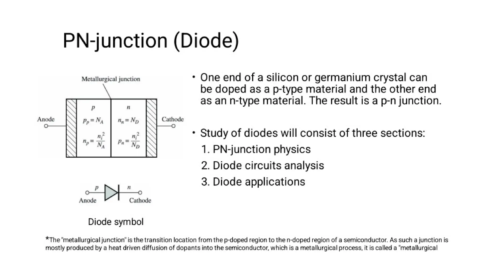
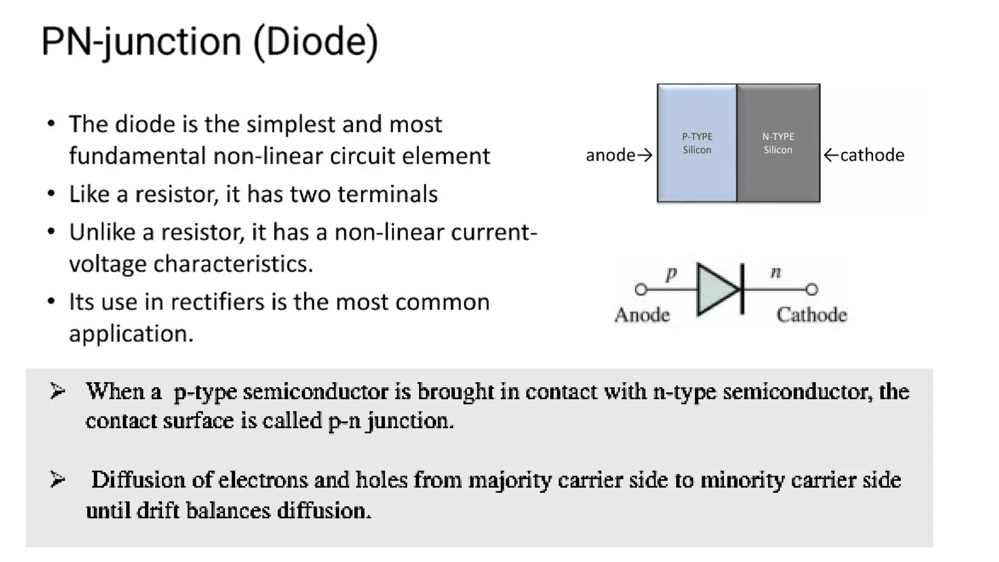
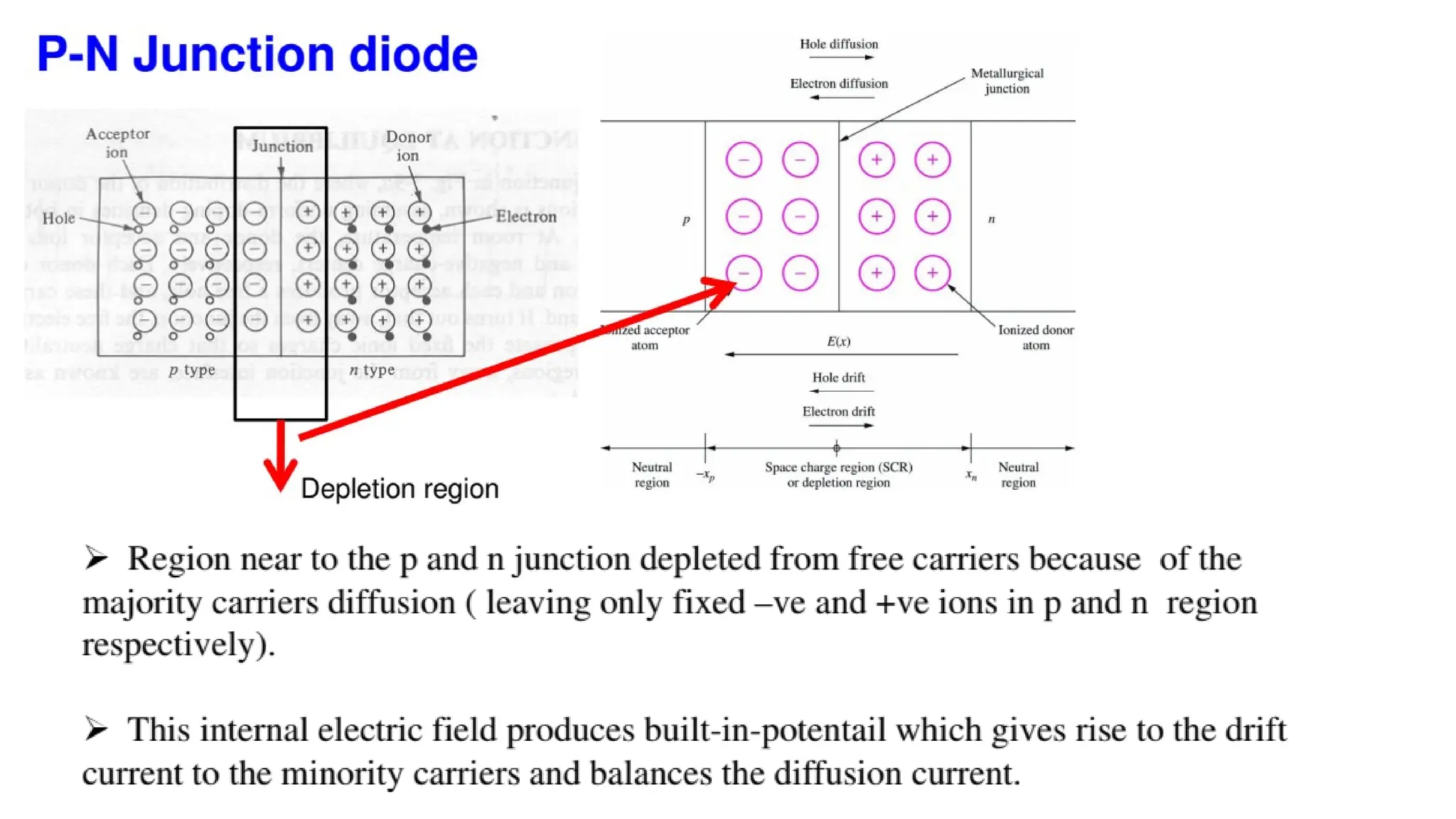
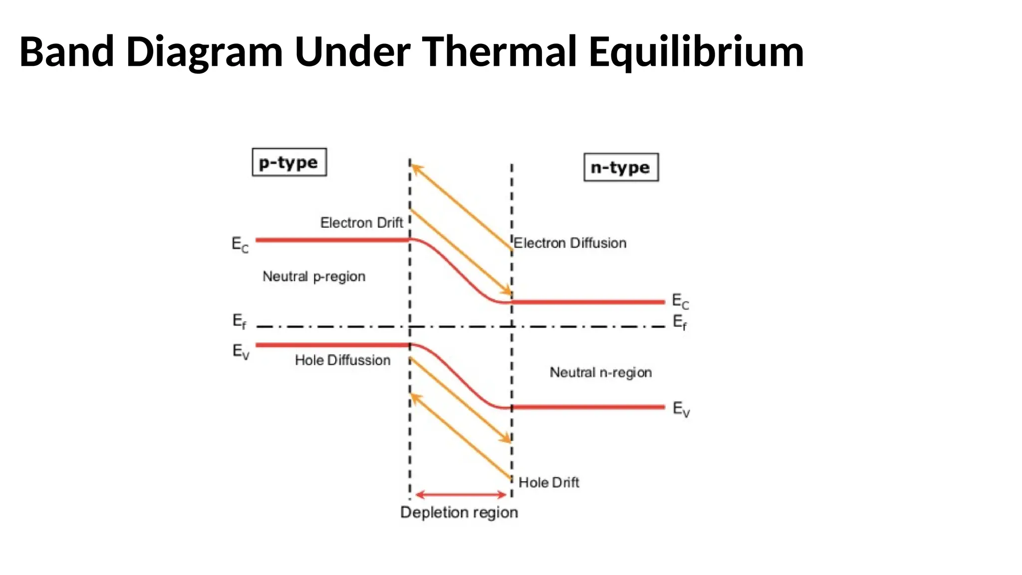
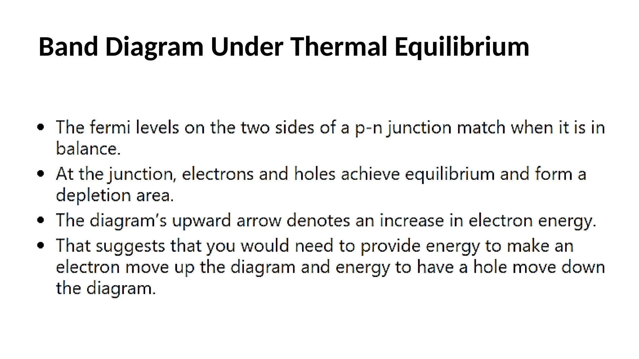
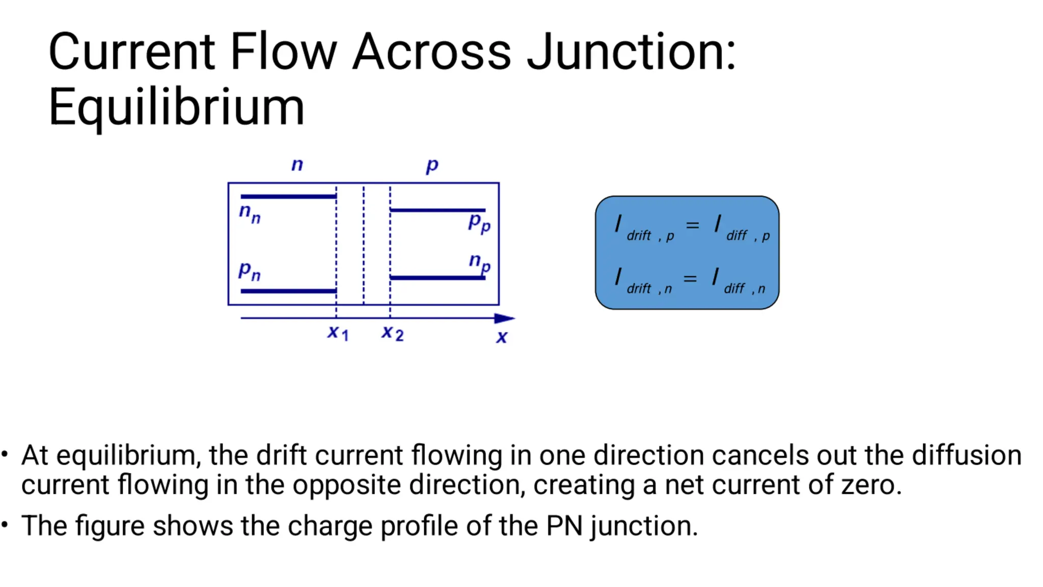
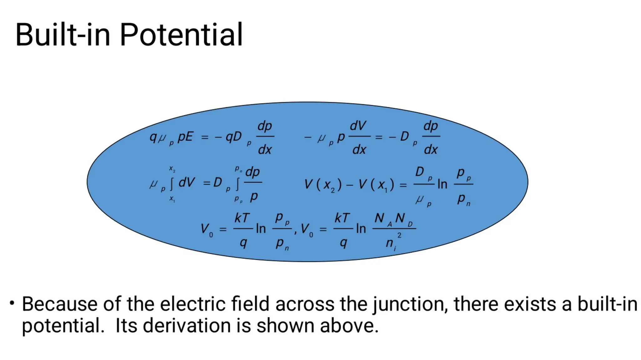
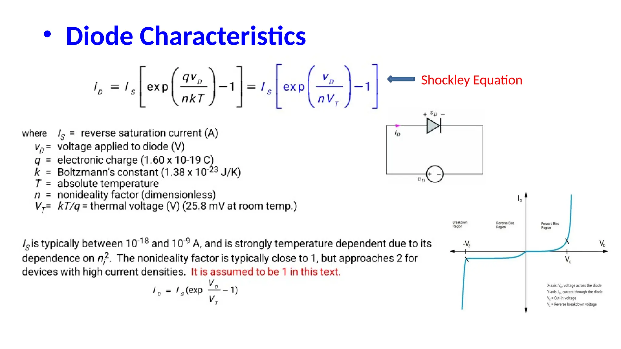
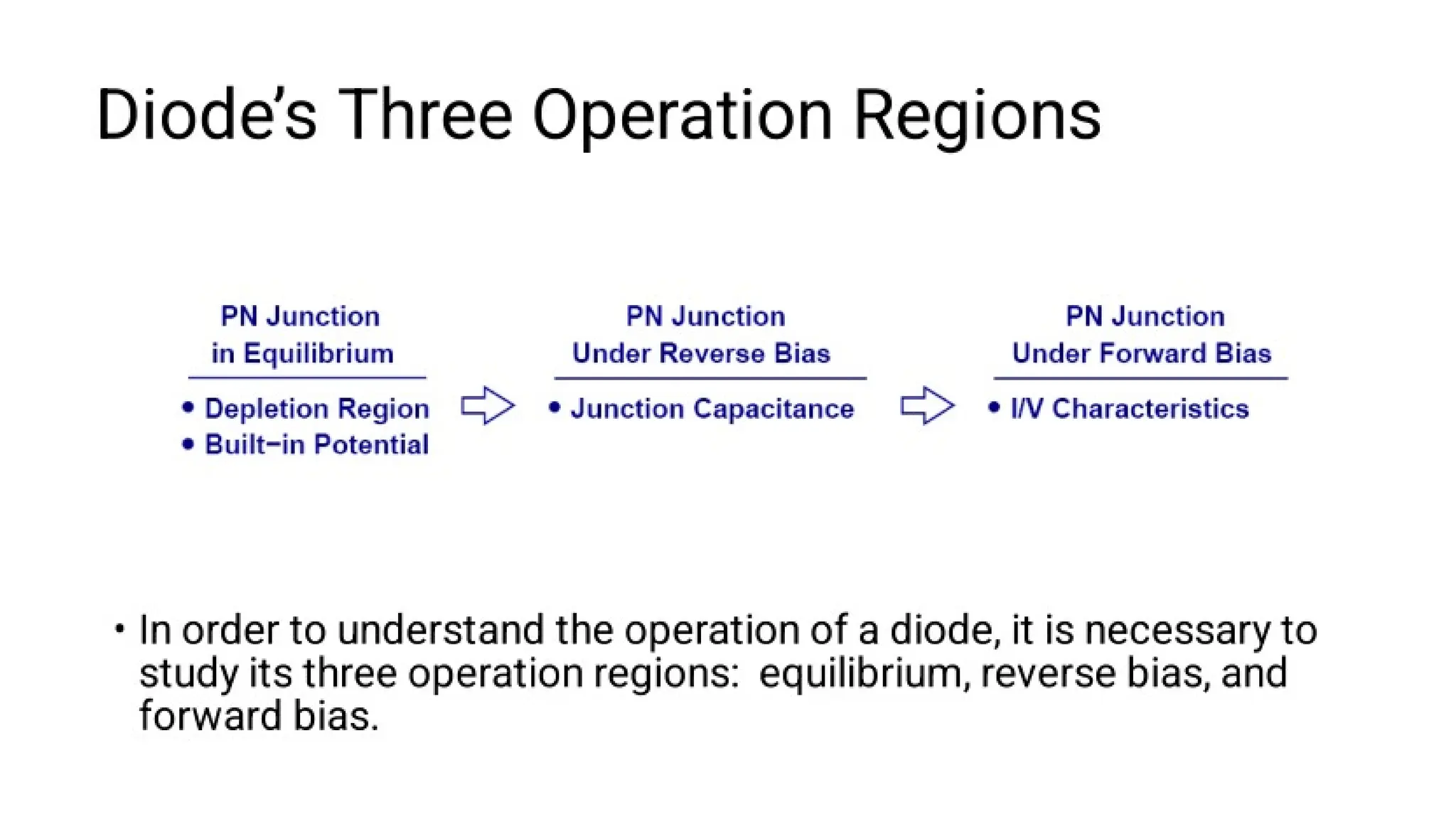
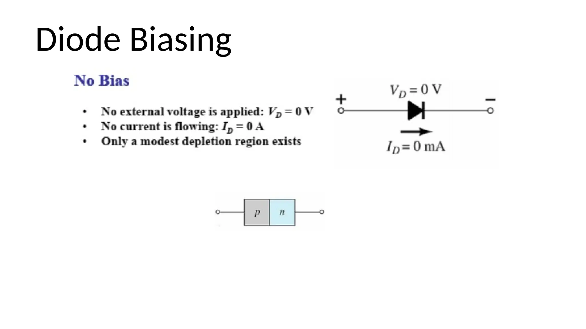
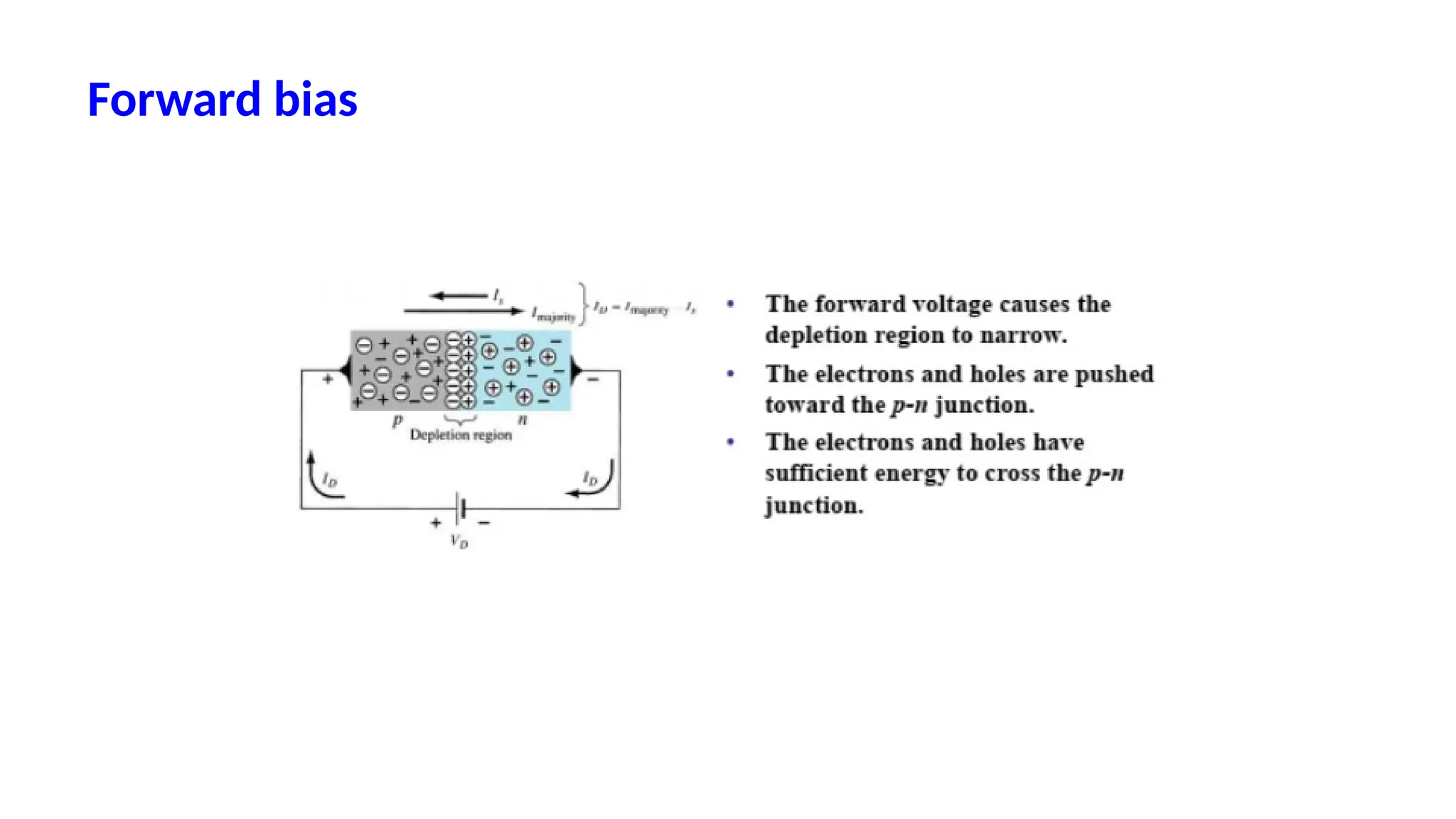
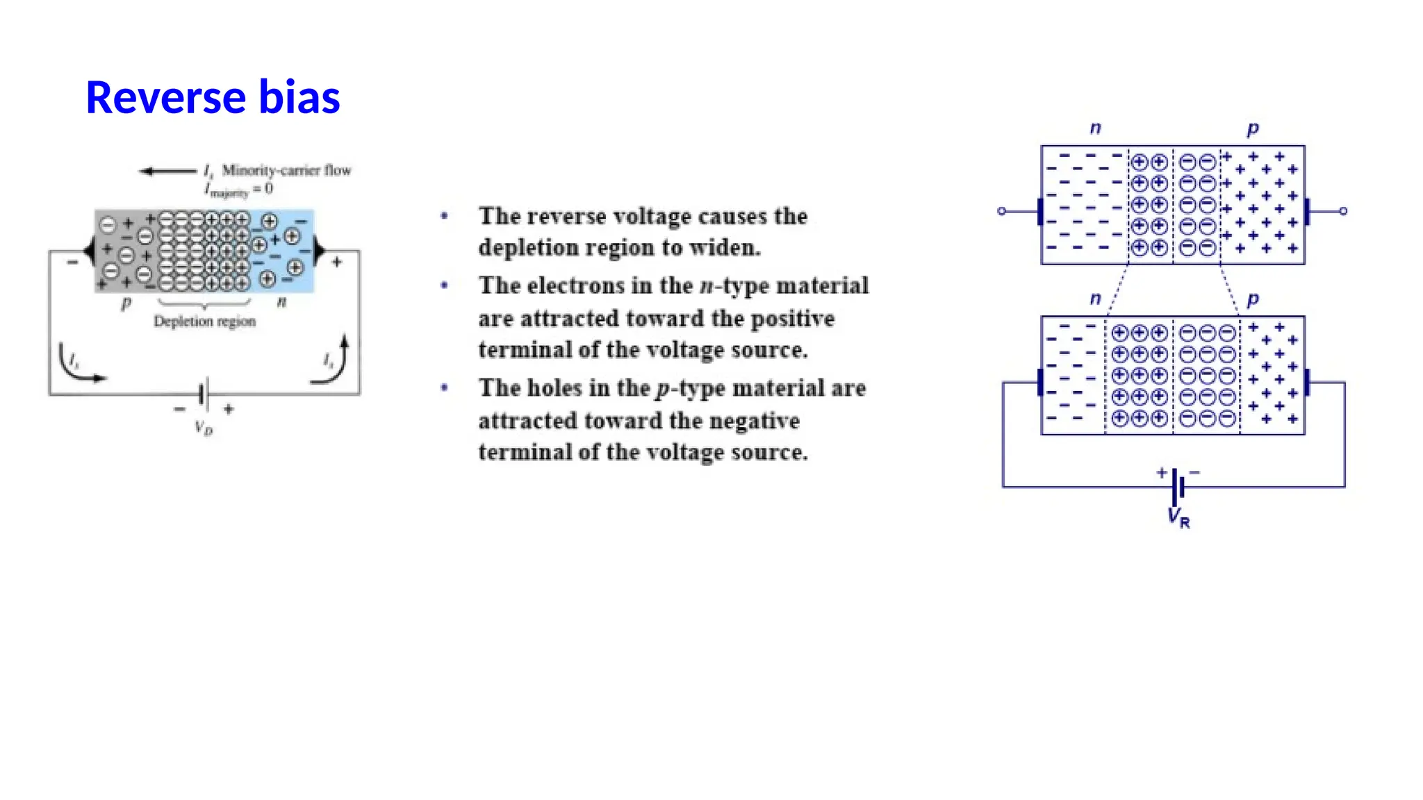
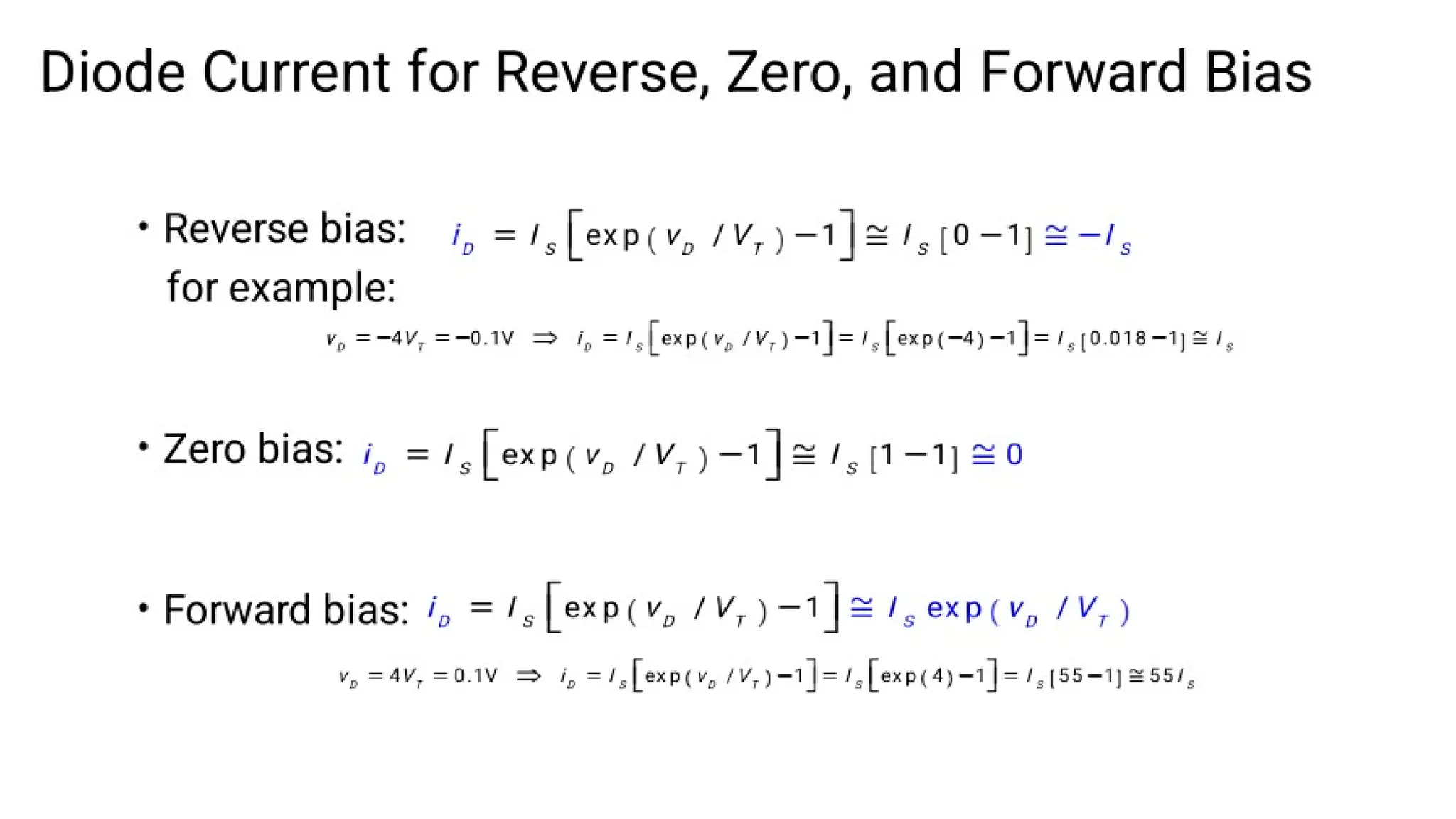
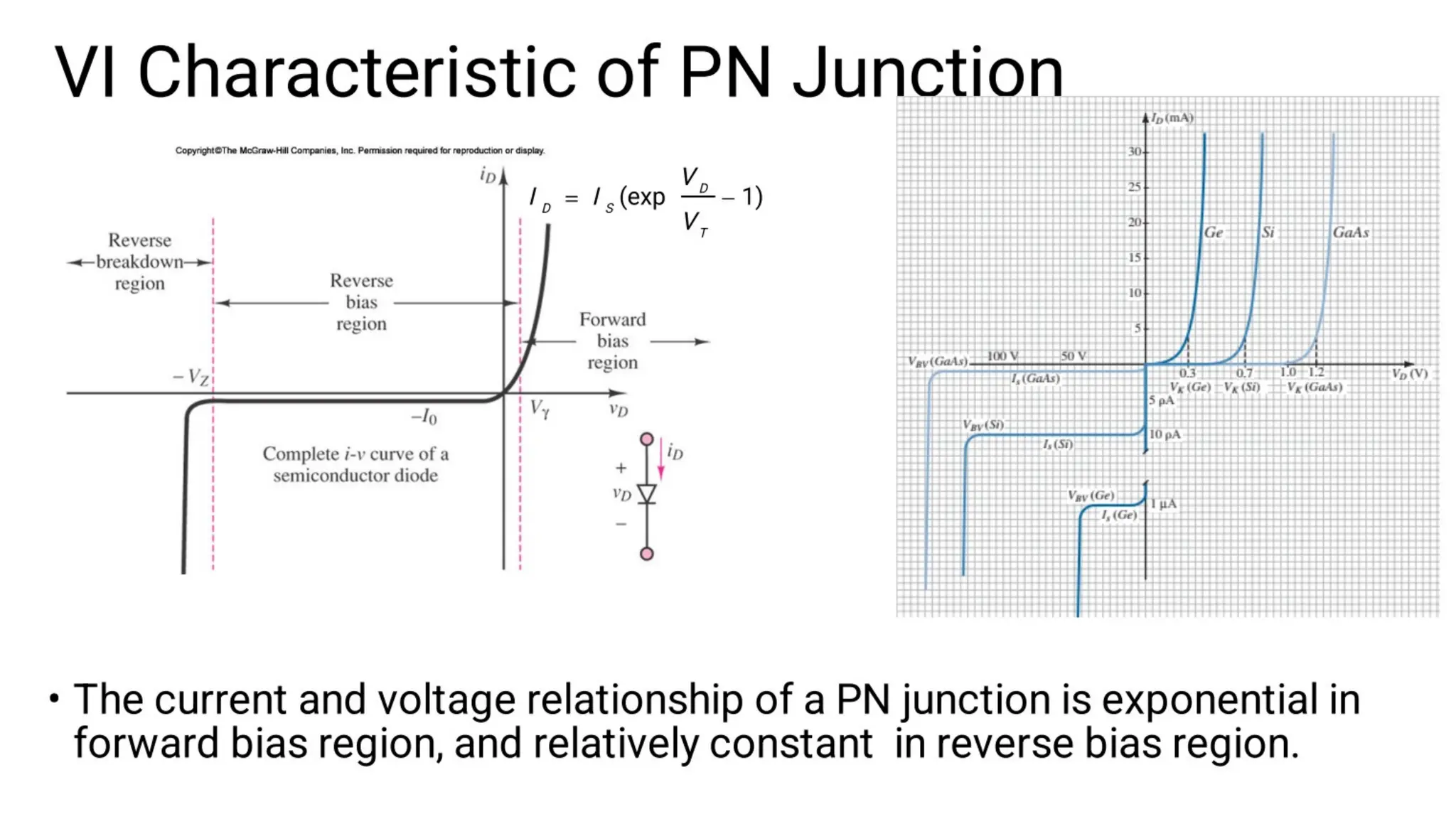
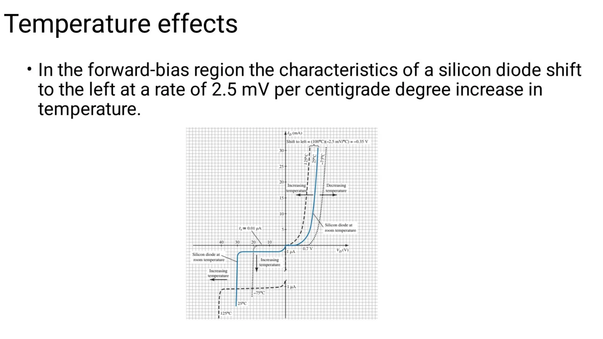
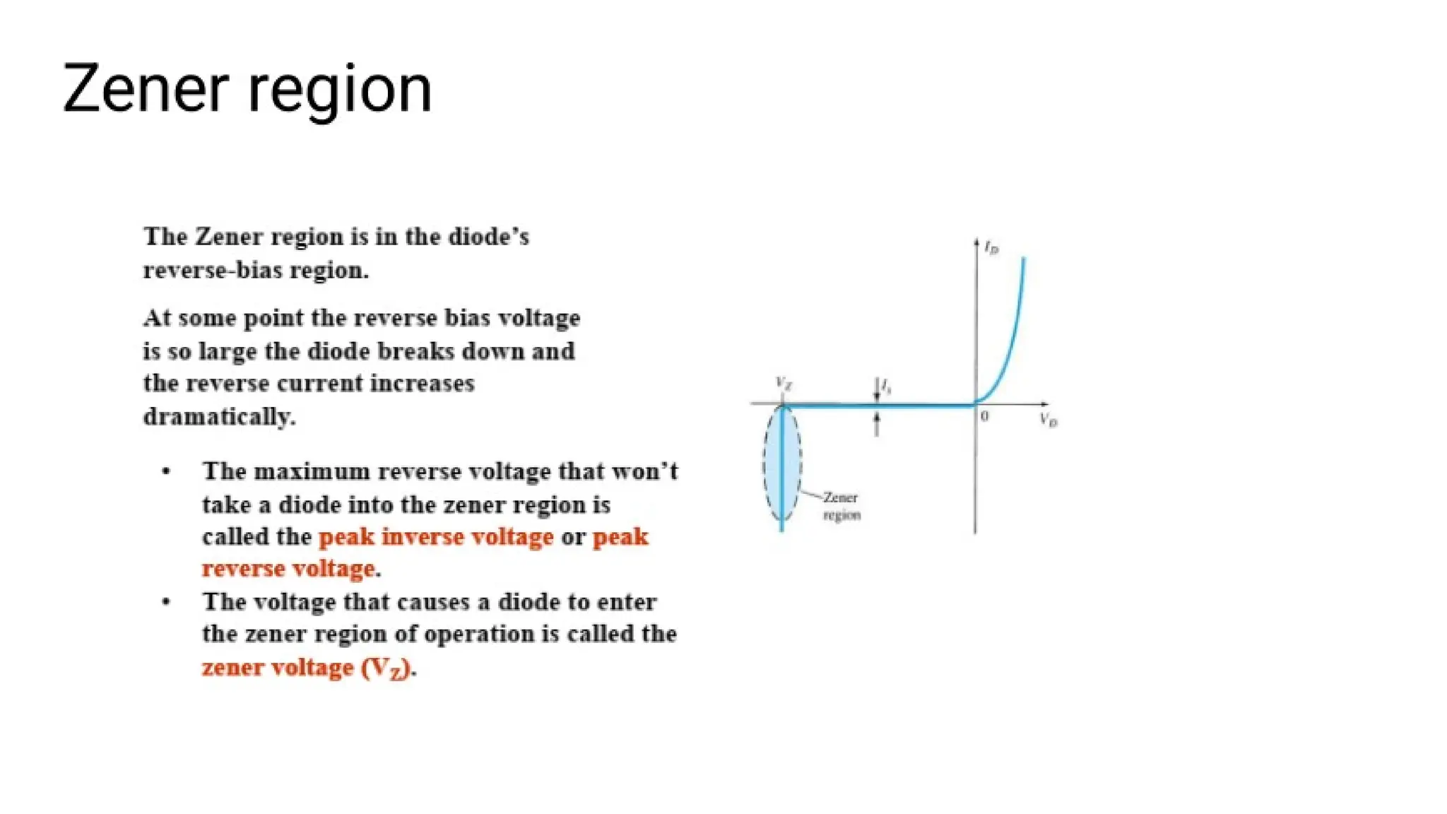
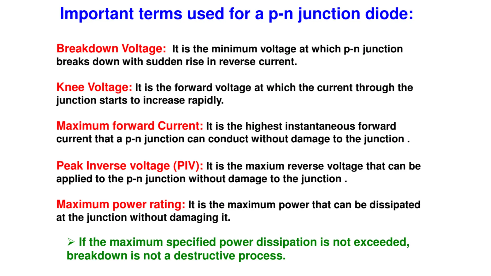
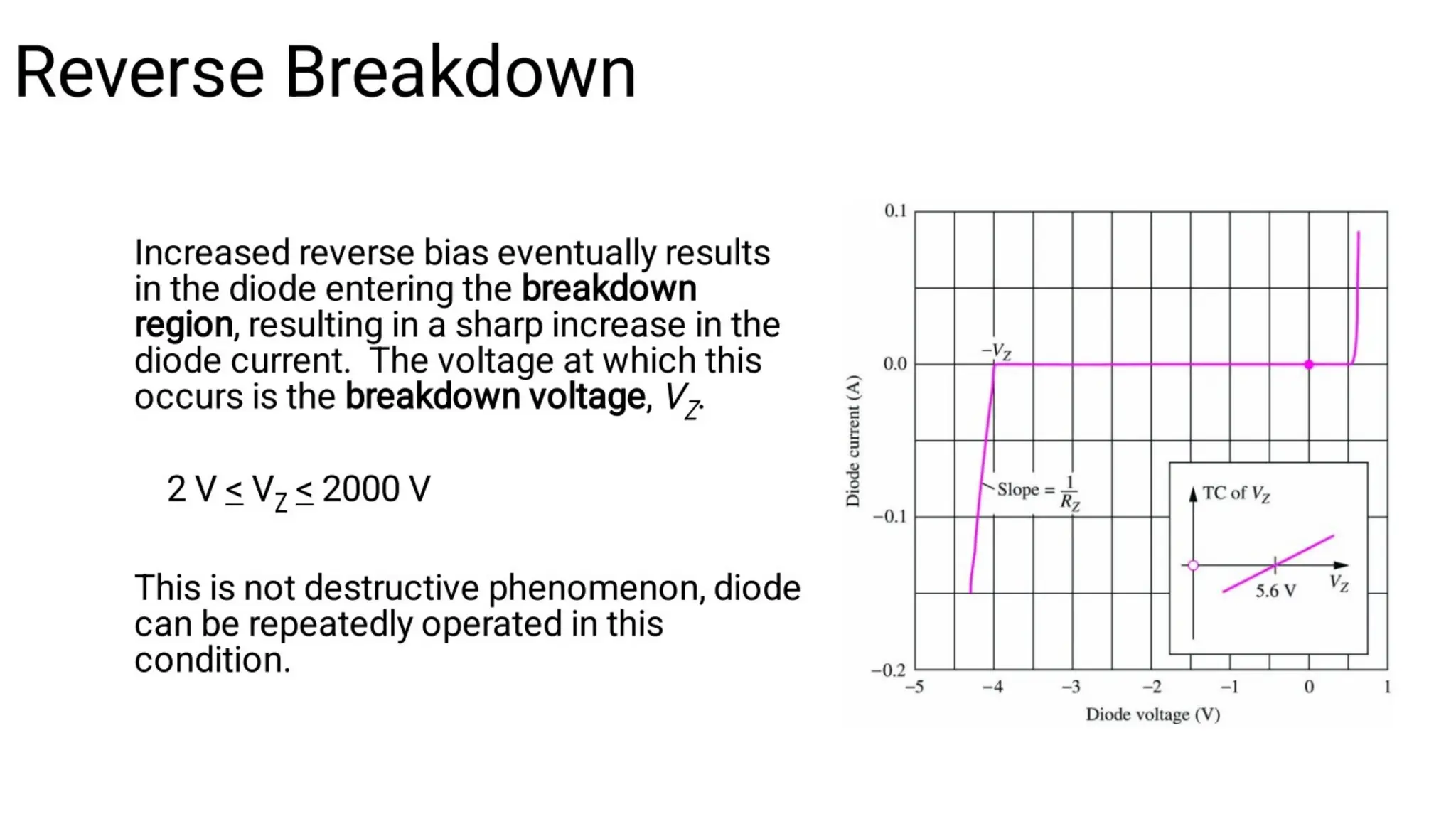
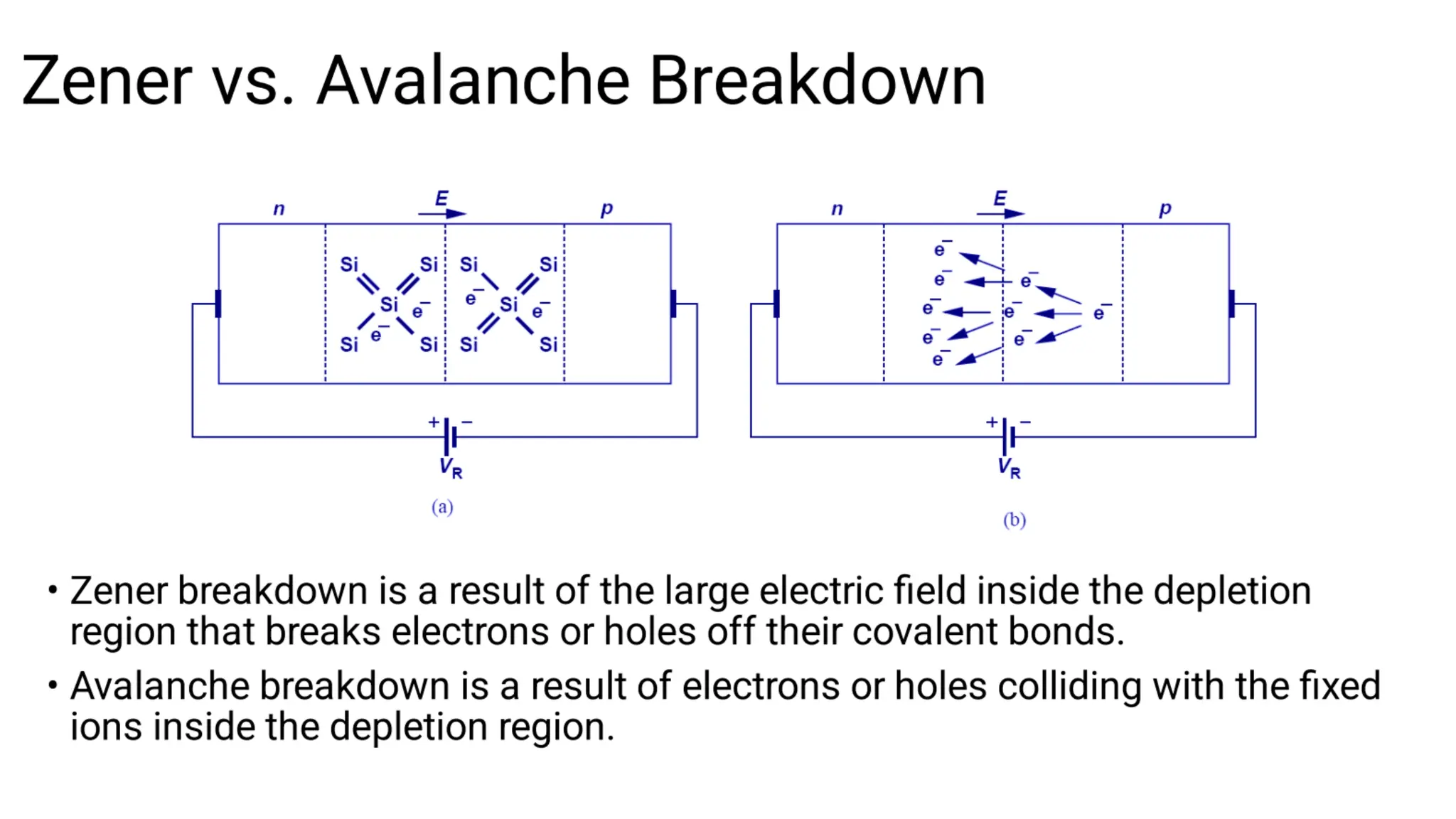
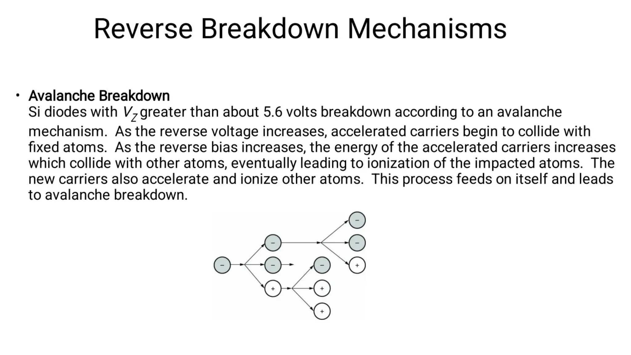
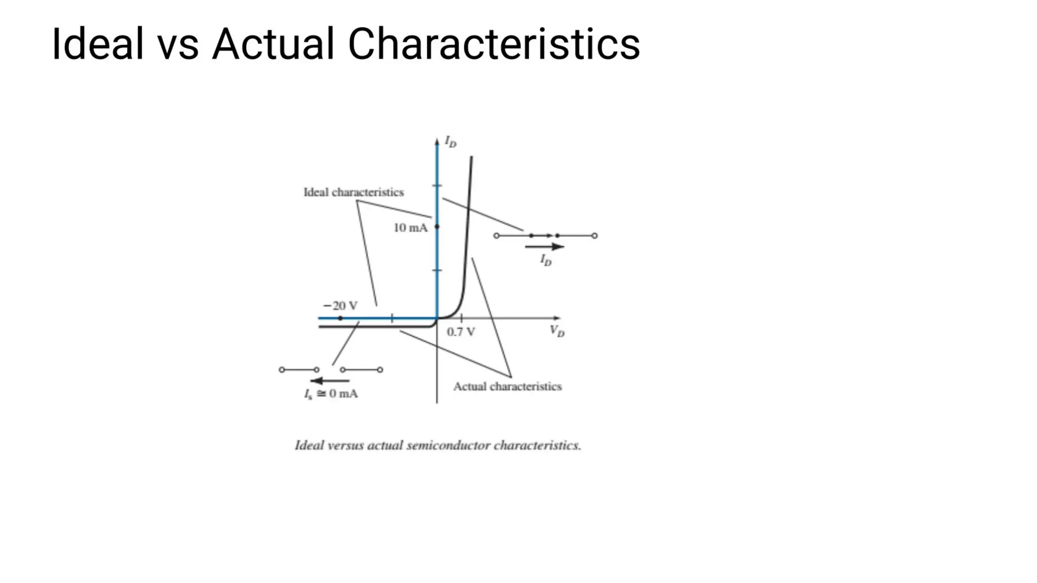
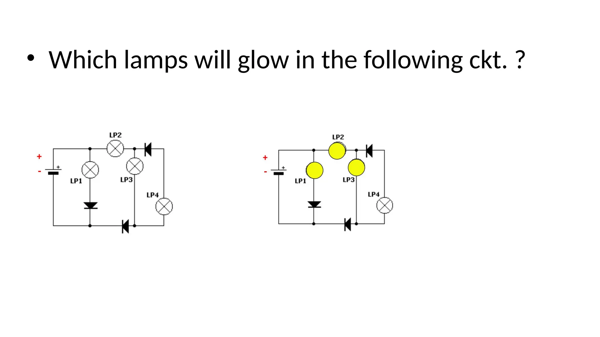
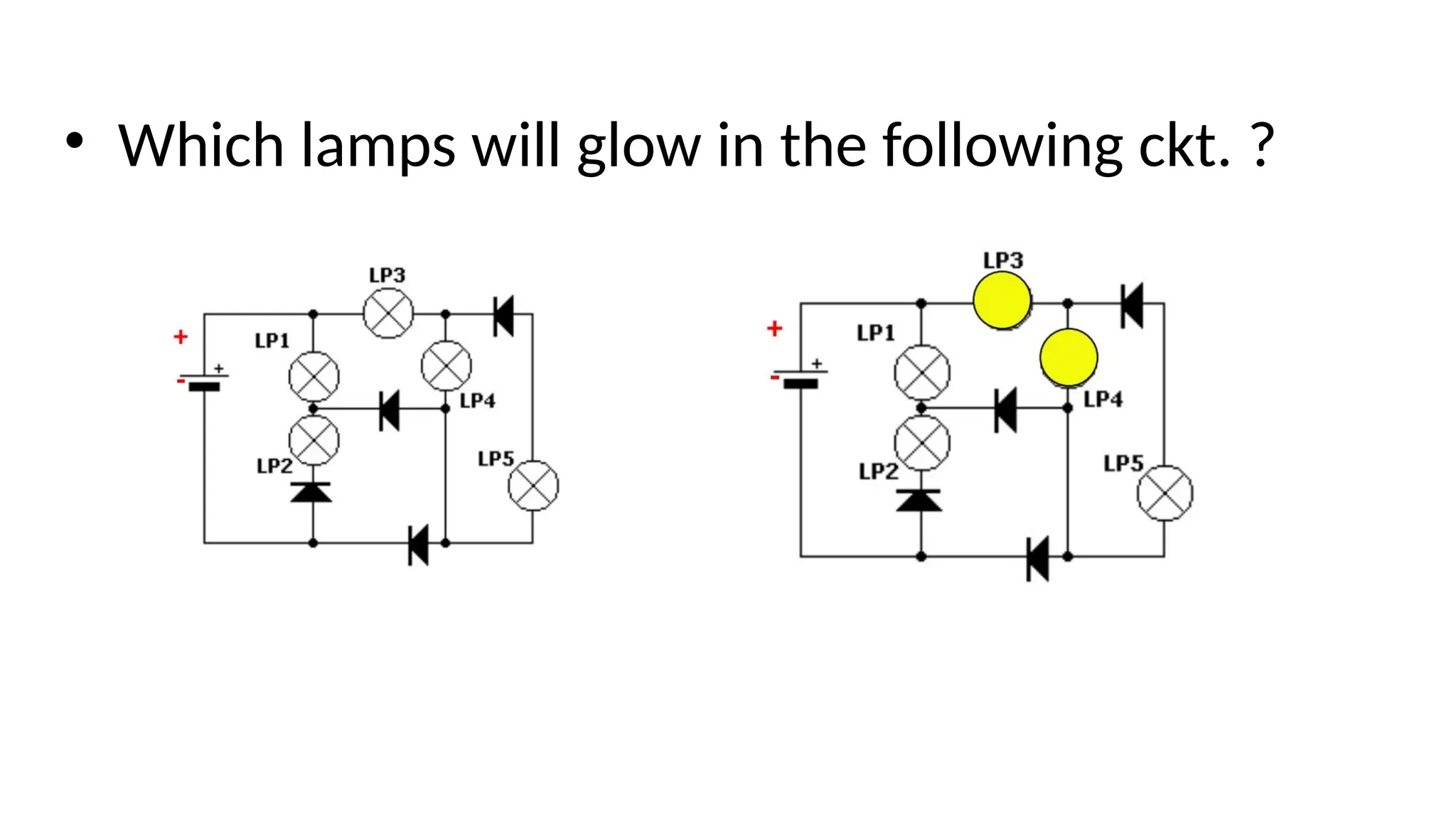
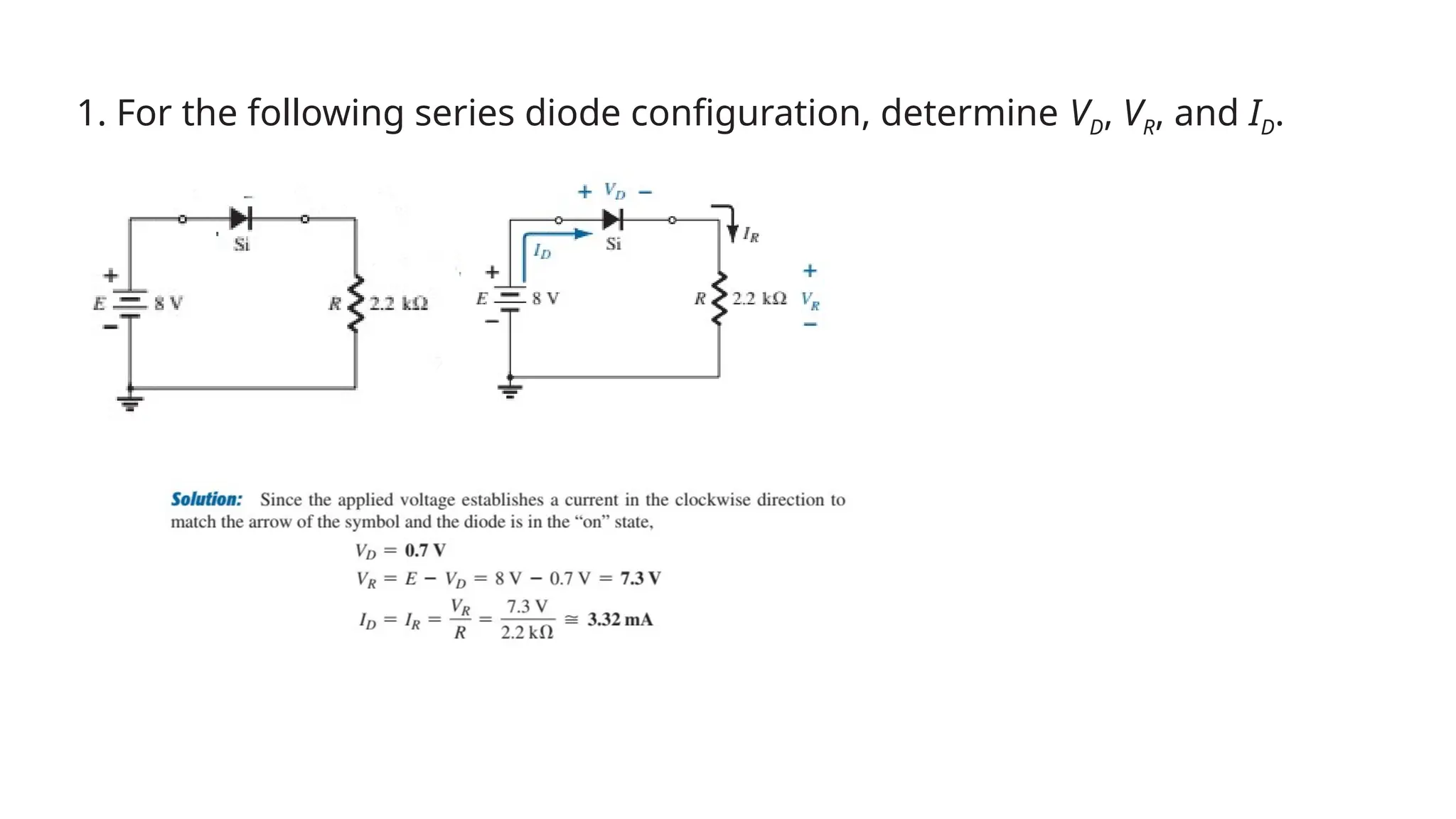
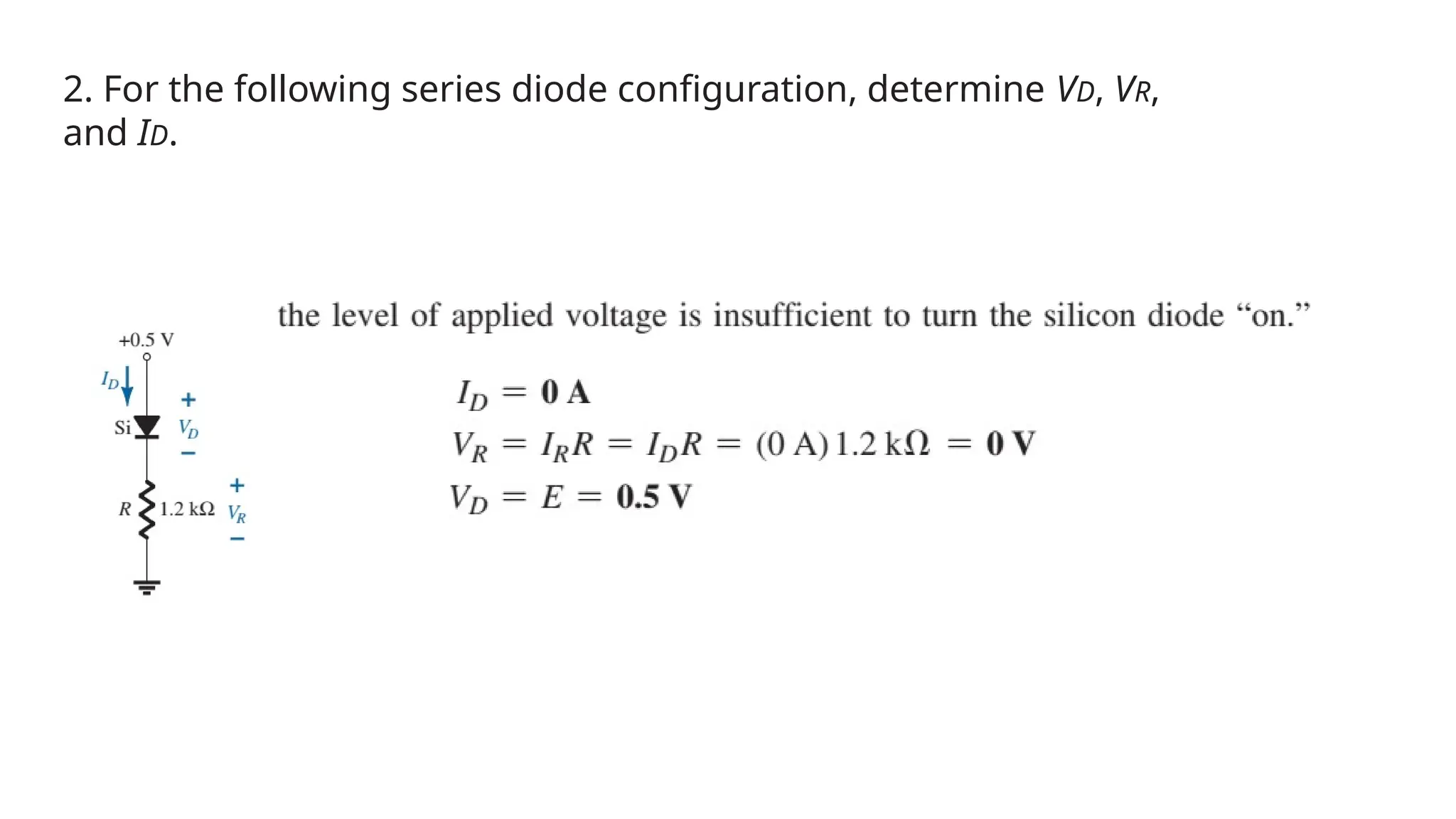
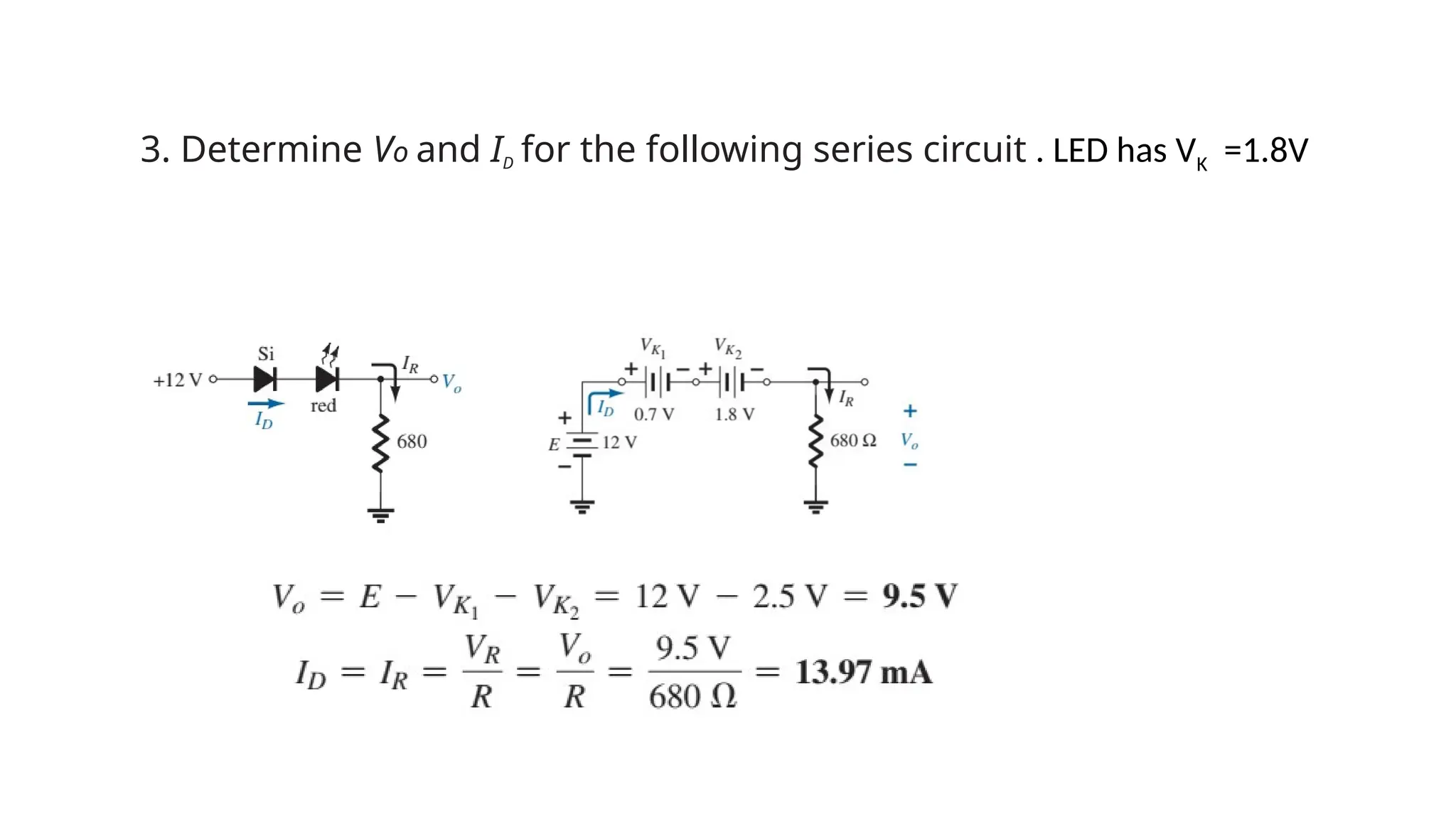
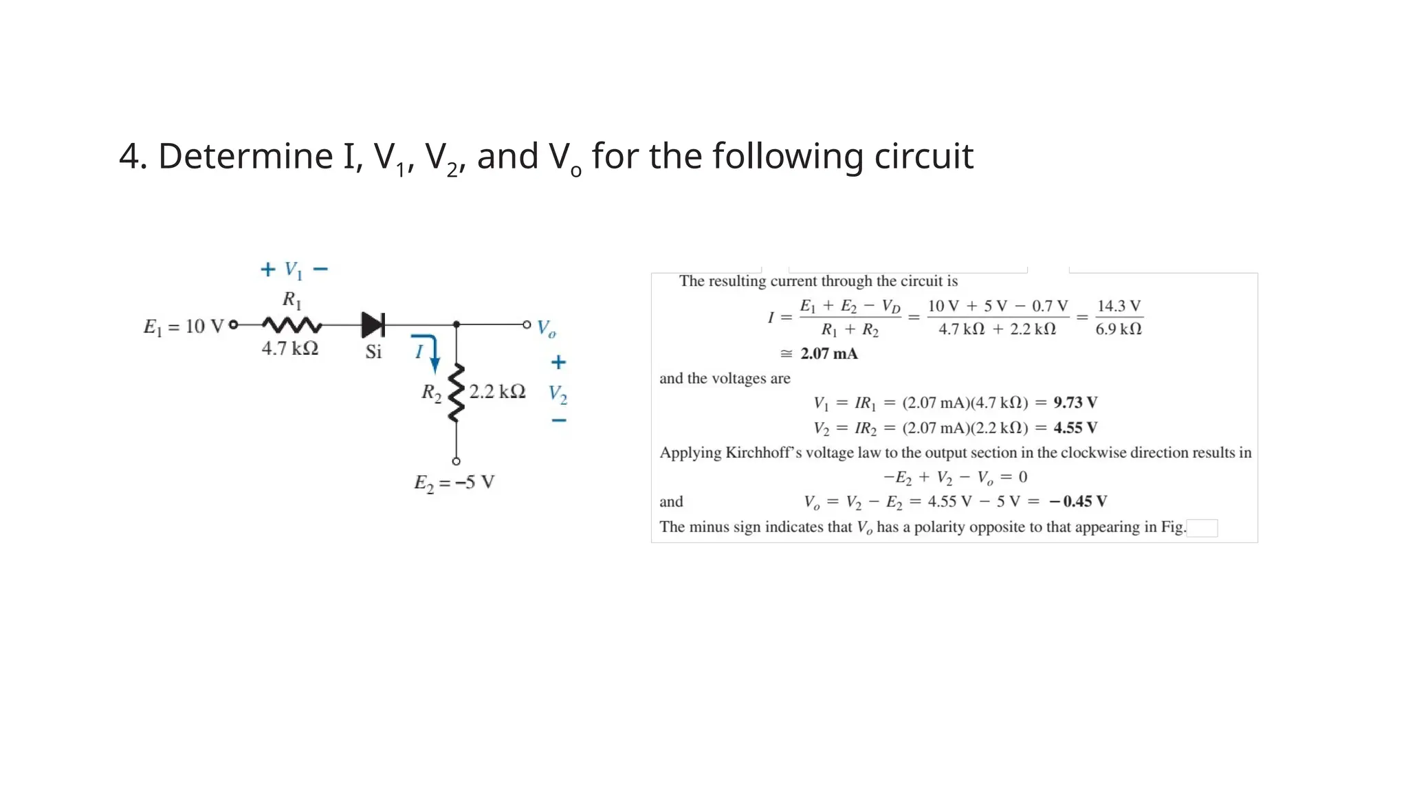
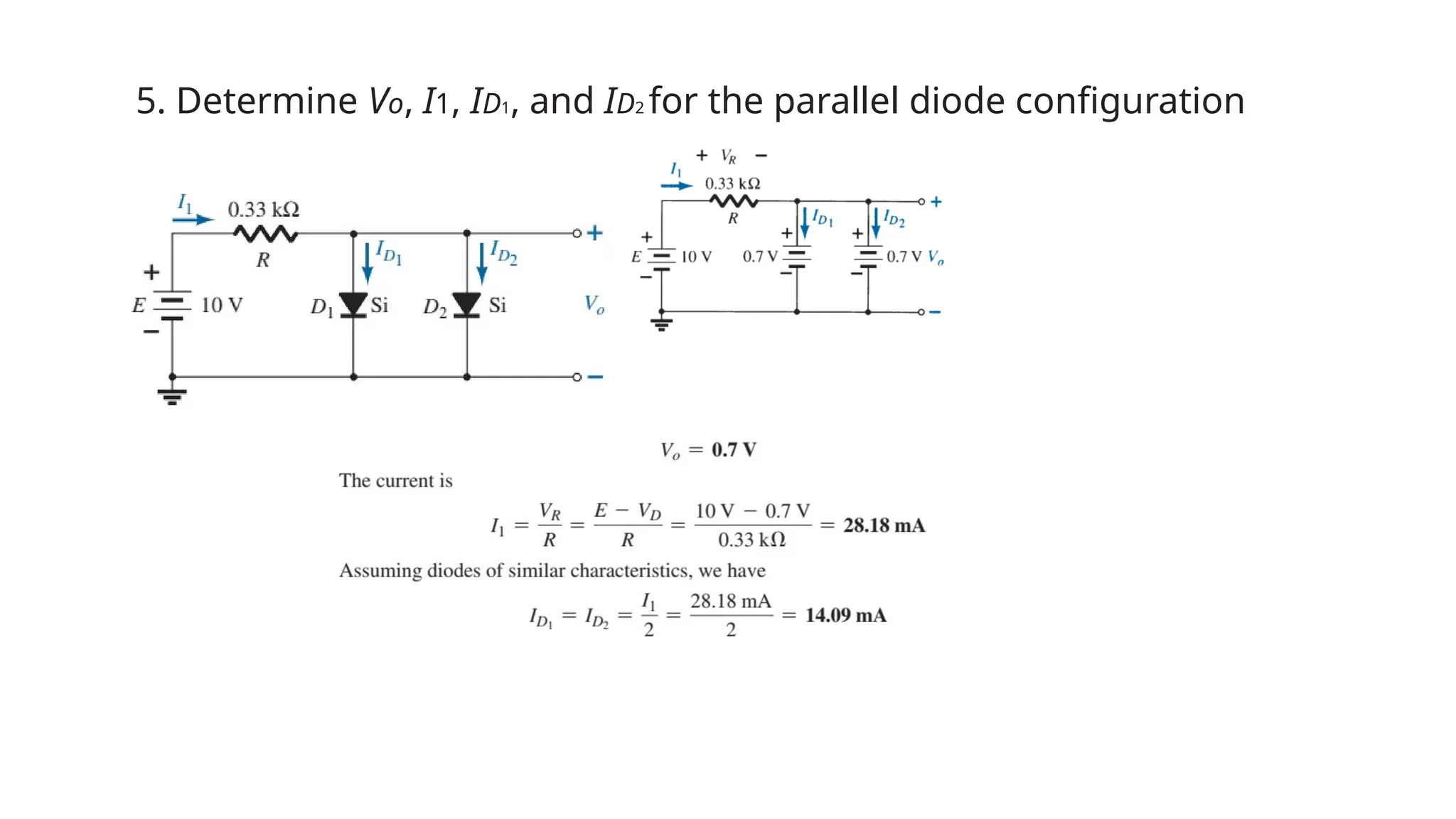
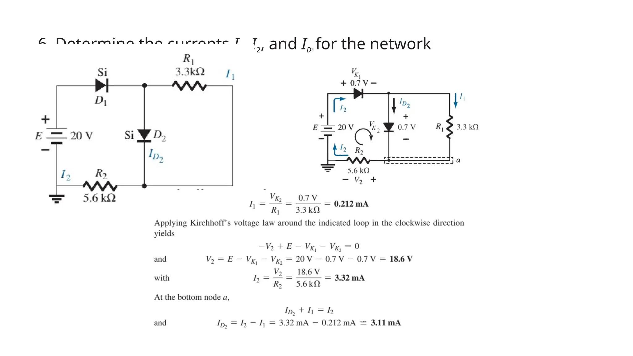
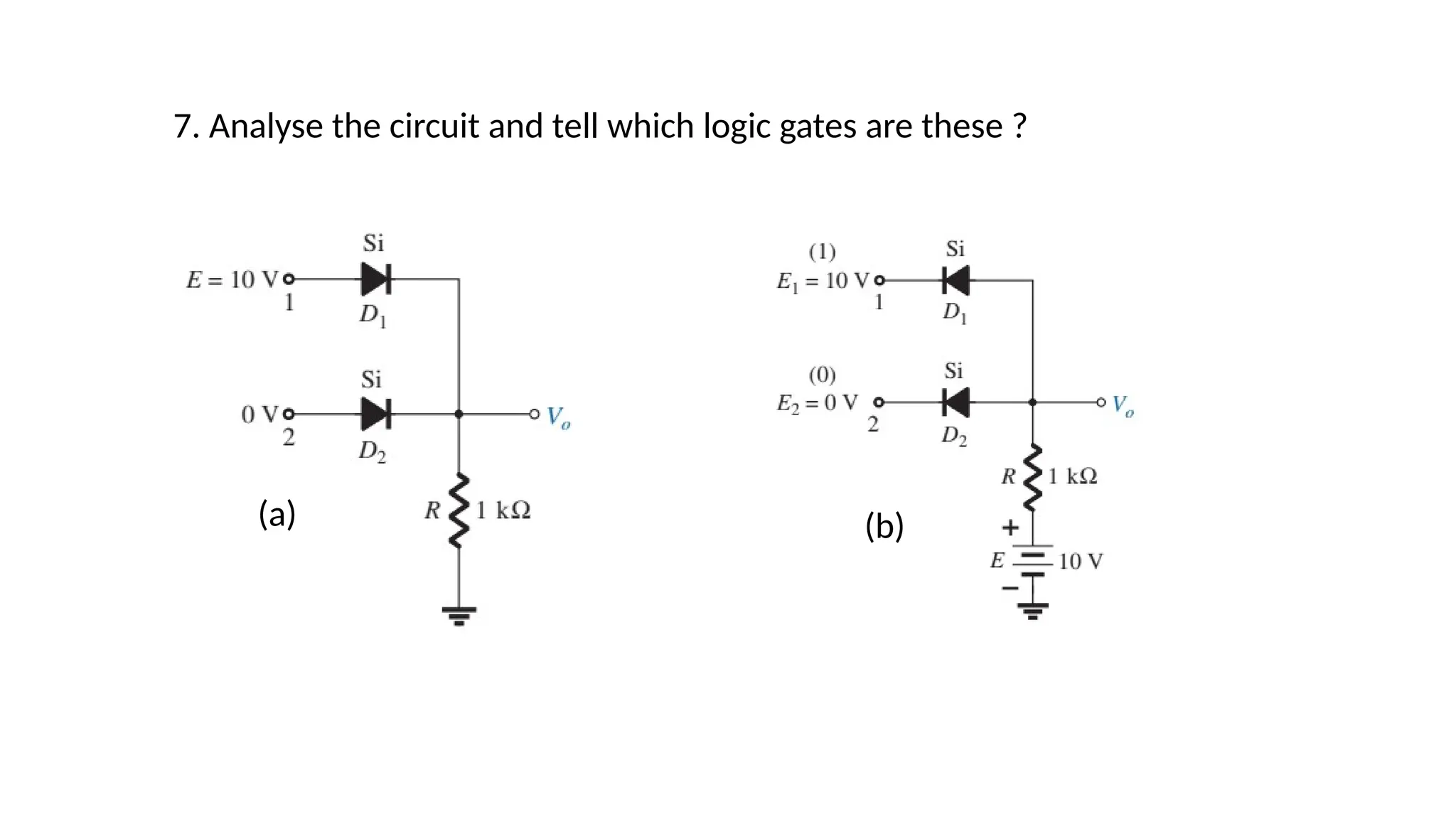
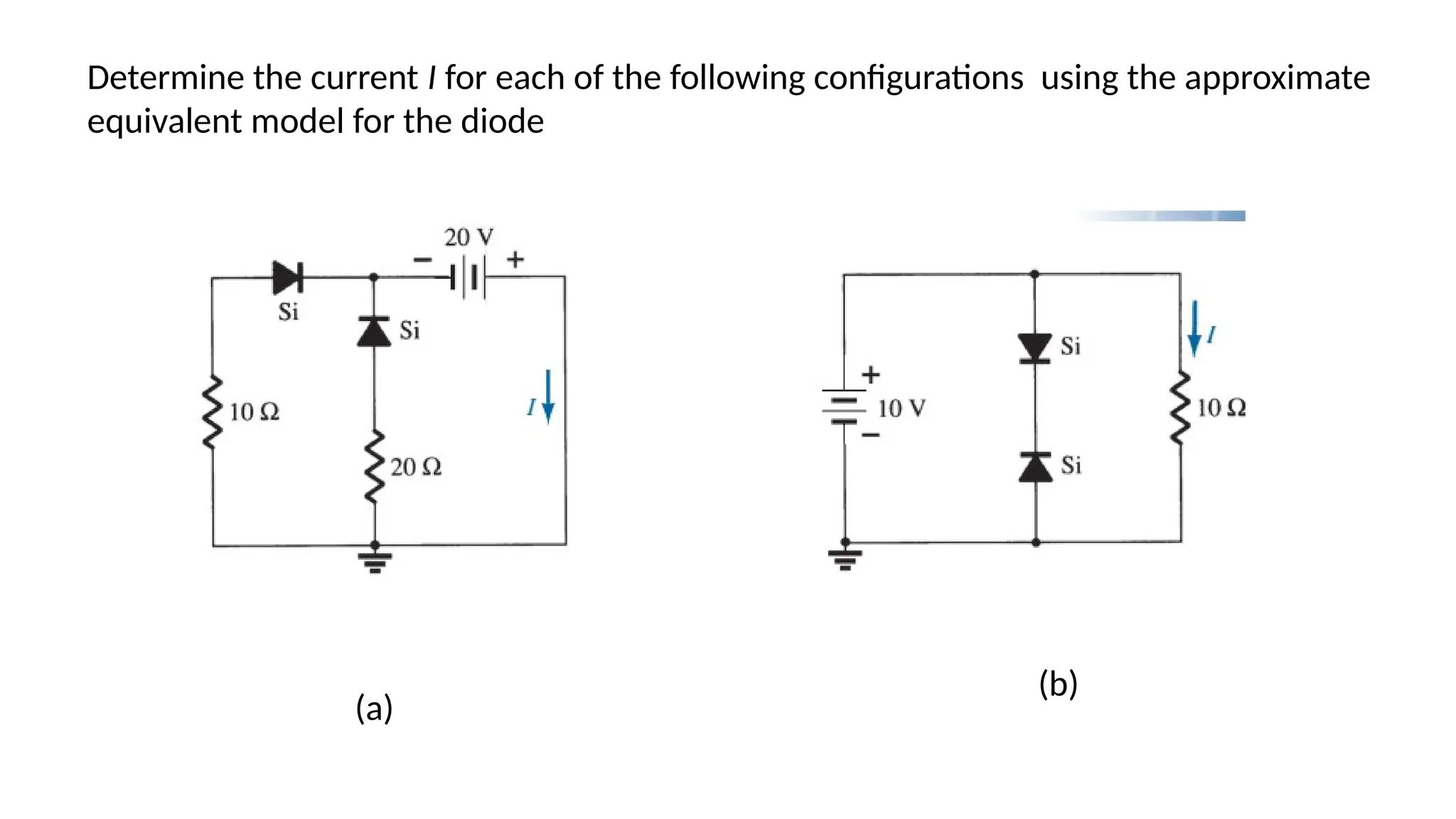
Electronics Devices and Circuits
(EC-1001)
भारतीय सूचना प्रौद्योगिकी संस्थान राँची
INDIAN INSTITUTE OF INFORMATION TECHNOLOGY, RANCHI
(An Institute of National Importance under act of Parliament)
Ranchi - 834004, Jharkhand
DIODE & APPLICATIONS
MODULE -2
Band Diagram Under Thermal Equilibrium
• Diode Characteristics
Shockley Equation
Diode Biasing
Forward bias
Diode Biasing (Forward bias)
• When a diode is connected in a Forward Bias condition, a negative voltage is applied to the N-type
material and a positive voltage is applied to the P-type material.
• If this external voltage becomes greater than the value of the potential barrier, approx. 0.7 volts for silicon
and 0.3 volts for germanium, the potential barriers opposition will be overcome and current will start to
flow.
• When the diode is forward biased, due to the negative terminal on the n-side, electrons from the n-side
are pushed towards the p-region.
• Similarly due to positive voltage on the P-side of the diode, Holes from the P-region are pushed towards N-
side.
• Due to this the electrons will start converting the positive ions in the P-region into neutral atoms and holes
will start converting the negative ions in the N-region to neutral atoms.
• Hence width of the depletion region starts reducing due to reduction in the barrier potential. So current to
flow from anode to cathode with little increase in the external voltage .
• The application of a forward biasing voltage on the junction diode results in the depletion layer becoming
very thin and narrow which represents a low impedance path through the junction thereby allowing high
currents to flow.
• The point at which this sudden increase in current takes place is represented on the static I-V
characteristics curve above as the "knee" point.
Reverse bias
Diode Biasing (Reverse bias)
• When a diode is connected in a Reverse Bias condition, a positive voltage is applied to the N-type material and a
negative voltage is applied to the P-type material.
• The positive voltage applied to the N-type material attracts electrons towards the positive electrode and away from the
junction, while the holes in the P-type end are also attracted away from the junction towards the negative electrode.
• The net result is that the depletion layer grows wider due to a lack of electrons and holes and presents a high
impedance path. The result is that a high potential barrier is created thus preventing current from flowing through the
semiconductor material.
• This condition represents a high resistance value to the PN junction and practically zero current flows through the
junction diode with an increase in bias voltage. However, a very small leakage current does flow through the junction
which can be measured in microamperes, (μA) (Saturation current).
• One final point, if the reverse bias voltage Vr applied to the diode is increased to a sufficiently high enough value, it will
cause the PN junction to overheat and fail due to the avalanche effect around the junction. This may cause the diode to
become shorted and will result in the flow of maximum circuit current, and this shown as a step downward slope in the
reverse static characteristics curve .
• Which lamps will glow in the following ckt. ?
NUMERICAL (DIODE CIRCUIT ANALYSIS)
MODULE -2
1. For the following series diode configuration, determine VD, VR, and ID.
2. For the following series diode configuration, determine VD, VR,
and ID.
3. Determine Vo and ID for the following series circuit . LED has VK =1.8V
4. Determine I, V1, V2, and Vo for the following circuit
5. Determine Vo, I1, ID1, and ID2 for the parallel diode configuration
6. Determine the currents I1, I2, and ID2 for the network
7. Analyse the circuit and tell which logic gates are these ?
(a) (b)
Determine the current I for each of the following configurations using the approximate
equivalent model for the diode
(a)
(b)

Diode operation and diode circuit analysis

  • 1.
    Electronics Devices andCircuits (EC-1001) भारतीय सूचना प्रौद्योगिकी संस्थान राँची INDIAN INSTITUTE OF INFORMATION TECHNOLOGY, RANCHI (An Institute of National Importance under act of Parliament) Ranchi - 834004, Jharkhand
  • 2.
  • 9.
    Band Diagram UnderThermal Equilibrium
  • 10.
    Band Diagram UnderThermal Equilibrium
  • 13.
  • 15.
  • 16.
  • 17.
    Diode Biasing (Forwardbias) • When a diode is connected in a Forward Bias condition, a negative voltage is applied to the N-type material and a positive voltage is applied to the P-type material. • If this external voltage becomes greater than the value of the potential barrier, approx. 0.7 volts for silicon and 0.3 volts for germanium, the potential barriers opposition will be overcome and current will start to flow. • When the diode is forward biased, due to the negative terminal on the n-side, electrons from the n-side are pushed towards the p-region. • Similarly due to positive voltage on the P-side of the diode, Holes from the P-region are pushed towards N- side. • Due to this the electrons will start converting the positive ions in the P-region into neutral atoms and holes will start converting the negative ions in the N-region to neutral atoms. • Hence width of the depletion region starts reducing due to reduction in the barrier potential. So current to flow from anode to cathode with little increase in the external voltage . • The application of a forward biasing voltage on the junction diode results in the depletion layer becoming very thin and narrow which represents a low impedance path through the junction thereby allowing high currents to flow. • The point at which this sudden increase in current takes place is represented on the static I-V characteristics curve above as the "knee" point.
  • 18.
  • 19.
    Diode Biasing (Reversebias) • When a diode is connected in a Reverse Bias condition, a positive voltage is applied to the N-type material and a negative voltage is applied to the P-type material. • The positive voltage applied to the N-type material attracts electrons towards the positive electrode and away from the junction, while the holes in the P-type end are also attracted away from the junction towards the negative electrode. • The net result is that the depletion layer grows wider due to a lack of electrons and holes and presents a high impedance path. The result is that a high potential barrier is created thus preventing current from flowing through the semiconductor material. • This condition represents a high resistance value to the PN junction and practically zero current flows through the junction diode with an increase in bias voltage. However, a very small leakage current does flow through the junction which can be measured in microamperes, (μA) (Saturation current). • One final point, if the reverse bias voltage Vr applied to the diode is increased to a sufficiently high enough value, it will cause the PN junction to overheat and fail due to the avalanche effect around the junction. This may cause the diode to become shorted and will result in the flow of maximum circuit current, and this shown as a step downward slope in the reverse static characteristics curve .
  • 30.
    • Which lampswill glow in the following ckt. ?
  • 31.
    • Which lampswill glow in the following ckt. ?
  • 32.
    NUMERICAL (DIODE CIRCUITANALYSIS) MODULE -2
  • 33.
    1. For thefollowing series diode configuration, determine VD, VR, and ID.
  • 34.
    2. For thefollowing series diode configuration, determine VD, VR, and ID.
  • 35.
    3. Determine Voand ID for the following series circuit . LED has VK =1.8V
  • 36.
    4. Determine I,V1, V2, and Vo for the following circuit
  • 37.
    5. Determine Vo,I1, ID1, and ID2 for the parallel diode configuration
  • 38.
    6. Determine thecurrents I1, I2, and ID2 for the network
  • 39.
    7. Analyse thecircuit and tell which logic gates are these ? (a) (b)
  • 40.
    Determine the currentI for each of the following configurations using the approximate equivalent model for the diode (a) (b)