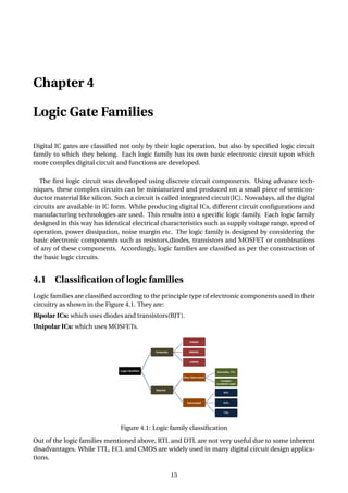
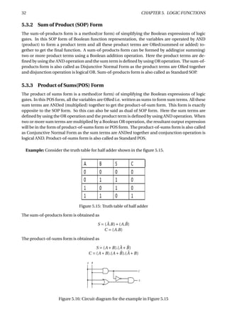
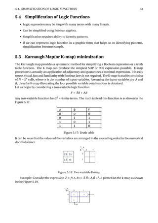
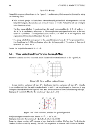
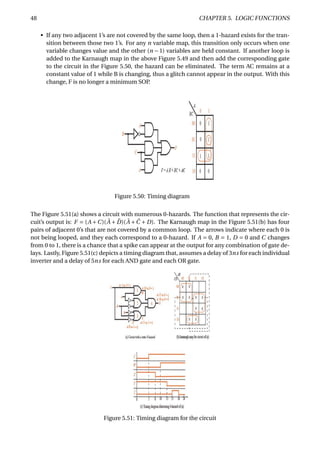
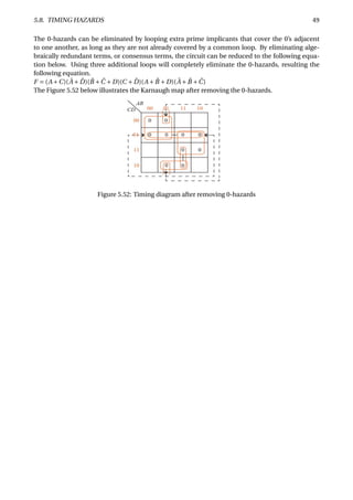
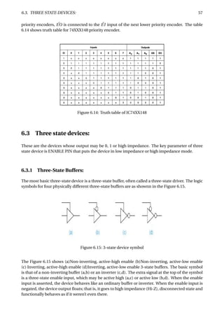
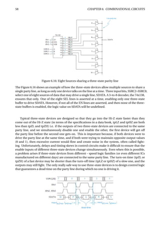
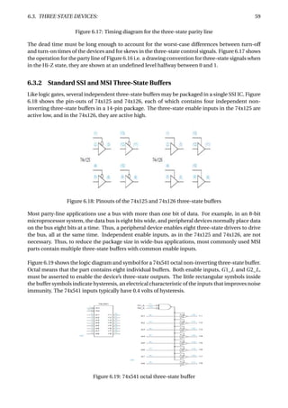
The document provides an overview of digital number systems and codes. It discusses binary, octal, hexadecimal, signed magnitude, one's complement, two's complement and excess representations. Binary is the base system for digital circuits due to its two voltage levels. Negative numbers can be represented using the sign bit in signed magnitude or by taking the complement. Two's complement is commonly used as it allows addition/subtraction of positive and negative numbers without checking signs.

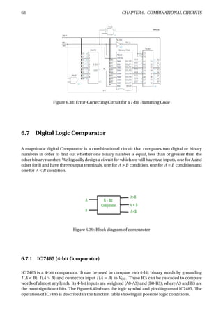
![6.6. EXCLUSIVE-OR GATES AND PARITY CHECKERS 67
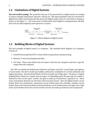
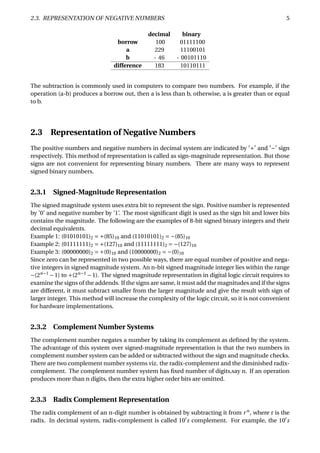
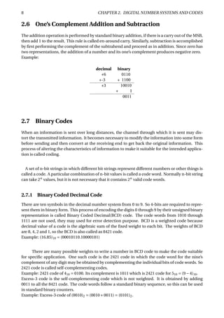
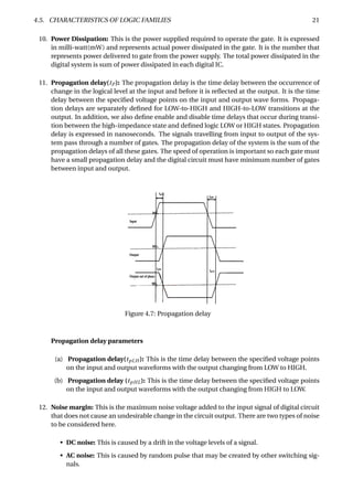
Figure 6.37: Parity generation and checking for an 8-bit-wide memory system
The Figure 6.37 shows how a parity circuit might be used to detect errors in the memory of a mi-
croprocessor system. The memory stores 8-bit bytes, plus a parity bit for each byte. The micropro-
cessor uses a bidirectional bus D[0:7] to transfer data to and from the memory. Two control lines,
RD and WR, are used to indicate whether a read or write operation is desired, and an ERROR signal
is asserted to indicate parity errors during read operations.
To store a byte into the memory chips, we specify an address (not shown), place the byte on D[0–7],
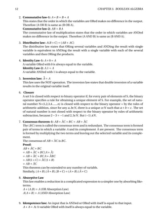
generate its parity bit on PIN, and assert WR. The AND gate on the I input of the 74x280 ensures
that I is 0 except during read operations, so that during writes the 74x280’s output depends only
on the parity of the D-bus data. The 74x280’s ODD output is connected to PIN, so that the total
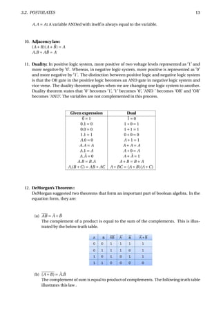
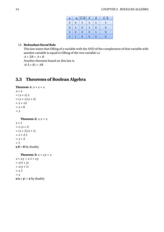
number of 1s stored is even.
To retrieve a byte, we specify an address (not shown) and assert RD. The byte value appears on
DOUT[0–7] and its parity appears on POUT. A 74x541 drives the byte onto the D bus, and the
74x280 checks its parity. If the parity of the 9-bit word DOUT[0–7], POUT is odd during a read, the
ERROR signal is asserted.
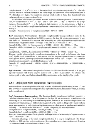
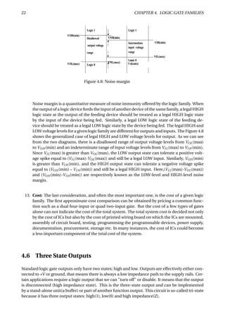
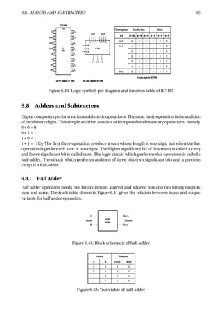
Parity circuits are also used with error-correcting codes such as the Hamming codes. We can cor-
rect errors in hamming code as shown in the Figure 6.38. A 7-bit word, possibly containing an
error, is presented on DU[1–7]. Three 74x280s compute the parity of the three bit-groups defined
by the parity-check matrix. The outputs of the 74x280s form the syndrome, which is the number
of the erroneous input bit, if any. A 74x138 is used to decode the syndrome. If the syndrome is
zero, the NOERROR_L signal is asserted (this signal also could be named ERROR). Otherwise, the
erroneous bit is corrected by complementing it. The corrected code word appears on the DC_L
bus.
Note: The active-low outputs of the 74x138 led us to use an active-low DC_L bus. If we required
an active-high DC bus, we could have put a discrete inverter on each XOR input or output, or used
a decoder with active-high outputs, or used XNOR gates.](https://image.slidesharecdn.com/ee224coursenotestill15-02-180223105314/85/Digital-Electronics-67-320.jpg)


![DE and LD [Autosave gyideffgfd] (1).pptx](https://cdn.slidesharecdn.com/ss_thumbnails/deandldautosaved1-241217121920-14134e9a-thumbnail.jpg?width=640&height=640&fit=bounds)


