Downloaded 30 times


![REFERENCES
[1] V. Barkhordarian, “Power MOSFET [14] “Transformer-Isolated Gate Driver
Basics”, International Rectifier, Technical Provides Very Large Duty Cycle Ratios”,
Paper International Rectifier, Application Note
[2] S. Clemente, et al., “Understanding AN-950B
HEXFET® Switching Performance”, [15] W. Andreycak, “Practical Considerations in
International Rectifier, Application Note Troubleshooting and Optimizing Power
947 Supply Control Circuits and PCB Layout”,
[3] B. R. Pelly, “A New Gate Charge Factor Unitrode Corporation, Power Supply
Leads to Easy Drive Design for Power Design Seminar, SEM-1200, Topic 4
MOSFET Circuits”, International Rectifier, [16] L. Spaziani, “A Study of MOSFET
Application Note 944A Performance in Processor Targeted Buck
[4] “Understanding MOSFET Data”, Supertex, and Synchronous Buck Converters”, HFPC
DMOS Application Note AN-D15 Power Conversion Conference, 1996, pp
[5] K. Dierberger, “Gate Drive Design For 123-137
Large Die MOSFETs”, PCIM ‘93, [17] W. Andreycak, “Practical Considerations
reprinted as Advanced Power Technology, In High Performance MOSFET, IGBT and
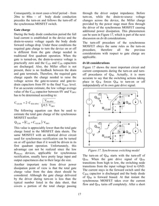
Application Note APT9302 MCT Gate Drive Circuits”, Unitrode
[6] D. Gillooly, “TC4426/27/28 System Corporation, Application Note U-137
Design Practice”, TelCom Semiconductor, [18] J. O’Connor, “Unique Chip Pair Simplifies
Application Note 25 Isolated High Side Switch Drive” Unitrode
[7] “Gate Drive Characteristics and Corporation, Application Note U-127
Requirements for HEXFET®s”, [19] D. Dalal, “Design Considerations for
International Rectifier, Application Note Active Clamp and Reset Technique”,
AN-937 Unitrode Corporation, Power Supply
[8] “TK75050 Smart MOSFET Driver Design Seminar SEM1100, Topic 3
Datasheet”, TOKO Power Conversion ICs [20] E. Wittenbreder, “Zero voltage switching
Databook, Application Information Section pulse width modulated power converters”,
[9] Adams, “Bootstrap Component Selection U.S. Patent No. 5402329.
For Control IC’s”, International Rectifier, [21] R. Erickson, “Lecture 20, The Transistor as
Design Tip DT 98-2 a Switching Device”, Power Electronics
[10] “HV Floating MOS-Gate Driver ICs”, ECE579 Course Notes, Fall 1987, pg. 20-4
International Rectifier, Application Note through 20-16.
INT978 [22] R. Severns, J. Armijos, “MOSFET
[11] C. Chey, J. Parry, “Managing Transients in Electrical Characteristics,” MOSPOWER
Control IC Driven Power Stages” Applications Handbook, Siliconix, Inc.,
International Rectifier, Design Tip DT 97-3 1984, pg. 3-1 through 3-8.
[12] “HIP408X Level Shifter Types”, Harris [23] J. Bliss, “The MOSFET Turn-Off Device -
Semiconductor A New Circuit Building Block,” Motorola
Semiconductor, Engineering Bulletin
[13] “IR2110 High and Low Side Driver” EB142, 1990.
International Rectifier, Data Sheet No. PD-
6.011E
37](https://image.slidesharecdn.com/mosfet-must-read-2-slup169-130412183116-phpapp02/85/Mosfet-must-read-2-slup169-37-320.jpg)

This document provides a guide to designing high-performance gate drive circuits for high-speed MOSFET switching applications. It discusses MOSFET technology and the gate drive requirements of power MOSFETs. The paper analyzes popular circuit solutions for gate drives and their performance. It describes design procedures for different types of gate drive circuits like ground referenced, high-side, AC coupled, and transformer isolated drives.