This one is an oldie, so please excuse the visual style. It comes from the first year of my PhD studies, 1994. The guidelines shown may still be of use to somebody working in printed circuit board (PCB) design. IT’S PROBABLY BEST DOWNLOADED since it's meant to run as a rolling slideshow, and it achieves a crude form of animations via multiple slides...
File translation courtesy of Zamzar.com, which allowed me to salvage this very old file, and make it available. For the PhD thesis itself (1999), see http://usir.salford.ac.uk/34320/
Our PCB 101 Presentation goes through the processes involved in manufacturing a printed circuit board.
From a simple single sided board to a complex multi-layer, double sided surface mount design, our goal is to provide you a design that meets your requirements and is the most cost effective to manufacture. Our experience in IPC Class III standards, very stringent cleanliness requirements, heavy copper and production tolerances allow us to provide our customers exactly what they need for their end product.
Prevent time-to-market delays by identifying manufacturing issues before they become a costly mistake. It’s not uncommon for designs to be submitted to manufacturing only to have problems identified that require design reworking and re-submission. This results in lost production time, schedule delays, and recurring tooling costs. What if you could identify DFM problems as you design and fix them when they happen? We will help show you how to spot and fix troublesome DFM issues in-design before they ever become a problem.
Based on on-demand webinar. Watch full recording here: https://resources.ema-eda.com/webinars/on-demand-webinar-design-for-manufacturing-dfm-and-why-it-matters
Project Report on SMT and through-hole technologylakshya bhardwaj
SMT and Through-hole technology and their assembly line, different types of Soldering, ESD protection, Conformal coating, etc, all about PCB Production
This presentation is intended to provide an introduction to the NDT method of penetrant testing. Penetrant Testing (PT) is a non destructive testing method that builds on the principle of Visual Inspection.
How to find defects in SMT electronics manufacturingBill Cardoso
This presentation covers several examples of defects found in today's SMT electronics manufacturing lines. Learn how x-rays can be used to find these defects, and most importantly, diagnose your manufacturing line.
All x-ray images taken with TruView X-Ray Inspection systems.
- Where Are Defects Introduced in the SMT production line?
- Solder Paste Application Defects
- Component Placement Defects
- Reflow Oven Defects
- Statistical Process Control
This training is very necessary to them who are working in Electronics manufacturing because Soldering process is the Heart of Electronics Industry, that's why this training is very important to employees.
A printed circuit board (PCB) mechanically supports and electrically connects electronic components using conductive tracks, pads and other features etched from copper sheets laminated onto a non-conductive substrate.
PCB stands for Printed Circuit Boards. HPCB PCB manufacturer specializes in prototype to medium production volumes. With our speedy and strong engineering support, we can provide simple solutions to complex design issues. Just simply send a Gerber file to us; we come back with the PCB of your choice with the stated time frame.
High Voltage PCB Design Presentation by AltiumAltium
Looking for High Voltage PCB design resources?
Take a look at Altium's resources for electrical engineers and PCB designers here.
Or view the original presentation at: https://resources.altium.com/presentations/high-voltage-pcb-design-presentation
Or for even more information on High Voltage PCB Design, click here:
https://resources.altium.com/pcb-design-blog/high-voltage-pcb-design-creepage-and-clearance-distance
Since 1997, RUSH PCB Inc. has been serving the electronics industry with printed circuit boards manufacturing and assembly services across the United States and globally. Our business is to manufacture boards from 2 to 32 layers, provide quick turn consigned and full turn-key assemblies.
Rush Pcb is the #1 pcb manufacturer in USA. Our services include pcb manufacturing, pcb fabrication, pcb
design and pcb assembly services.
objectives, applications, mechanism of size separation, the official standard of powders, sieves, sieve shaker, cyclone separator, air separator, bag filter, elutriation tank
System of Limits, Fits, Tolerance and GaugingTushar Makvana
To satisfy the ever-increasing demand for accuracy, the parts have to be produced with a less dimensional variation.
Hence, the labour and machinery required to manufacture a part has become more expensive.
It is essential for the manufacturer to have an in-depth knowledge of the tolerances to manufacture parts economically but, at the same time, adhere to quality and reliability aspects.
Moving to Manufacture: What Are You Producing? Designing Kits, Designing Printed circuit boards, Software Choices, The Design Process, Manufacturing Printed Circuit Boards, Etching Boards, Milling Boards. Assembly, Testing, Mass-Producing the Case and Other Fixtures, Certification, Costs, Scaling Up Software, Deployment, Correctness and Maintainability, Security, Performance, User Community. Ethics: Characterizing the Internet of Things, Privacy, Control, Disrupting Control, Crowdsourcing, Environment, Physical Thing, Electronics, Internet Service, Solutions, The Internet of Things as Part of the Solution, Cautious Optimism, The Open Internet of Things Definition.
Similar to Design for in-circuit test (vintage 1994) (20)
Pkyrete research project: interim presentationRichard Farr
This research project aimed to create ‘Environmentally Benign Containers’, exploring if the cold chain (for example, fish being transported in flaked ice) could employ reinforced ice – called Pkyrete – in place of styrofoam, to reduce the amount of single-use material going into landfill.
This presentation provides an introduction to the key concepts of the sustainable supply chain, providing definitions of sustainability, explaining climate change and the ways that supply chains can be expected to change in the future, as a result of the need to "go green".
Green design principles are introduced, including the need to avoid creating a "monstrous hybrid". The limitations of recycling are explained and the need for business models centred upon reuse is made clear. The presentation is designed for use at HE5 and HE6 (UK second year or final year Bachelors degree) but it could also be of interest to companies and individuals.
The slides are downloadable, and the download includes presenter notes – plus a short sustainability game that was used in class.
Get your classroom warmed up with this simple exercise, challenging students to decide and justify the location of a set of facilities. The slides are downloadable, and include teaching notes and a handout sheet for students to complete.
Richard Farr and Joe Gazdula: the Social Media Minefield, a presentation for the TIRI 2016 ("Teaching Intensive, Research Informed") conference. Looking at what social media might bring to the classroom... and discussing some of the hazards for educators.
Simulating the Impacts of RemanufacturingRichard Farr
It’s the billion-dollar industry that most people have never heard of: remanufacturing... taking products at the end of their life and making them as good as new (or better). Should businesses plan to get products back, renew them and make them serve again? That's complicated: the sustainability benefits of remanufacturing are obvious, but the consequences at the operational level include fluctuating capacity requirements, and a need for new skills within the organisation. A parametric model, described here, shows how a business might find out what they can expect if they pursue a remanufacturing strategy. Originally presented at ICoR 2011, the International Conference on Remanufacturing.
Supply Chain Management: Context, Collaboration and CompetitionRichard Farr
Why are supply chains as they are? Who decides what jobs a company should do, and which ones should be left to others? These slides encourage the learner to think about the company operations in their supply chain context, with reference to established principles such as Porter's Five Forces, and Brandenburger and Nalebuff's work on coopetition. Suggested student activities are included, and the presentation can be downloaded.
Assembly is often a neglected activity: human beings are clever, dexterous and adaptable, so all too often we leave the production worker to figure things out. Proper assembly planning would reduce risks, and save time and money. This presentation introduces the key concepts of assembly sequence generation and evaluation. It doesn’t promote any particular software tool, but provides an introduction to the types that exist, and makes a case for a systematic consideration of the assembly task. Review questions for learners are included.
Downloadable presentation in Powerpoint format, originally produced with Keynote.
Giving feedback to students is often mutually unsatisfactory: it requires a great deal of time, yet it isn't always accessed. Can we do something better? This presentation was used to kick off a practitioner workshop back in 2014.
Environmental Impact of Cruise HolidaysRichard Farr
What is the environmental impact of a cruise holiday? The authors used Life Cycle Assessment (LCA) – a technique more commonly found in manufacturing and engineering – to examine the carbon footprint of a cruise holiday, and compare this to a conventional hotel stay... finding that cruising is the 21st century equivalent of wearing fur: luxurious, but morally questionable!
Presented at “Contemporary Perspectives in Tourism and Hospitality Research: Policy, Practice and Performance” 12-14 July 2015, University of Brighton
Full paper available on ResearchGate: https://www.researchgate.net/publication/280008702_A_Life_Cycle_Assessment_of_the_Environmental_Impact_of_Cruise_Holidays
Design for Assembly (DFA) is a vital component of concurrent engineering – the multidisciplinary approach to product development. You might think it strange to begin by thinking about the assembly before you have designed all the components, but you can often eliminate many parts at the conceptual stage, and save yourself a lot of trouble.
This slideshow provides an introduction to the rules that are used in industry to produce affordable, reliable products. It includes the in-depth analysis of two real-world products subjected to a "product autopsy", detailed in photographs, plus tutor notes and recommendations for additional activities including an assembly game.
+++
Thanks for all the interest shown in this presentation... visit Capacify and leave me a message if you have any questions or comments. Also let me know if you'd like to have me as a guest speaker: the in-class 'ease of assembly game' is always fun.
Coopetition changes everything. Learn how to turn your competitors into 'complementors', and find "win-win" solutions in the modern business environment. Supported by examples, this short presentation explains the basic principles of how to secure a "bigger slice of the pie" even as you work to make the "pie" bigger for everybody.
The mantra of modern management in risk reduction, risk reduction, risk reduction... but what is risk, and how can managers make informed decisions about the hazards they (might) face? This presentation introduces students to some fundamental concepts, and methodologies, making reference to a boardgame that virtually everybody knows.
As a business, how can you reduce the impact of tourism, and ensure that you have access to visitor attractions for years to come? How can you defend yourself against critics, and how can you detect 'greenwash'? Finally, students apply what has been covered by planning a sustainable holiday.
You design for manufacture, design for assembly, design for reliability... why not design for logistics as well?
This presentation provides a theoretical background on the purposes of packaging, and the characteristics of products with good logistics properties. The efficiency of packaging strategies is discussed, and the influence of good relationships within the supply chain.
How can the complex supply chain for an aero engine respond to a request for quotation from an airline in just a week? This is the presentation that accompanied our ICE 2006 conference paper on aero industry virtual enterprises, legal issues and the "seven day proposal". One output from the EU Sixth Framework Integrated Project, VIVACE (Value Improvement through a VIRTUAL Aerospace Collaborative Enterprise).
Uses the ‘Da Vinci’ theme from Keynote Theme Park.
We are the stakeholders. All of us: you, me, governments, businesses and host communities... what happens in the tourism industry affects us all. This introductory lecture presents some of the key concepts in sustainable tourism, and reviews some of the problems that we face.
Don't let the natural and cultural wonders of our world be degraded by the people who love them and want to experience them: instead, discover sustainable solutions that benefit everyone.
Impacts of Cruise Tourism upon Small Island CommunitiesRichard Farr
Cruise holidays: love them or hate them... you can't deny that there are more people cruising than ever before. But is cruising ethical? Sustainable? Using the emerging destination of Chios as an example, we look at the impact that cruise ships have upon port communities, and the natural environment.
This is the conference presentation that accompanied our first research paper on the impact of cruise tourism, looking at a small island community in the Aegean.
For the full text of the accompanying paper, see: http://www.jotr.eu/index.php/tourism-management/64-understanding
Industrial Training at Shahjalal Fertilizer Company Limited (SFCL)MdTanvirMahtab2
This presentation is about the working procedure of Shahjalal Fertilizer Company Limited (SFCL). A Govt. owned Company of Bangladesh Chemical Industries Corporation under Ministry of Industries.
Water scarcity is the lack of fresh water resources to meet the standard water demand. There are two type of water scarcity. One is physical. The other is economic water scarcity.
Sachpazis:Terzaghi Bearing Capacity Estimation in simple terms with Calculati...Dr.Costas Sachpazis
Terzaghi's soil bearing capacity theory, developed by Karl Terzaghi, is a fundamental principle in geotechnical engineering used to determine the bearing capacity of shallow foundations. This theory provides a method to calculate the ultimate bearing capacity of soil, which is the maximum load per unit area that the soil can support without undergoing shear failure. The Calculation HTML Code included.
Cosmetic shop management system project report.pdfKamal Acharya
Buying new cosmetic products is difficult. It can even be scary for those who have sensitive skin and are prone to skin trouble. The information needed to alleviate this problem is on the back of each product, but it's thought to interpret those ingredient lists unless you have a background in chemistry.
Instead of buying and hoping for the best, we can use data science to help us predict which products may be good fits for us. It includes various function programs to do the above mentioned tasks.
Data file handling has been effectively used in the program.
The automated cosmetic shop management system should deal with the automation of general workflow and administration process of the shop. The main processes of the system focus on customer's request where the system is able to search the most appropriate products and deliver it to the customers. It should help the employees to quickly identify the list of cosmetic product that have reached the minimum quantity and also keep a track of expired date for each cosmetic product. It should help the employees to find the rack number in which the product is placed.It is also Faster and more efficient way.
NO1 Uk best vashikaran specialist in delhi vashikaran baba near me online vas...Amil Baba Dawood bangali
Contact with Dawood Bhai Just call on +92322-6382012 and we'll help you. We'll solve all your problems within 12 to 24 hours and with 101% guarantee and with astrology systematic. If you want to take any personal or professional advice then also you can call us on +92322-6382012 , ONLINE LOVE PROBLEM & Other all types of Daily Life Problem's.Then CALL or WHATSAPP us on +92322-6382012 and Get all these problems solutions here by Amil Baba DAWOOD BANGALI
#vashikaranspecialist #astrologer #palmistry #amliyaat #taweez #manpasandshadi #horoscope #spiritual #lovelife #lovespell #marriagespell#aamilbabainpakistan #amilbabainkarachi #powerfullblackmagicspell #kalajadumantarspecialist #realamilbaba #AmilbabainPakistan #astrologerincanada #astrologerindubai #lovespellsmaster #kalajaduspecialist #lovespellsthatwork #aamilbabainlahore#blackmagicformarriage #aamilbaba #kalajadu #kalailam #taweez #wazifaexpert #jadumantar #vashikaranspecialist #astrologer #palmistry #amliyaat #taweez #manpasandshadi #horoscope #spiritual #lovelife #lovespell #marriagespell#aamilbabainpakistan #amilbabainkarachi #powerfullblackmagicspell #kalajadumantarspecialist #realamilbaba #AmilbabainPakistan #astrologerincanada #astrologerindubai #lovespellsmaster #kalajaduspecialist #lovespellsthatwork #aamilbabainlahore #blackmagicforlove #blackmagicformarriage #aamilbaba #kalajadu #kalailam #taweez #wazifaexpert #jadumantar #vashikaranspecialist #astrologer #palmistry #amliyaat #taweez #manpasandshadi #horoscope #spiritual #lovelife #lovespell #marriagespell#aamilbabainpakistan #amilbabainkarachi #powerfullblackmagicspell #kalajadumantarspecialist #realamilbaba #AmilbabainPakistan #astrologerincanada #astrologerindubai #lovespellsmaster #kalajaduspecialist #lovespellsthatwork #aamilbabainlahore #Amilbabainuk #amilbabainspain #amilbabaindubai #Amilbabainnorway #amilbabainkrachi #amilbabainlahore #amilbabaingujranwalan #amilbabainislamabad
Overview of the fundamental roles in Hydropower generation and the components involved in wider Electrical Engineering.
This paper presents the design and construction of hydroelectric dams from the hydrologist’s survey of the valley before construction, all aspects and involved disciplines, fluid dynamics, structural engineering, generation and mains frequency regulation to the very transmission of power through the network in the United Kingdom.
Author: Robbie Edward Sayers
Collaborators and co editors: Charlie Sims and Connor Healey.
(C) 2024 Robbie E. Sayers
Immunizing Image Classifiers Against Localized Adversary Attacksgerogepatton
This paper addresses the vulnerability of deep learning models, particularly convolutional neural networks
(CNN)s, to adversarial attacks and presents a proactive training technique designed to counter them. We
introduce a novel volumization algorithm, which transforms 2D images into 3D volumetric representations.
When combined with 3D convolution and deep curriculum learning optimization (CLO), itsignificantly improves
the immunity of models against localized universal attacks by up to 40%. We evaluate our proposed approach
using contemporary CNN architectures and the modified Canadian Institute for Advanced Research (CIFAR-10
and CIFAR-100) and ImageNet Large Scale Visual Recognition Challenge (ILSVRC12) datasets, showcasing
accuracy improvements over previous techniques. The results indicate that the combination of the volumetric
input and curriculum learning holds significant promise for mitigating adversarial attacks without necessitating
adversary training.
Saudi Arabia stands as a titan in the global energy landscape, renowned for its abundant oil and gas resources. It's the largest exporter of petroleum and holds some of the world's most significant reserves. Let's delve into the top 10 oil and gas projects shaping Saudi Arabia's energy future in 2024.
Hierarchical Digital Twin of a Naval Power SystemKerry Sado
A hierarchical digital twin of a Naval DC power system has been developed and experimentally verified. Similar to other state-of-the-art digital twins, this technology creates a digital replica of the physical system executed in real-time or faster, which can modify hardware controls. However, its advantage stems from distributing computational efforts by utilizing a hierarchical structure composed of lower-level digital twin blocks and a higher-level system digital twin. Each digital twin block is associated with a physical subsystem of the hardware and communicates with a singular system digital twin, which creates a system-level response. By extracting information from each level of the hierarchy, power system controls of the hardware were reconfigured autonomously. This hierarchical digital twin development offers several advantages over other digital twins, particularly in the field of naval power systems. The hierarchical structure allows for greater computational efficiency and scalability while the ability to autonomously reconfigure hardware controls offers increased flexibility and responsiveness. The hierarchical decomposition and models utilized were well aligned with the physical twin, as indicated by the maximum deviations between the developed digital twin hierarchy and the hardware.
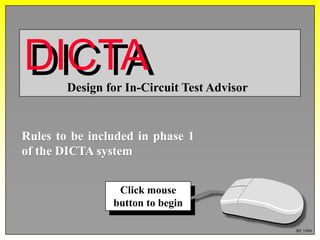
1. Design for In-Circuit Test Advisor
DICTADICTA
Rules to be included in phase 1
of the DICTA system
Click mouse
button to begin
RF 1994
2. Component Mounting
• Preferably, all components will be on the top side
of the circuit board
• Chip resistors and other small components can be
placed on the secondary side of the board, but they
must be located away from test pads
• Any flying wires should be located on the top side
of the PCB, away from test probes
best - all components on one side of the PCB
moderate - passives only on underside
worst - both sides
populated with ICs
3. Board Shape
• To facilitate sealing for vacuum fixturing, boards
should have straight sides and no internal cut-outs
• Any cut-outs must be surrounded by an area clear
of all obstructions.
Bad shapeLess good
shape
Good shape
4. Edge Clearance
• An area around the board perimeter should be free of
components, test locations and other features
• This should extend for at least 0.100, and preferably
0.200 inches from any edges or cut-outs
Clamping or sealing the board
edge becomes difficult
6. Locating Tooling Holes
• Tooling holes should be provided on at least two
opposite corners
• If space allows, a tooling hole on a third corner
will improve accuracy
• Holes should be offset so the board cannot be
placed in a fixture the wrong way round
• All tooling holes must be unplated
• Minimum diameter is 0.125 inches
7. Board Thickness
• To avoid distortion during testing, the board
should have a minimum thickness of 0.062 inches
8. Board Thickness
• To avoid distortion during testing, the board
should have a minimum thickness of 0.062 inches
16. Via Holes
• To ensure a reliable vacuum seal between the
assembled PCB and the test fixture, via holes
should be of sufficient diameter (0.062 inches or
more) so they will fill during flow soldering.
Likely to fill Unlikely to fill
17. Component Height
• Components on the bottom side of the board must
not obstruct the operation of the bed-of-nails fixture
• It is best if components have heights of less than
0.160 inches
• No components with heights greater than 0.360
inches should be mounted on the bottom of the
board
18. Component Height
• Components on the bottom side of the board must
not obstruct the operation of the bed-of-nails fixture
• It is best if components have heights of less than
0.160 inches
• No components with heights greater than 0.360
inches should be mounted on the bottom of the
board
Cut-out in top
plate required
Recess in vacuum
well required
Testability
unimpared
19. 60 mil
Component / Test Land Spacing
• The space between the centre of a test access point
and the edges of any adjacent components must
exceed 0.060 inches
• This distance must be increased to 0.200 inches
where the height of adjacent components exceeds
0.160 inches
200 mil
20. Test Land Size
• Test lands should be as large
as possible to ensure reliable
probing
• Recommended size is
greater than 0.060 inches
• Minimum size is 0.035
inches for a bed-of-nails
type fixture
• If the PCB requires two-
sided probing, the minimum
size for test lands on the top
side is 0.040 because
probing here is less accurate
21. Test Land Size
• Test lands should be as large
as possible to ensure reliable
probing
• Recommended size is
greater than 0.060 inches
• Minimum size is 0.035
inches for a bed-of-nails
type fixture
• If the PCB requires two-
sided probing, the minimum
size for test lands on the top
side is 0.040 because
probing here is less accurate
22. Test Land Size
• Test lands should be as large
as possible to ensure reliable
probing
• Recommended size is
greater than 0.060 inches
• Minimum size is 0.035
inches for a bed-of-nails
type fixture
• If the PCB requires two-
sided probing, the minimum
size for test lands on the top
side is 0.040 because
probing here is less accurate
23. Test Land Size
• Test lands should be as large
as possible to ensure reliable
probing
• Recommended size is
greater than 0.060 inches
• Minimum size is 0.035
inches for a bed-of-nails
type fixture
• If the PCB requires two-
sided probing, the minimum
size for test lands on the top
side is 0.040 because
probing here is less accurate
24. Test Land Size
• Test lands should be as large
as possible to ensure reliable
probing
• Recommended size is
greater than 0.060 inches
• Minimum size is 0.035
inches for a bed-of-nails
type fixture
• If the PCB requires two-
sided probing, the minimum
size for test lands on the top
side is 0.040 because
probing here is less accurate
25. Test Land Size
• Test lands should be as large
as possible to ensure reliable
probing
• Recommended size is
greater than 0.060 inches
• Minimum size is 0.035
inches for a bed-of-nails
type fixture
• If the PCB requires two-
sided probing, the minimum
size for test lands on the top
side is 0.040 because
probing here is less accurate
Small test pads may
well be missed as
probes wear
26. Land Spacing
• Test access points should be spaced with 0.100
inches between centres
• This can be reduced to 0.075 or even 0.050 where
necessary
• The number of probes at smaller pitches should be
kept to a minimum as these are less accurate
27. End of phase 1 rules
Other information to be included in the multimedia
design advisory system follows...
Click mouse button
to begin
Click mouse button
to continue
28. Board Probing
• If possible the board should be probed from one
side only
29. Board Probing
• If probing from both
sides of the board is
necessary it will be
found that probing
accuracy is reduced
on the top side
• The location of tall
components may also
make testing difficult.
30. Board Probing
• If probing from both
sides of the board is
necessary it will be
found that probing
accuracy is reduced
on the top side
• The location of tall
components may also
make testing difficult.
31. Board Probing
• If probing from both
sides of the board is
necessary it will be
found that probing
accuracy is reduced
on the top side
• The location of tall
components may also
make testing difficult.
32. Board Probing
• If probing from both
sides of the board is
necessary it will be
found that probing
accuracy is reduced
on the top side
• The location of tall
components may also
make testing difficult.
33. Board Probing
• If probing from both
sides of the board is
necessary it will be
found that probing
accuracy is reduced
on the top side
• The location of tall
components may also
make testing difficult.
34. Board Probing
• If probing from both
sides of the board is
necessary it will be
found that probing
accuracy is reduced
on the top side
• The location of tall
components may also
make testing difficult.
35. Component Orientation
• All packages of the same style should have the
same orientation so that time will not be wasted
trying to identify pins during manual testing
• Clear, permanent marking of pin numbering for
each component is also necessary
1
14
36. Probing Components
• Avoid probing the leads of the components
• Probing component leads can mask problems with
bad solder joints
• Test pads should be included in the design instead
37. Probing Components
• Avoid probing the leads of the components
• Probing component leads can mask problems with
bad solder joints
• Test pads should be included in the design instead
joint closed
by probe
38. Probing Components
• Avoid probing the leads of the components
• Probing component leads can mask problems with
bad solder joints
• Test pads should be included in the design instead
joint closed
by probe
39. Probing Components
• Avoid probing the leads of the components
• Probing component leads can mask problems with
bad solder joints
• Test pads should be included in the design instead
joint closed
by probe
40. Test Land Geometry
• Square test pads offer a greater area to hit so the
testing process is more reliable
Square pad
offers 27%
greater contact
area.
41. Test Land Geometry
• Solder on test pads may make probing difficult
• Mounting pads and test pads should be separated to
prevent solder flowing onto the test pad during
manufacture
• This also ensures the test probe will not strike a
component skewed during placement or reflow
Good Bad
42. Edge Connectors
• In terms of testabiity, the best design for testing
would achieve all the necessary contacts for
testing at the edge connectors
55. Test Probes
• Available in a variety of
sizes and head
configurations
• Larger probes have a
longer reach but may not
be practical in fine pitch
applications
plunger
wire wrap
connection
spring
barrel
fixture
head
56. Test Probes
• Available in a variety of
sizes and head
configurations.
• Larger probes have a
longer reach but may not
be practical in fine pitch
applications.
57. Test Probes
• Available in a variety of
sizes and head
configurations.
• Larger probes have a
longer reach but may not
be practical in fine pitch
applications.
58. Test Probes
• Available in a variety of
sizes and head
configurations.
• Larger probes have a
longer reach but may not
be practical in fine pitch
applications.
59. Test Probes
• Available in a variety of
sizes and head
configurations.
• Larger probes have a
longer reach but may not
be practical in fine pitch
applications.
60. Test Probes
• Available in a variety of
sizes and head
configurations.
• Larger probes have a
longer reach but may not
be practical in fine pitch
applications.
61. Test Probes
• Available in a variety of
sizes and head
configurations.
• Larger probes have a
longer reach but may not
be practical in fine pitch
applications.
62. Test Probes
• Available in a variety of
sizes and head
configurations.
• Larger probes have a
longer reach but may not
be practical in fine pitch
applications.
63. Test Probes
• Available in a variety of
sizes and head
configurations.
• Larger probes have a
longer reach but may not
be practical in fine pitch
applications.
64. Test Probes
• A large probe should be
used where possible for
better electrical contact
and improved fixture
reliability.
• Smaller probes must be
used where the test pads
are closely packed or
access is a problem.
65. Design for In-Circuit Test Advisor
DICTADICTA
End of slideshow. Click
mouse button to restart.