Downloaded 33 times

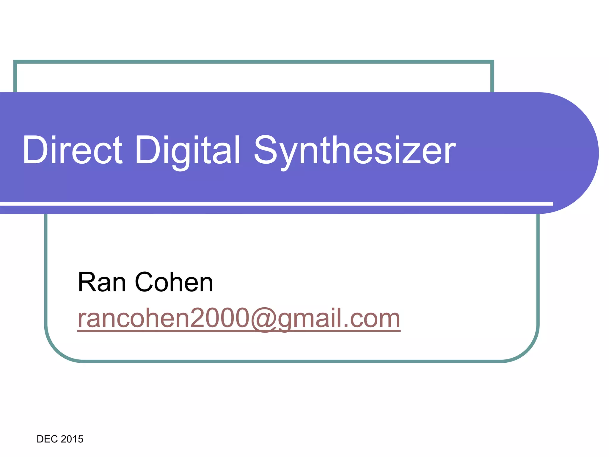
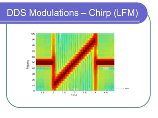
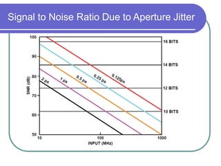
![Phase Offset Calculation
2
2
N
outPhase
POW round
2
2
out N
POW
Phase
MSB
LSB
Phase
Offset Word
Phase Out
[Deg]
Weight
BIT13 180 1/2
BIT12 90 1/4
BIT11 45 1/8
BIT10 22.5 1/16
BIT9 11.25 1/32
BIT8 5.625 1/64
BIT7 2.8125 1/128
BIT6 1.40625 1/256
BIT5 0.703125 1/512
BIT4 0.351563 1/1024
BIT3 0.175781 1/2048
BIT2 0.087891 1/4096
BIT1 0.043945 1/8192
BIT0 0.021973 1/16384
2 SECN
out
POW
Delay
f
](https://image.slidesharecdn.com/dds2016-170605194115/85/DDS-How-It-Works-8-320.jpg)
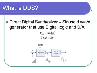
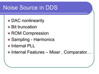
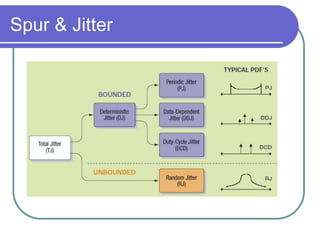
![Frequency Calculation
REF CLK 640 (MHz)
DFTW
Frequency Out
[MHz]
Weight
BIT32 320 1/2
BIT31 160 1/4
BIT30 80 1/8
BIT29 40 1/16
BIT28 20 1/32
BIT27 10 1/64
BIT26 5 1/128
BIT25 2.5 1/256
BIT24 1.25 1/512
BIT23 0.625 1/1024
BIT22 0.3125 1/2048
BIT21 0.15625 1/4096
BIT20 0.078125 1/8192
BIT19 0.0390625 1/16384
BIT18 0.01953125 1/32768
BIT17 0.009765625 1/65536
BIT16 0.004882813 1/131072
BIT15 0.002441406 1/262144
BIT14 0.001220703 1/524288
BIT13 0.000610352 1/1048576
BIT12 0.000305176 1/2097152
BIT11 0.000152588 1/4194304
BIT10 7.62939E-05 1/8388608
BIT9 3.81470E-05 1/16777216
BIT8 1.90735E-05 1/33554432
BIT7 9.53674E-06 1/67108864
BIT6 4.76837E-06 1/134217728
BIT5 2.38419E-06 1/268435456
BIT4 1.19209E-06 1/536870912
BIT3 5.96046E-07 1/1073741824
BIT2 2.98023E-07 1/2147483648
BIT1 1.49012E-07 1/4294967296
BIT0 7.45058E-08 1/8589934592
2
sys_clk
M
outf
FTW round
sys_clk
2
out M
FTW
f
MSB
LSB](https://image.slidesharecdn.com/dds2016-170605194115/85/DDS-How-It-Works-9-320.jpg)
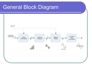
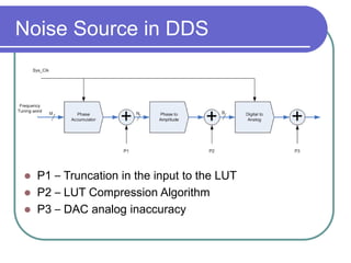
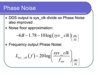
![0.0
0.2
0.4
0.6
0.8
1.0
1.2
1.4
1.6
1.8
2.0
0 1 2 3 4 5 6 7 8 9 10 11 12 13 14 15
0.0
0.2
0.4
0.6
0.8
1.0
1.2
1.4
1.6
1.8
2.0
0 1 2 3 4 5 6 7 8 9 10 11 12 13 14 15
FTW to Fout – 10 MHz
Phase
Acc.
Phase Sinuous
Sinuous
+ DC
D/A
Norm.
Lookup
Table
0 0 0 0.9 0.875 7
1 π/8 0.3827 1.2444 1.25 10
2 2π/8 0.7071 1.5364 1.5 12
3 3π/8 0.9239 1.7315 1.75 14
4 4π/8 1- 1.8 1.75 14
5 5π/8 0.9239 1.7315 1.75 14
6 6π/8 0.7071 1.5364 1.5 12
7 7π/8 0.3827 1.2444 1.25 10
8 π 0 0.9 0.875 7
9 9π/8 0.3827 0.5556 0.5 4
10 10π/8 0.7071 0.2636 0.25 2
11 11π/8 0.9239 0.0685 0.125 1
12 12π/8 -1 0 0 0
13 13π/8 0.9239 0.0685 0.125 1
14 14π/8 0.7071 0.2636 0.25 2
15 15π/8 0.3827 0.5556 0.625 5
6.25nsec
6.25nsec * 16 = 100 nsec (10MHz)
REF CLK 160(MHz)
DFTW
Frequency Out
[MHz]
Weight
BIT3 80 1/2
BIT2 40 1/4
BIT1 20 1/8
BIT0 10 1/16
MSB
LSB](https://image.slidesharecdn.com/dds2016-170605194115/85/DDS-How-It-Works-10-320.jpg)
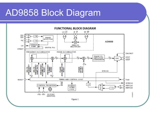
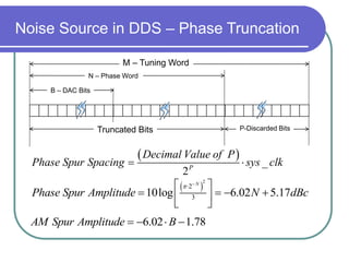
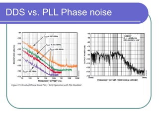
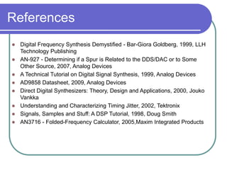
![0.0
0.2
0.4
0.6
0.8
1.0
1.2
1.4
1.6
1.8
2.0
0 1 2 3 4 5 6 7 8 9 10 11 12 13 14 15
FTW to Fout – 40 MHz
Phase
Acc.
Phase Sinuous
Sinuous
+ DC
D/A
Norm.
Lookup
Table
0 0 0 0.9 0.875 7
1 π/8 0.3827 1.2444 1.25 10
2 2π/8 0.7071 1.5364 1.5 12
3 3π/8 0.9239 1.7315 1.75 14
4 4π/8 1- 1.8 1.75 14
5 5π/8 0.9239 1.7315 1.75 14
6 6π/8 0.7071 1.5364 1.5 12
7 7π/8 0.3827 1.2444 1.25 10
8 π 0 0.9 0.875 7
9 9π/8 0.3827 0.5556 0.5 4
10 10π/8 0.7071 0.2636 0.25 2
11 11π/8 0.9239 0.0685 0.125 1
12 12π/8 -1 0 0 0
13 13π/8 0.9239 0.0685 0.125 1
14 14π/8 0.7071 0.2636 0.25 2
15 15π/8 0.3827 0.5556 0.625 5
6.25nsec
6.25nsec * 4 = 25 nsec (40MHz)
REF CLK 160(MHz)
DFTW
Frequency Out
[MHz]
Weight
BIT3 80 1/2
BIT2 40 1/4
BIT1 20 1/8
BIT0 10 1/16
MSB
LSB](https://image.slidesharecdn.com/dds2016-170605194115/85/DDS-How-It-Works-11-320.jpg)
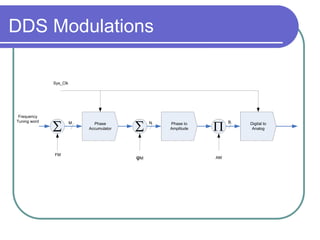

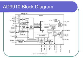
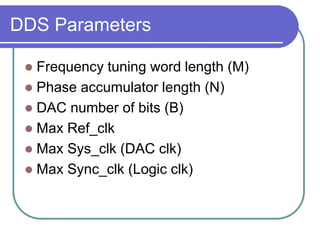
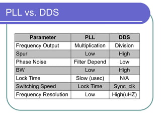
Direct digital synthesizers (DDS) generate sinusoidal waves using digital logic and a digital-to-analog converter. A DDS uses a phase accumulator, phase-to-amplitude converter, DAC and filter to produce an output waveform. Key parameters that determine the DDS output include the frequency tuning word length, phase accumulator length and DAC resolution. Compared to a PLL, a DDS has advantages like higher frequency resolution, faster switching speed and a wider bandwidth, but suffers from higher phase noise and spurs. Sources of noise and spurs in a DDS include phase truncation, DAC non-linearity, memory compression and harmonic aliasing.


![RF Module Design - [Chapter 3] Linearity](https://cdn.slidesharecdn.com/ss_thumbnails/rfch3-150613070345-lva1-app6891-thumbnail.jpg?width=640&height=640&fit=bounds)