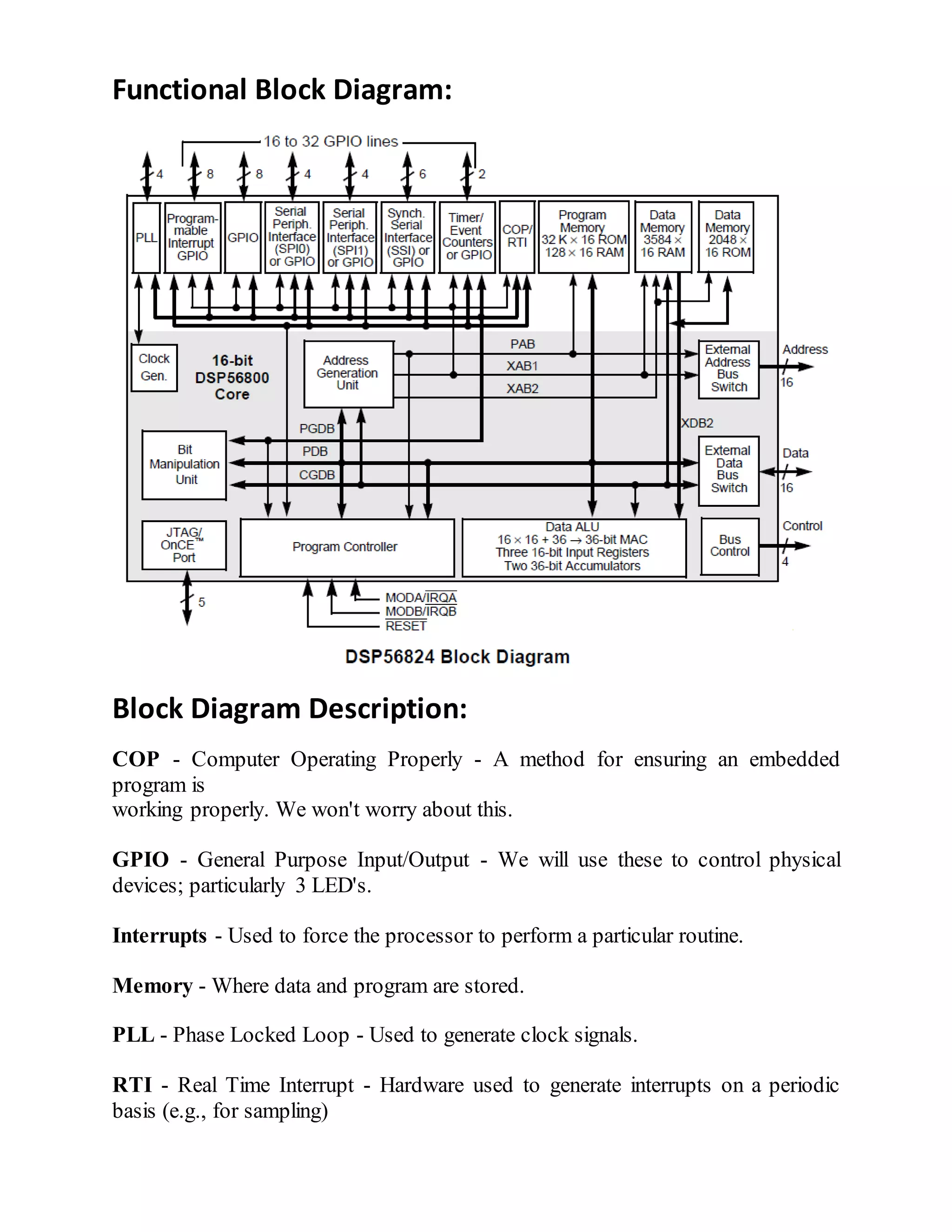
Download to read offline
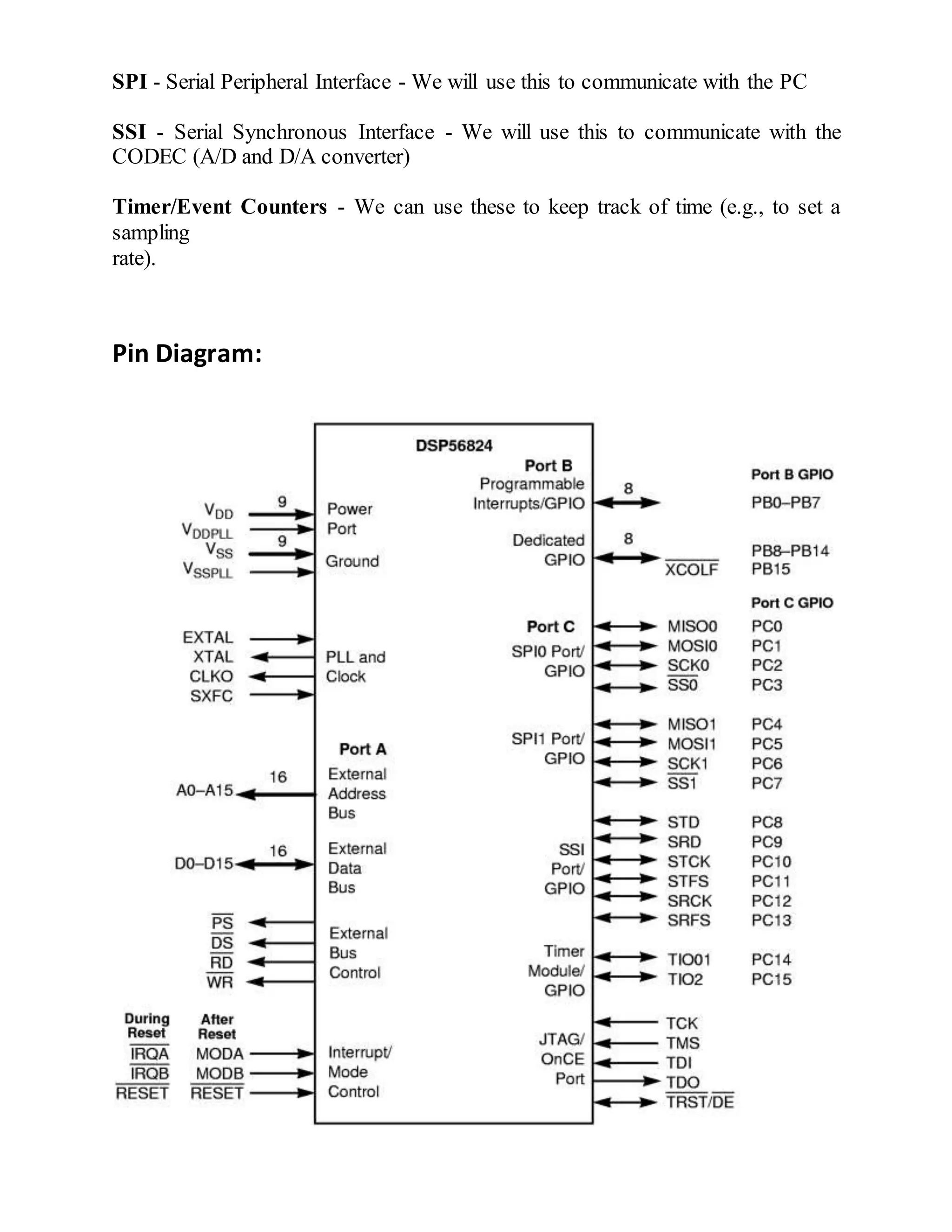
![Pin Diagram Description:
Power (VDD or VDDPLL):
VDD: These pins provide power to the internal structures of the chip, and
should all be attached to VDD.
VDDPLL: This pin supplies a quiet power source to the VCO to provide
greater frequency stability.
Ground (VSS or VSSPLL):
VSS: These pins provide grounding for the internal structures of the chip,
and should all be attached to VSS
VSSPLL: This pin supplies a quiet ground to the VCO to provide greater
frequency stability.
PLL and Clock Signals
EXTAL:
External Clock/Crystal Input—This input should be connected to an
external clock or oscillator. After being squared, the input clock can be
selected to provide the clock directly to the DSP core. The minimum
instruction time is two input clock periods, broken up into four phases
named T0, T1, T2, and T3. This input clock can also be selected as input
clock for the on-chip PLL.
XTAL:
Crystal Output—This output connects the internal crystal oscillator output to
an external crystal. If an external clock is used, XTAL should not be
connected.
CLKO
Chip- Clock Output—This pin outputs a buffered clock signal. By
programming CS[1:0] bits in the PLL Control Register(PCR1), the user can
selectbetween outputting a squared version of the signal applied to EXTAL
and a version of the DSP master clock at the output of the PLL. The clock
frequencyon this pin can also be disabled by programming the CS[1:0] bits
in PCR1](https://image.slidesharecdn.com/tae3dspprocessorashish30andakash26-160726143432/75/Study-of-Data-sheet-of-56824-DSP-processors-5-2048.jpg)
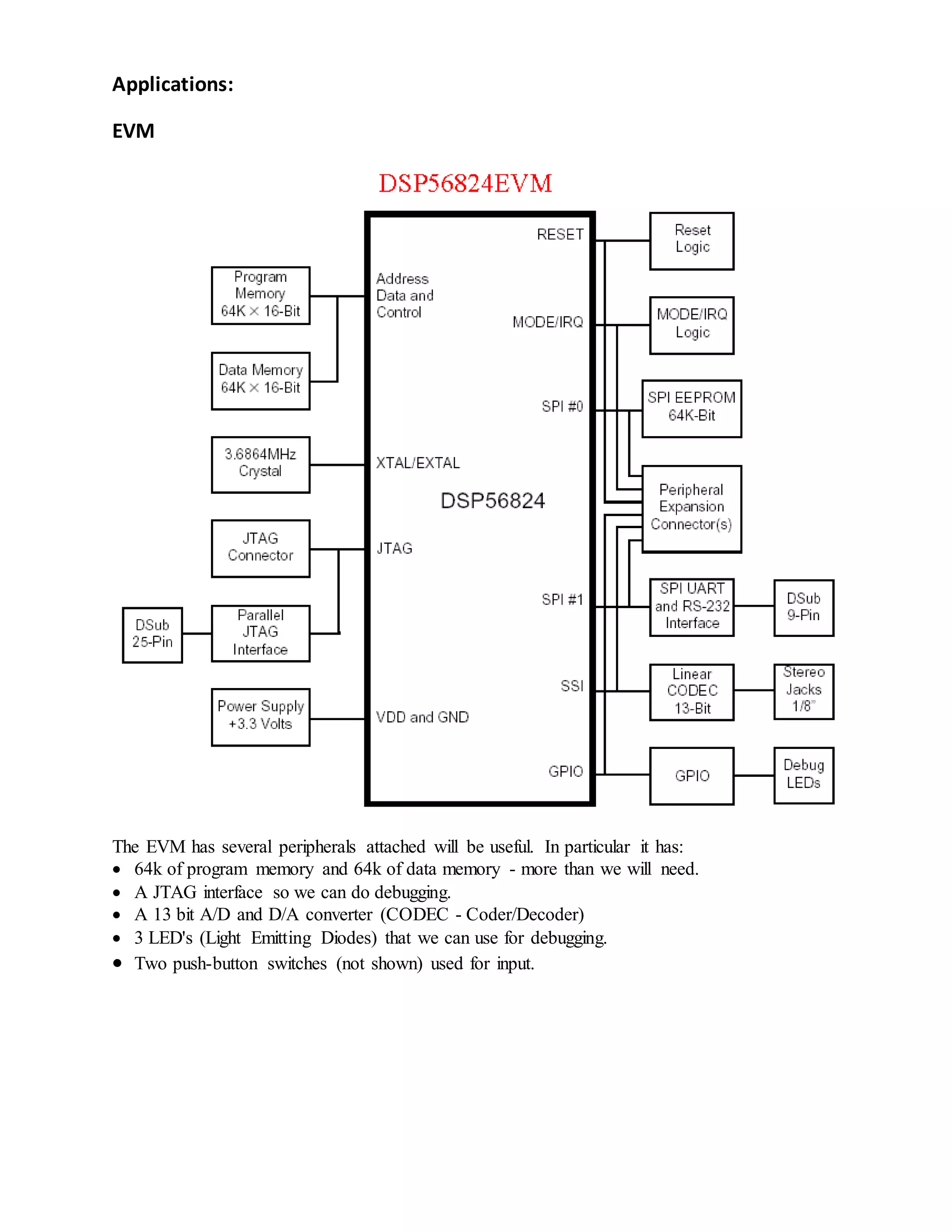

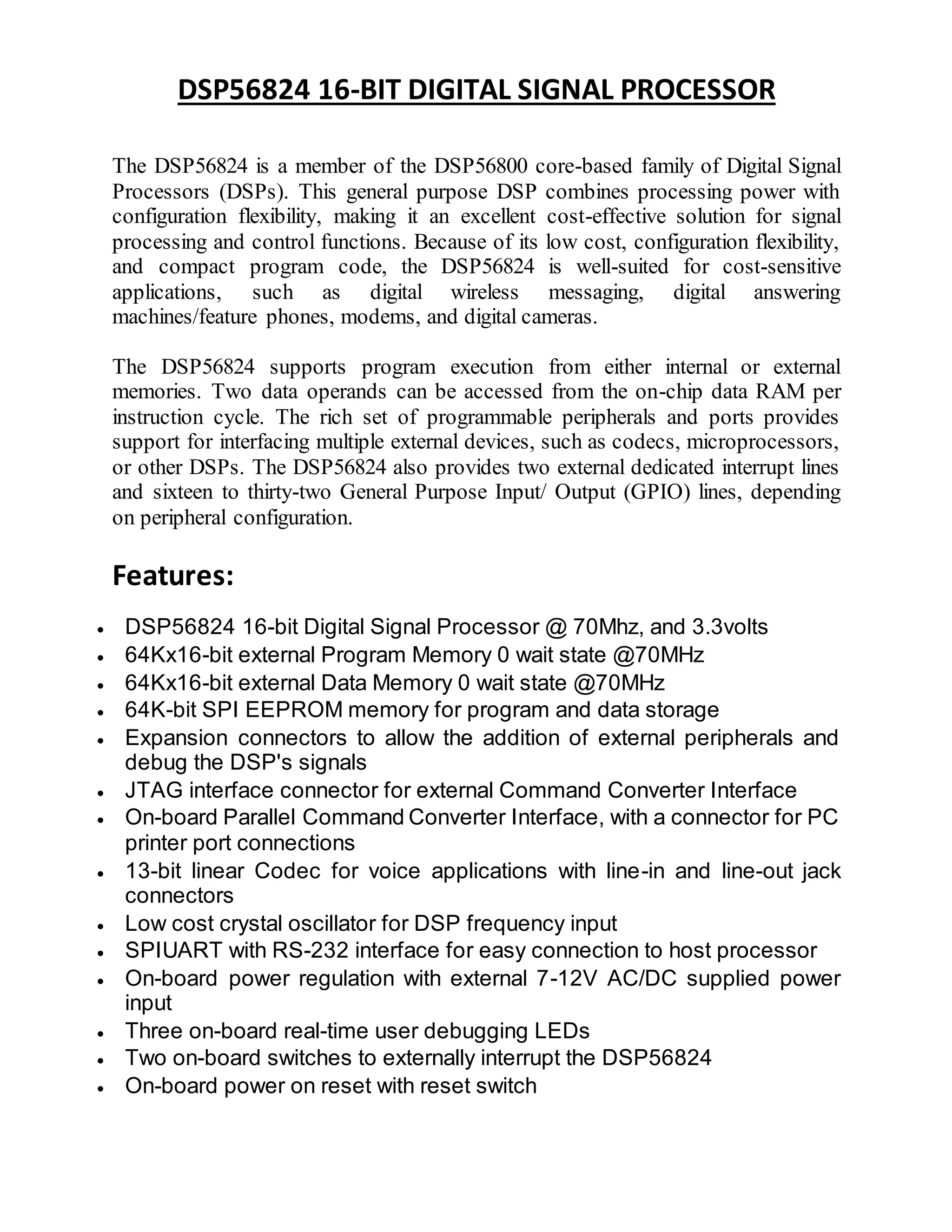
The document describes the features and specifications of the DSP56824 16-bit digital signal processor, including its programmable peripherals, memory capabilities, and interface options. It is well-suited for cost-sensitive applications like digital wireless devices and cameras due to its low cost, configuration flexibility, and compact code. The evaluation module provides peripherals like memory, a codec, LEDs, and buttons to help develop and test applications for the DSP56824.