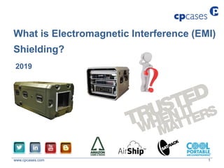
What is Electromagnetic Interference (EMI) Shielding? How to reduce EMI Shielding in cases and racks. The ERack from CP Cases is a lightweight robust rack case. Transporting mission-critical, fragile and heavy rack equipment made easier.
ITO (indium tin Oxide) & FTO (fluorine doped tin oxide )Preeti Choudhary
Indium tin oxide (ITO) is a transparent conducting oxide used in applications such as touchscreens and solar cells. It is deposited as a thin film using methods like thermal evaporation or sputtering. ITO has high electrical conductivity and optical transparency due to its large band gap. It is studied using techniques like Kelvin probe force microscopy that measure electrical properties at the nanoscale. While ITO enables important technologies, its production requires significant energy and indium is a scarce resource.
This document discusses organic transistor technology, comparing organic and inorganic semiconductors. Organic electronics are lighter, more flexible, and lower-cost to produce than silicon-based electronics. They can be fabricated at ambient temperatures using printing techniques rather than expensive cleanrooms. Key applications include displays, solar cells, and thin-film transistors. Materials mentioned include PEDOT:PSS, encapsulation epoxy, glass/plastic substrates, and a Dimatix printer for deposition of organic layers.
Photonic materials manipulate photons to achieve certain functions. Photonic crystals are a type of photonic material that displays unusual properties in interacting with light due to a periodic modulation of refractive index. They can trap light in cavities and waveguides by creating photonic band gaps that prevent light from propagating in certain directions. Potential applications of photonic crystals include photonic integrated circuits, lasers, sensors, and replacing conventional optical fibers.
Graphene is a two-dimensional sheet of carbon atoms arranged in a honeycomb lattice. Andre Geim and Konstantin Novoselov won the Nobel Prize in 2010 for their work on graphene. Graphene has many useful properties for sensors, including a large surface area, high electrical conductivity, and high mechanical strength. For graphene to function as a sensor, it often needs to be functionalized with recognition elements through covalent or non-covalent bonding to detect targets and transduce signals. Graphene can be used to create electrochemical, optical, and nanopore sensors for applications like glucose detection and biomolecular sensing.
If you have any questions, contact me. I would be happy to help.
PLEASE LIKE IT AND GIVE COMMENT
In this presentation,
The author gives the working principle of the PVD and Sputtering methods. But you can also find an information about the thin film and plasma phase of a matter.
Also this is related with Magnetron Sputtering method.
An OLED (organic light-emitting diode) is a thin film light source that emits light when an electric current is applied. OLEDs are made up of organic layers sandwiched between an anode and cathode. When voltage is applied, electrons from the cathode recombine with electron holes from the anode in the emissive organic layer, releasing energy in the form of photons. OLEDs are thinner, more efficient, and provide better contrast than LCDs. There are different types including passive-matrix, active-matrix, transparent, and flexible OLEDs. OLEDs have advantages like lower costs potential, lightweight flexible designs, and better power efficiency compared to other display technologies, but also have
TRANSPARENT ELECTRONICS
Abstract: Transparent electronics is an emerging science and technology field focused on producing ‘invisible’ electronic circuitry and opto-electronic devices.
Applications include consumer electronics, new energy sources, and transportation; for example, automobilewindshields could transmit visual information to the driver. Glass in almost any setting could also double as an electronic device, possibly improving security systems or offering transparent displays. In a similar vein, windows could be used to produce electrical power. Other civilian and military applications in this research field include realtime wearable displays.
As for conventional Si/III–V-based electronics, the basic device structure is based on semiconductor junctions and transistors. However, the device building block materials, the semiconductor, the electric contacts, and the ielectric/passivation layers, must now be transparent in the visible –a true challenge! Therefore, the first scientific goal of this technology must be to discover,understand, and implement transparent high-performance electronic materials. The second goal is their implementation and evaluation in transistor and circuit structures.
The electronics during the past 10 years, the classes of materials available for transparent electronics applications have grown dramatically. Historically, this area was dominated by transparent conducting oxides (oxide materials that are both electrically conductive and optically transparent) because of their wide use in antistatic coatings, touch display panels, solar cells, flat panel displays, heaters, defrosters, ‘smart windows’ and optical coatings. All these applications use transparent conductive oxides as passive electrical or optical coatings. The field of transparent conducting oxide (TCO) materials has been reviewed and many treatises on the topic are available. However, more recently there have been tremendous efforts to develop new active materials for functional transparent electronics. These new technologies will require new materials sets, in addition to the TCO component, including conducting, dielectric and semiconducting materials, as well as passive components for full device fabrication.
COMBINING OPTICAL TRANSPARENCY WITH ELECTRICAL CONDUCTIVITY
Transparent conductors are neither 100% optically transparent nor metallically conductive. From the band structure point of view, the combination of the two properties in the same material is contradictory: a transparent material is an insulator which possesses completely filled valence and empty conduction bands; whereas metallic conductivity appears when the Fermi level lies within a band with a large density of states to provide high carrier concentration. Efficient transparent conductors find their niche in a compromise between a sufficient transmission within the visible spectral range and a moderate but useful in practice electrical conductivity.
OLED - Organic Light Emitting Diode
Today's most rapidly growing technology in World
All display technology now change to OLED
Less Power consumption
Cost Effective
Flexible
Environment Friendly
This is a power point presentation of project work on preparing Zinc oxide thin films by using SILAR technique and CBD technique and studying its characteristics.
Perovskites-based Solar Cells: The challenge of material choice for p-i-n per...Akinola Oyedele
Perovskite-based PV have triggered widespread interest in the scientific community because these materials offer the attractive combinations of low cost and theoretically high efficiency. However, several challenges must be overcome for these relatively new PV materials. Among the many important challenges, one is the choice of materials to be used in thin film PV devices..
Based on fundamental principles of solar photovoltaics, this problem focuses on two aspects of the perovskite system:
1) Based on a planar p-i-n device structure, a potential list of p- and n-type charge collecting layers as well as the conductive contacts that could be used with a promising perovskite absorber material was identified, and a proper justification for the selection of each material in the device was given.
2) Three theoretical p-i-n type solar cells were made with the chosen materials and appropriate conductive contacts.
Graphene is a single-atom thick layer of carbon that was discovered in 2004. It has unique electrical, mechanical, and optical properties including high electron mobility, strength stronger than diamond but flexible like rubber, and ability to transmit light. These properties make it promising for applications in electronics, composites, energy storage, and more. Graphene is still in early stages of research and development.
Bismuth ferrite is a multiferroic material with rhombohedral crystal structure and Curie and Neel temperatures of 825°C and 360°C respectively. It exhibits ferroelectricity and ferromagnetism simultaneously. Bismuth ferrite nanoparticles were synthesized using a sol-gel method, which is a bottom-up approach involving hydrolysis and condensation of bismuth nitrate, iron nitrate, and citric acid precursors. The nanoparticles were characterized using X-ray diffraction, which confirmed the hexagonal crystal structure and an average crystalline size of 33.87 nm. Nanoparticle-based technologies are important for developing advanced applications in areas such as memory devices, telecommunications, and
This document provides an overview of organic electronic materials, including their properties, applications, and key developments. It discusses how charge transfer complexes and conductive polymers can have conducting, semiconducting, and light emitting properties. Important applications mentioned include organic field effect transistors, RFID tags, and OLED displays. The development of conductive polymers like polyacetylene in the 1970s led to the discovery of organic superconductors and earned several scientists the 2000 Nobel Prize in Chemistry. Flexible OLEDs and organic thin film transistors now allow for printed electronic technologies.
This document discusses multiferoic materials, which exhibit more than one "primary ferroic order parameter" simultaneously. The four primary ferroic order parameters are ferromagnetism, ferroelectricity, ferroelasticity, and antiferromagnetism/ferrimagnetism. The document provides examples of natural and synthetic multiferoic materials and discusses their properties and applications. It also explains related effects like magnetoelectricity and piezoelectricity, describing how certain materials can generate an electric potential or mechanical strain in response to a magnetic or electric field.
This document discusses electroluminescence and electroluminescent displays. It begins by defining electroluminescence as the emission of light from a material in response to electricity. There are two mechanisms for electroluminescence - intrinsic and charge injection. It then covers electroluminescent materials and devices, describing common inorganic and organic materials used, as well as the basic structure and functioning of electroluminescent displays and their advantages over other display technologies. It concludes by discussing the history and applications of electroluminescent displays.
Synthesis and properties of PolyanilineAwad Albalwi
This document summarizes the synthesis and properties of polyaniline. Polyaniline was prepared through chemical and electrochemical polymerization in acidic medium. Different solvents, including DMF and m-cresol, were compared for their effect on polyaniline's conductivity. UV-vis spectroscopy and cyclic voltammetry were used to analyze the polymer films. The conductivity of polyaniline was influenced by acidity and the electronic structure of different solvents, which impacts the polymer chain conformation. Polyaniline in m-cresol had higher conductivity than in DMF due to stronger interactions between adjacent polarons.
Perovskite: introduction, classification, structure of perovskite, method to synthesis, characterization by XRD and UV- vis spectroscopy , lambert beer's law, material properties and advantage and application.
Sensors are needed convert real life quantities into
signal variations and hence has a very high importance. Or-ganics semiconductors have their own advantages, which can
be exploited to create sensors. One of the mostly used sensor
based on organic materials is the Organic Field-Effect Transistor
(OFET). The channel material made from the organic compound
interacts with the analyte and in turn causes variations in the
device parameters.
The major applications of OFET sensors are as bio-sensors,
chemical, and gas sensors. Bio-sensors helps in disease diagnostics
by detecting DNA, proteins, enzymes etc. Chemical sensors are
used to find out the presence of ions, humidity, and pH levels. To
get more information, furthur discussion is about a single OFET
sensor fabricated with P3HT and CuTPP used for detecting nitro-based explosive compounds. OFET sensors are very promising
and could be used in real applications in near future.
A perovskite solar cell is a type of solar cell which includes a perovskite structured compound, most commonly a hybrid organic-inorganic lead or tin halide-based material, as the light-harvesting active layer.
The document introduces light emitting polymers (LEPs), which emit light when voltage is applied. It discusses the history and development of LEPs, from initial experiments in the 1950s to their invention in 1990. The document explains the basic structure of an LEP, which consists of a semiconducting polymer film sandwiched between an anode and cathode. When voltage is applied, electrons and holes migrate and combine to form excitons that emit radiation. Manufacturing techniques like spin coating and printing are also introduced. Advantages of LEPs over other displays are provided, along with some limitations and potential applications.
This document provides an overview of thin film deposition methods and thin film characterization techniques. It discusses the objectives of the course, which are to provide an understanding of thin film deposition methods, their capabilities and limitations. Hands-on demonstrations and experiments will help participants understand each deposition method and stimulate discussion. The document then summarizes various thin film deposition techniques like evaporation, sputtering, chemical vapor deposition, their principles and examples of applications. It also summarizes various characterization techniques used to analyze thin films and determine properties like composition, structure, thickness and defects.
Chemical and electrochem method of synthesis of polyaniline and polythiophene...Mugilan Narayanasamy
This document summarizes chemical and electrochemical methods for synthesizing polyaniline and polythiophene. Polyaniline can exist in three oxidation states - leucoemeraldine, emeraldine, and pernigraniline. It can be synthesized chemically using an oxidative process with an acid and oxidizing agent like ammonium persulfate or potassium dichromate. Electrochemical synthesis grows a polyaniline film on an anode. Polythiophene is also synthesized chemically using oxidative polymerization with catalysts or electrochemically by applying a potential to drive polymerization. The McCullough and Rieke methods can produce regioregular polythiophene using nickel or palladium catalysts. Both polymers find applications in
The document discusses the optical properties of materials and their applications. It begins by defining optical materials as substances that manipulate light flow and describes their interactions with electromagnetic radiation. It then covers classification of materials as transparent, translucent, or opaque based on light transmission. Specific optical properties like reflection, refraction, absorption, and transmission are defined. Applications such as luminescence, lasers, photoconductivity, and optical fibers are also summarized.
Fabrication and characterization of bismuth ferrite nanofiber by electrospinn...Abthul Hakkeem
This document summarizes a thesis on fabricating and characterizing bismuth ferrite nanofibers using electrospinning. Bismuth ferrite is a multiferroic material with applications in transducers, sensors, and memory. Nanofibers were produced at varying voltages and characterized. X-ray diffraction showed the 10 kV fibers were phase pure while others contained impurities. Scanning electron microscopy found the 10 and 15 kV fibers had the best morphology and size distribution. The thesis evaluated how the applied voltage impacts fiber properties.
Organic electronics is a branch of electronics dealing with conductive polymers and small molecules. Conductive polymers are lighter, more flexible, and less expensive than inorganic conductors, making them desirable for many applications. Significant developments include the discovery that doping polyacetylene with iodine increases its conductivity by 12 orders of magnitude, and the invention of the organic light-emitting diode and organic photovoltaic cell. Organic electronics utilize carbon-based materials and offer advantages over traditional silicon-based electronics such as lower cost, mechanical flexibility, and lower processing temperatures.
X-Ray Photoelectron Spectroscopy (XPS) is a surface-sensitive technique that uses X-rays to eject electrons from a material's surface and measure their kinetic energy. An XPS instrument subjects a sample to a monoenergetic X-ray beam in an ultra-high vacuum, which ejects core-level electrons. A cylindrical mirror analyzer measures the electrons' kinetic energies, allowing their binding energies to be calculated and identifying the elemental composition of the top 1-10 nanometers of the sample surface. XPS provides both qualitative and quantitative analysis of elements present on the surface and can be used to study polymers, catalysts, corrosion, thin films and more.
Instrumentation Cable In India are a couple of conductor cables that carry low strength electric indicators used for tracking or controlling electric strength structures and their related approaches.
The ever-increasing use of high-frequency switching devices in industrial automation can result in high-frequency currents circulating in an equipotential bonding network that was not designed for this purpose. The absence of a proven low-impedance bonding network can result in these currents taking alternative and often undesirable routes. Occasionally these will be the shields of industrial network cables such as PROFIBUS and PROFINET that in turn can lead to intermittent communications problems. This presentation will discuss the issues in more detail and will explain the relevance of the recently released PI guidelines “Functional Bonding and Shielding for PROFIBUS and PROFINET”.
1. EMI problems in industrial networks are often caused by power electronics like variable frequency drives. Proper cable shielding and grounding can help mitigate these issues.
2. PROFIBUS and PROFINET networks are designed to operate in industrial environments using screened twisted pair cable for protection against electrostatic and electromagnetic interference. Connecting cable shields to a common reference at both ends is important.
3. A meshed grounding network provides the lowest impedance reference for cable shields and is recommended for effective EMC grounding. Disconnecting cable shields can cause communication problems and should be avoided.
Hybrid battery +solar pv grid tie power project presentation by jmv lpsMahesh Chandra Manav
JMV provides electrical safety equipment including earthing and lightning protection systems. A presentation covered best practices for electrical equipment installation and safety, including earthing design and lightning protection standards. Earthing is critical for safety and must follow standards to be below certain ohm levels. Lightning can cause fires, so proper protection like early streamer emission air terminals that protect an area of 120 meters are recommended. JMV offers clients surge protection, earthing materials, and expertise in lightning risk assessment to protect lives and property from electrical hazards.
ARDUINO MICROCONTROLLER BASED UNDERGROUND CABLE FAULT DISTANCE LOCATORIAEME Publication
1. The document describes an Arduino microcontroller-based device for locating faults in underground cable lines. It uses basic Ohm's law to detect faults by measuring variations in current with respect to resistance at different points along the cable.
2. The device has several units - a power supply, cable unit with switches to induce faults, control unit to process signals from the cable unit, tripping unit to detect faulty phases, and a display unit to show fault characteristics and distance on an LCD screen.
3. Common underground cable faults include short circuits, open circuits, and earth faults between phases and ground, which can be caused by insulation damage, loose connections, and other factors related to aging of cable materials over time
Fertilizer and Chemical Process Plant ,Food and Pharma , PDIL,EIL,Development Consultant India Pvt Ltd Tata Consulting Engineers;MECON;HURL,PLC and DCS Manufacturer /System Intergrators/EPC Companies Handling Electrical and C&I Projects.
Electrical wiring is the installation of cabling and devices like switches and sockets within a structure. Proper wiring is important for safety and must follow standards for design, materials, and installation. Wiring codes vary by location but aim to harmonize standards globally. Modern wiring uses plastic-coated cables in various configurations depending on the voltage and environment. Special cable types are used in industrial settings and marine applications due to demanding conditions.
Prysmian manufactures composite screened cables for use in underground coal mines. The Type 209 cable is designed for general use in underground mines from 1.1-11kV in accordance with Australian standards. It has tinned copper conductors, EPR insulation, a composite screen, and a heavy duty PCP sheath. The cable is highly flexible and resistant to harsh and wet underground mining environments.
This document provides an overview of Carlisle Interconnect Technologies' locations and product offerings. It lists various locations and contact people around the world, describing what each location focuses on in terms of manufacturing and products. It then summarizes some of Carlisle's key product lines, including contacts and connectors, RF and microwave cables, optical cables, wire and cable, power and grounding products, and integrated systems. The document emphasizes Carlisle's vertical integration and capabilities across the supply chain. It provides high-level descriptions of products and manufacturing processes to give the reader a sense of Carlisle's broad range of capabilities in the interconnect industry.
The document discusses lightning protection standards and earthing design requirements. It recommends the following earthing designs:
- For large substations, earthing resistance should be below 1 ohm.
- For small substations and telecom/SCADA systems, earthing resistance should be below 0.5-2 ohms.
- Tower and other structures should have 8-15 ohm earthing.
- Lightning protection systems require 5 ohm or less for 50kA strikes and 8-15 ohms for 100kA strikes.
- Exothermic welding and hybrid metal rods are recommended for connections.
UAV cable, Tethered drone Cable
We strike a balance by blending power and fiber optic cables with rugged materials in a small-scale hybrid design. Our tethered drone cables are 20% smaller than standard cables built with nylon, so they take up less space inside the Tether Management System (TMS), which means more design options and extra payload during operation.
1. The document lists 10 common NEC violations seen in low voltage systems installations. These include running audio cables with other low voltage cables, power cords above ceilings, cables suspended from cable trays without additional supports, unlisted coaxial cables run inside buildings over 50 feet, improper use of primary and secondary protectors, patch cords in plenum spaces, low voltage cables run with non-class 2 power supplies, ungrounded or improperly grounded protectors, unlisted communication cables in EMT conduit over 50 feet, and insulated grounding cables in air handling spaces.
2. Inspectors often miss low voltage code violations as their focus is on major electrical systems and low voltage work may not be complete during ins
Power transmission and distribution along with power qualty presentation by j...Mahesh Chandra Manav
All Electrical Contractor Power T&D Substation/eBOPContractor Power T&D Substation/CPWD/PWD/Smart Cities/Project AMRUT/Central and State Power T&D Substation Departments
Phelps Dodge International (Thailand) Limited is a leading manufacturer of medium and high voltage power cables. It has state-of-the-art facilities in Thailand that can produce cables rated up to 245kV. The company uses high quality materials and stringent quality control processes to ensure reliable cables that meet international standards. It has extensive experience in manufacturing cables for power distribution systems.
Change rooms and anterooms play vital roles in maintaining hygiene and safety standards within the food industry. Change rooms provide designated areas for employees to change into clean garments before entering production areas, while anterooms serve as transitional spaces, minimizing the risk of contaminants entering sterile zones. These facilities are essential for preventing cross-contamination and upholding strict quality control measures in food processing environments.
Cables are essential components of modern technology, facilitating the transmission of data, power, and signals across various industries. They come in different types, including fiber optic, coaxial, twisted pair, and Ethernet cables, each designed for specific applications.
Stay Ahead of the Curve with Our Weekly Food-Tech Insights: Your Gateway to the Latest Innovations, Trends, and Industry buzz!
See the latest presentation from CP Cases - Military standard protective cases and 19" equipment rack mount cases for air transport, weapons cases, satellite communications, medical equipment and more. All cases are field ready for extreme weather conditions and have been designed to be robust and secure for storage, transport and field operations.
Building perfect defence quality aerospace wire harnesses requires critical considerations. This is why you should partner with a reputed defence wire harness manufacturer in India.
Similar to CP Cases - What is electromagnetic shielding? (20)
A SYSTEMATIC RISK ASSESSMENT APPROACH FOR SECURING THE SMART IRRIGATION SYSTEMSIJNSA Journal
The smart irrigation system represents an innovative approach to optimize water usage in agricultural and landscaping practices. The integration of cutting-edge technologies, including sensors, actuators, and data analysis, empowers this system to provide accurate monitoring and control of irrigation processes by leveraging real-time environmental conditions. The main objective of a smart irrigation system is to optimize water efficiency, minimize expenses, and foster the adoption of sustainable water management methods. This paper conducts a systematic risk assessment by exploring the key components/assets and their functionalities in the smart irrigation system. The crucial role of sensors in gathering data on soil moisture, weather patterns, and plant well-being is emphasized in this system. These sensors enable intelligent decision-making in irrigation scheduling and water distribution, leading to enhanced water efficiency and sustainable water management practices. Actuators enable automated control of irrigation devices, ensuring precise and targeted water delivery to plants. Additionally, the paper addresses the potential threat and vulnerabilities associated with smart irrigation systems. It discusses limitations of the system, such as power constraints and computational capabilities, and calculates the potential security risks. The paper suggests possible risk treatment methods for effective secure system operation. In conclusion, the paper emphasizes the significant benefits of implementing smart irrigation systems, including improved water conservation, increased crop yield, and reduced environmental impact. Additionally, based on the security analysis conducted, the paper recommends the implementation of countermeasures and security approaches to address vulnerabilities and ensure the integrity and reliability of the system. By incorporating these measures, smart irrigation technology can revolutionize water management practices in agriculture, promoting sustainability, resource efficiency, and safeguarding against potential security threats.
Presentation of IEEE Slovenia CIS (Computational Intelligence Society) Chapte...University of Maribor
Slides from talk presenting:
Aleš Zamuda: Presentation of IEEE Slovenia CIS (Computational Intelligence Society) Chapter and Networking.
Presentation at IcETRAN 2024 session:
"Inter-Society Networking Panel GRSS/MTT-S/CIS
Panel Session: Promoting Connection and Cooperation"
IEEE Slovenia GRSS
IEEE Serbia and Montenegro MTT-S
IEEE Slovenia CIS
11TH INTERNATIONAL CONFERENCE ON ELECTRICAL, ELECTRONIC AND COMPUTING ENGINEERING
3-6 June 2024, Niš, Serbia
Embedded machine learning-based road conditions and driving behavior monitoringIJECEIAES
Car accident rates have increased in recent years, resulting in losses in human lives, properties, and other financial costs. An embedded machine learning-based system is developed to address this critical issue. The system can monitor road conditions, detect driving patterns, and identify aggressive driving behaviors. The system is based on neural networks trained on a comprehensive dataset of driving events, driving styles, and road conditions. The system effectively detects potential risks and helps mitigate the frequency and impact of accidents. The primary goal is to ensure the safety of drivers and vehicles. Collecting data involved gathering information on three key road events: normal street and normal drive, speed bumps, circular yellow speed bumps, and three aggressive driving actions: sudden start, sudden stop, and sudden entry. The gathered data is processed and analyzed using a machine learning system designed for limited power and memory devices. The developed system resulted in 91.9% accuracy, 93.6% precision, and 92% recall. The achieved inference time on an Arduino Nano 33 BLE Sense with a 32-bit CPU running at 64 MHz is 34 ms and requires 2.6 kB peak RAM and 139.9 kB program flash memory, making it suitable for resource-constrained embedded systems.
A review on techniques and modelling methodologies used for checking electrom...nooriasukmaningtyas
The proper function of the integrated circuit (IC) in an inhibiting electromagnetic environment has always been a serious concern throughout the decades of revolution in the world of electronics, from disjunct devices to today’s integrated circuit technology, where billions of transistors are combined on a single chip. The automotive industry and smart vehicles in particular, are confronting design issues such as being prone to electromagnetic interference (EMI). Electronic control devices calculate incorrect outputs because of EMI and sensors give misleading values which can prove fatal in case of automotives. In this paper, the authors have non exhaustively tried to review research work concerned with the investigation of EMI in ICs and prediction of this EMI using various modelling methodologies and measurement setups.
Electric vehicle and photovoltaic advanced roles in enhancing the financial p...IJECEIAES
Climate change's impact on the planet forced the United Nations and governments to promote green energies and electric transportation. The deployments of photovoltaic (PV) and electric vehicle (EV) systems gained stronger momentum due to their numerous advantages over fossil fuel types. The advantages go beyond sustainability to reach financial support and stability. The work in this paper introduces the hybrid system between PV and EV to support industrial and commercial plants. This paper covers the theoretical framework of the proposed hybrid system including the required equation to complete the cost analysis when PV and EV are present. In addition, the proposed design diagram which sets the priorities and requirements of the system is presented. The proposed approach allows setup to advance their power stability, especially during power outages. The presented information supports researchers and plant owners to complete the necessary analysis while promoting the deployment of clean energy. The result of a case study that represents a dairy milk farmer supports the theoretical works and highlights its advanced benefits to existing plants. The short return on investment of the proposed approach supports the paper's novelty approach for the sustainable electrical system. In addition, the proposed system allows for an isolated power setup without the need for a transmission line which enhances the safety of the electrical network
Advanced control scheme of doubly fed induction generator for wind turbine us...IJECEIAES
This paper describes a speed control device for generating electrical energy on an electricity network based on the doubly fed induction generator (DFIG) used for wind power conversion systems. At first, a double-fed induction generator model was constructed. A control law is formulated to govern the flow of energy between the stator of a DFIG and the energy network using three types of controllers: proportional integral (PI), sliding mode controller (SMC) and second order sliding mode controller (SOSMC). Their different results in terms of power reference tracking, reaction to unexpected speed fluctuations, sensitivity to perturbations, and resilience against machine parameter alterations are compared. MATLAB/Simulink was used to conduct the simulations for the preceding study. Multiple simulations have shown very satisfying results, and the investigations demonstrate the efficacy and power-enhancing capabilities of the suggested control system.
Literature Review Basics and Understanding Reference Management.pptxDr Ramhari Poudyal
Three-day training on academic research focuses on analytical tools at United Technical College, supported by the University Grant Commission, Nepal. 24-26 May 2024
Understanding Inductive Bias in Machine LearningSUTEJAS
This presentation explores the concept of inductive bias in machine learning. It explains how algorithms come with built-in assumptions and preferences that guide the learning process. You'll learn about the different types of inductive bias and how they can impact the performance and generalizability of machine learning models.
The presentation also covers the positive and negative aspects of inductive bias, along with strategies for mitigating potential drawbacks. We'll explore examples of how bias manifests in algorithms like neural networks and decision trees.
By understanding inductive bias, you can gain valuable insights into how machine learning models work and make informed decisions when building and deploying them.
2. www.cpcases.com 2
EMI and EMI Shielding?
EMI?
Electromagnetic Interference (EMI) is the adverse effect of electromagnetic
fields on other devices. The interference is produced as the fluctuating field
traverses’ other devices or their connecting cables or PCB tracks. Each
traverse induces a voltage which may be quite small. However, data
processing devices run on low voltages and these induced voltages are
relatively large and can easily corrupt input and output data signals.
Environmental electromagnetic conditions are, by their nature, unpredictable
so shielding is designed to remove this performance threat.
EMI Shielding?
It is a form of insulation / conductive barrier that reduces or prevents transfer
of energy, in this case electromagnetic energy, escaping or entering a
system and interfering with other devices in the same environment. So for
example, a gentle hum from the home radio when your mobile phone rings.
3. www.cpcases.com 3
EMI shielding effectiveness
In designing a protective solution, CP Cases has worked
closely with customers to develop enclosures to effectively
shield devices. This enclosure must completely envelope the
device.
Usually there is a need to access the device and so the
enclosure will be in at least two parts. There must be
conductive continuity between these parts or else the
interference may ‘leak’ in through the gap between them.
Continuous face to face contact between a case and its lid
with the precision required is not reliable. Add in other
environmental hazards, such as dust and water, requiring
flexible seals. Flexible seals in rubber are transparent to EMI
and so must be enclosed in knitted metal wire sleeves to
contact both parts.
Some equipment requires air cooling whilst still maintaining
the shield. Holes or slots in the shield would act as aerials and
allow the EMI to re-radiate within the enclosure. Generally, if
any hole or slot is under 3mm an effective shield can be
maintained.
ERack Lightweight 19″ Ruggedised Enclosures are examples of this technology
in practice.
4. www.cpcases.com 4
Reducing EMI interference
A metal shield or screen will block EMI, especially if the barrier is
connected to ground. Audio and video cables, for example, consist
of an inner conductor surrounded by a braided outer shield; EMI
enters the shield and flows directly to ground instead of interfering
with the signals the cable is carrying. A grounded metal equipment
chassis also acts as an EMI shield for circuits inside the cabinet.
The ultimate form of EMI shield is a box called a Faraday cage.
This is a conductive enclosure that keeps voltages out because
charges repel each other sideways. Dimensions of the openings in
the cage determine what voltages will be excluded. For electronic
devices any opening must be small but do not need to be ‘airtight’.
EMI is regulated worldwide and there are standards to follow such
as those set by the FCC in the US, CE in Europe, and ICES in
Canada. This is broken into two main parts; conducted and
radiated.
CP Cases products can be designed in line with Electromagnetic
Compatibility (EMC) directives and the UK defence standard for
EMC, DEF STAN 59-41.
5. www.cpcases.com 5
EMI Best Practise Case Study
CP Cases experience with EMI was put to the
test through a project with the Aircraft Carrier
Alliance (ACA) where Rackmount Enclosures for
QE Class Aircraft Carriers were delivered.
CP Cases supplied more than 1200 custom-
designed rackmount enclosures and more than
4000 adaptors and brackets, for installation on-
board two (QE) Class aircraft carriers to house
datacoms enclosures of various sizes.
The smallest enclosure accommodates two single units of 19” rack-mounted network
switches; the largest cabinet stands almost five feet tall and can accommodate 29
units. Also developed especially for the project were a series of plinths and brackets,
which secure telephone handsets to horizontal and vertical surfaces around the ship.
Working closely with BAE Systems, one of the four Aircraft Carrier Alliance (ACA)
partners, CP also integrated the power supply wiring, voltage filter and cable
management systems to ensure the enclosures were ‘plug & play’ ready.
6. www.cpcases.com 6
About the product
The primary function of the network equipment enclosures was to provide physical and
electromagnetic security to various types of Cisco IE Ethernet network switches and the
thousands of accompanying connecting datacoms, Ethernet and fibre optic cables.
The communications requirement was substantial – the carriers need constant contact
with all in-flight aircraft, the consort group, HQ and land forces. The network switches
process and route this vital communications data.
Each enclosure protects the 19” rack mounted
switches from vibration, impact, particle and
moisture ingress, and also provide screening
from any electromagnetic interference
(EMC/EMI) that could disrupt the mission
communication systems from radar energy
and other strong electromagnetic signals
which are emanating from various positions
on board, ensuring the ship’s sensors do their
job without adversely affecting each other.
7. www.cpcases.com 7
EMC Functionality
CP Cases introduced and utilised novel designs embracing
the same materials developed specifically for EMC/EMI
screening used as part of the ‘ERACK’ series of portable
Anti- Vibration rackmount containers, which are
performance certified to provide a high level of
electromagnetic shielding.
The solution for providing electromagnetic compatibility throughout all sizes of
enclosures, also manages interference which could potentially emanate where the data
transfers cables enter and exit the enclosures. CP Cases developed a unique Cable
Entry Port (CEP) which allows cables, with accompanying connectors, to be fed into
and out of the enclosure through a simple “foam flap” letterbox system.
This specially designed (and EMI/EMC performance certified) CEP, uses conductive
closed-cell polyethylene foam, which compresses around individual data cables.
Conventionally, each cable would have been installed via an individual four part metallic
cable gland, and bearing in mind that many enclosures have up to 144 individual cable
entry & exit points, the CEP system provides significant advantages on installation
labour hours, providing substantial cost benefits and ensures any future systems
upgrades are implemented efficiently.
8. www.cpcases.com 8
Internal Functions
Cable management rails inside the enclosures
with hook-n-loop cable ties ensure that the
recommended bend radius for each data-coms
cable is never compromised and that network
switch gear connections are safe-guarded against
accidental disconnections.
In parallel with EMI/EMC security, a primary
function was to provide simplicity during
equipment installation, maintenance and cable
connectivity. Top and front covers are secured with
unique tamper-resistant TORX PLUS® fasteners
ensuring access is limited to authorised service
personnel. Ventilation panels in key areas, provide
natural convection that dissipates any heat build-
up.
The thermoplastic powder coated surface finish is
applied onto an etch primed base; pale grey, it’s
applied electrostatically without solvents and
cured with heat to provide a hard wearing semi-
gloss surface finish. This is tougher and much less
hazardous than conventional liquid paint coatings
and has exceptionally high corrosion resistance.
9. www.cpcases.com 9
Erack® Range
Designed for transporting fragile and heavy rack equipment - 30% lighter than most
other rack cases.
Accredited to MIL-STD-810F, DEF STANN 00-35, IP rating 65, RoHS compliant with
NATO stock numbers.
ERacks design is constructed from a high-tensile aluminium alloy
Suitable for heavy payloads of up to 70kg plus
Delivers exceptional strength to weight ratio
Folded rim makes the cases stronger, lighter and more dust/water resistant
Easy re-positioning of the rack chassis
Braided earth grounding strap
Font and rear access
Interchangeable lids
Climate control COOL portable air conditioning units optional
Erack Cases
10. www.cpcases.com 10
Climate Control
Solid state climate control Thermoelectric Unit (TEU)
Ideal for remote locations and extreme temperatures
Not sensitive to orientation
Long lifetime and low maintenance
Available for Amazon Racks or ERack, and as COOL-COLLAR™
or built in to rack-body .
Available in Thermoelectric or Vapour Compression Cycle formats.
Recessed, sprung handles and inboard lid latches
Stackable with inter-locating ribs on container top & bottom
surfaces
Compatible with most Amazon and ERack accessories.
Suitable for 6U to 12U height equipment.
Maintaining optimal operating conditions of electronics
12. www.cpcases.com 12
About CP Cases
CP Cases design and manufacture rugged, impact
resistant cases, containers and electronic racks
For transport, storage and operation of essential
equipment
Well equipped factories in North America & UK/Europe
Established more than 45 years
Skilled designers, engineers and craftsmen using
CAD/CAM software and manufacturing processes
Export >50 countries
5 star financial rating
13. www.cpcases.com 13
ISO 9001 - quality assured certification (since 1993)
SSE - Society of Environmental Engineers
GSA Advantage - assisting Federal employees worldwide by
meeting today's acquisition challenges
MAKEuk - The Manufacturers’ Organisation
DMA - The Defence Manufacturers Association
ADS - UK Aerospace, Defence, Security and Space sectors
WEAF - West of England Aerospace Forum
IABM - International Association of Broadcast Manufacturers
GTC - Guild of Television Camera Professionals
About CP Cases
14. www.cpcases.com 14
THANK YOU
For more information contact:
CP Cases
W: cpcases.com
E: info@cpcases.com
T: 44 (0) 208 568 1881
Follow us too!