Download to read offline


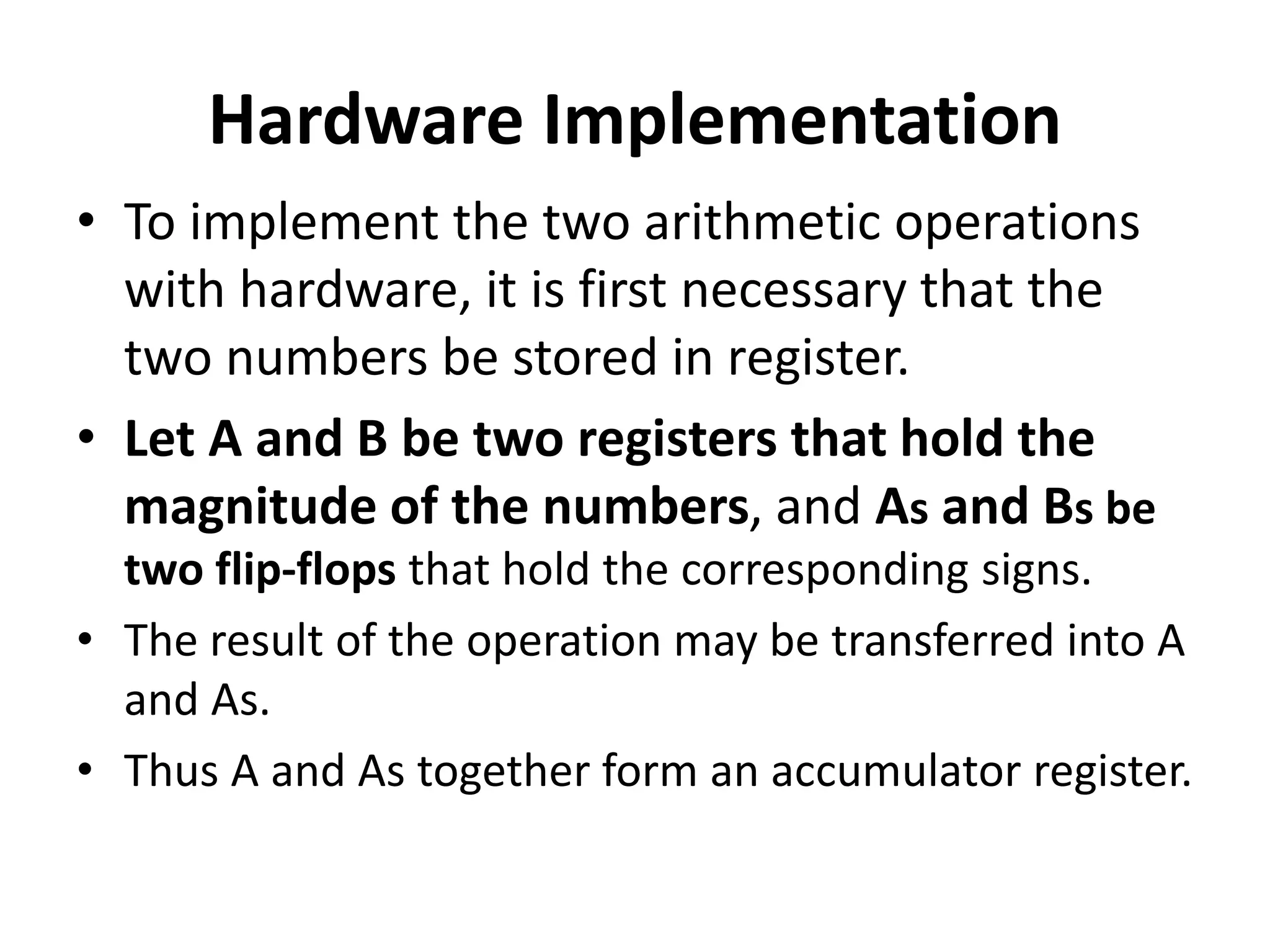


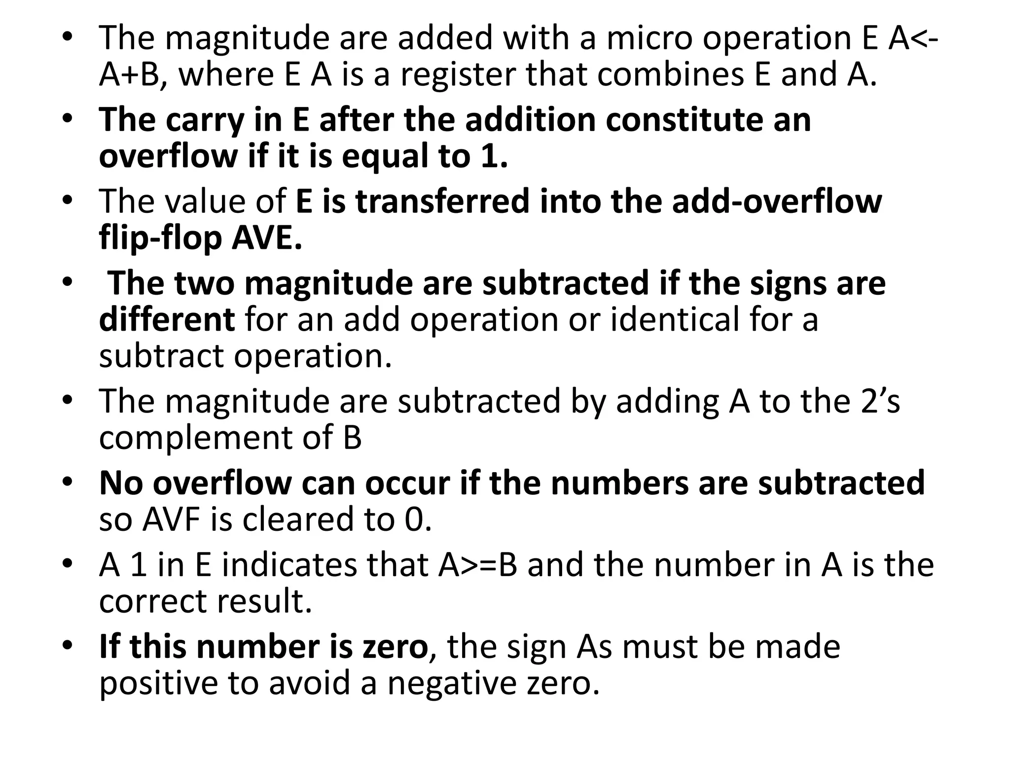
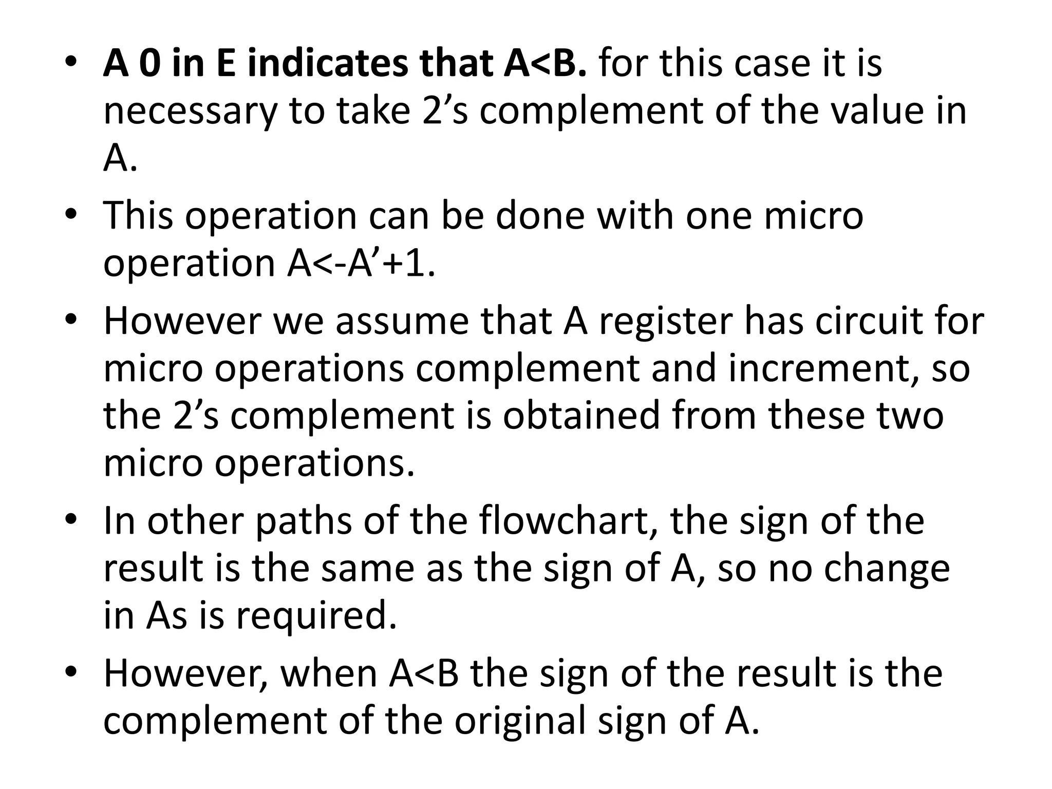


The document discusses addition, subtraction, multiplication, and division algorithms for signed binary numbers. It describes the process for each operation step-by-step including comparing sign bits, performing the operation, and determining the final result. Hardware implementations for addition/subtraction and multiplication are also covered, showing how the algorithms can be physically realized using components like registers, adders, and shift registers.