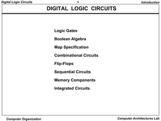
Digital Logic Circuits

1

Introduction

DIGITAL LOGIC CIRCUITS

Logic Gates
Boolean Algebra
Map Specification
Combinational Circuits
Flip-Flops
Sequential Circuits
Memory Components
Integrated Circuits

Computer Organization

Computer Architectures Lab
Digital Logic Circuits

2

Logic Gates

LOGIC GATES
Digital Computers
- Imply that the computer deals with digital information, i.e., it deals
with the information that is represented by binary digits
- Why BINARY ? instead of Decimal or other number system ?
* Consider electronic signal
7
6
5 signal
4
3 range
2
1
0

1

0
binary
*C
Consider the calculation cost - Add
id th
l l ti
t
0 1
0 0 1
1 1 10

Computer Organization

octal
0
1
2
3
4
5
6
7
8
9

0 1 2 3 4 5 6 7 8 9
0 1 2 3 4 5 6 7 8 9
1 2 3 4 5 6 7 8 9 10
2 3 4 5 6 7 8 9 1011
3 4 5 6 7 8 9 101112
4 5 6 7 8 9 10111213
5 6 7 8 9 1011121314
6 7 8 9 101112131415
7 8 9 10111213141516
8 9 1011121314151617
9 101112131415161718

Computer Architectures Lab
Digital Logic Circuits

3

Logic Gates

BASIC LOGIC BLOCK - GATE Binary
Digital
Input
Signal

.
.
.

Gate

Binary
Digital
Output
Signal

Types of Basic Logic Blocks
- Combinational Logic Block
Logic Blocks whose output logic value
depends only on the input logic values
- Sequential Logic Block
Logic Blocks whose output logic value
depends on the input values and the
state (stored information) of the blocks
Functions of Gates can be described by
- Truth Table
- Boolean Function
- Karnaugh Map
Computer Organization

Computer Architectures Lab
Digital Logic Circuits

4

Logic Gates

COMBINATIONAL GATES
Name
AND
OR

Symbol
A
B
A
B

Function
X

X

X=A•B
or
X = AB

X=A+B

I

A

X

A

X

A
0
0
1
1
A
0
0
1
1

X=A

Buffer

Truth Table

X=A

NAND

A
B

NOR
XOR

A
B
A

Exclusive OR

B

XNOR

A

Exclusive NOR
or Equivalence

B

Computer Organization

X

X = (AB)’
(AB)

X

X = (A + B)’

X

X=A⊕B
or
X = A’B + AB’

X

X = (A ⊕ B)’
or
X = A’B’+ AB

A
0
0
1
1
A
0
0
1
1
A
0
0
1
1
A
0
0
1
1

B
0
1
0
1
B
0
1
0
1

A
0
1
A
0
1
B
0
1
0
1
B
0
1
0
1
B
0
1
0
1
B
0
1
0
1

X
0
0
0
1
X
0
1
1
1
X
1
0
X
0
1
X
1
1
1
0
X
1
0
0
0
X
0
1
1
0
X
1
0
0
1

Computer Architectures Lab
Digital Logic Circuits

5

Boolean Algebra

BOOLEAN ALGEBRA
Boolean Algebra
* Algebra with Binary(Boolean) Variable and Logic Operations
g
y
y
* Boolean Algebra is useful in Analysis and Synthesis of
Digital Logic Circuits
- Input and Output signals can be
represented by Boolean Variables, and
p
y
,
- Function of the Digital Logic Circuits can be represented by
Logic Operations, i.e., Boolean Function(s)
- From a Boolean function, a logic diagram
can be constructed using AND, OR, and I
g
,
,
Truth Table
* The most e e e ta y spec cat o o t e function o a Digital Logic
e ost elementary specification of the u ct o of
g ta og c
Circuit is the Truth Table
- Table that describes the Output Values for all the combinations
of the Input Values, called MINTERMS
- n input variables → 2n minterms
Computer Organization

Computer Architectures Lab
Digital Logic Circuits

6

Boolean Algebra

LOGIC CIRCUIT DESIGN
x
0
0
0
0
1
1
1
1

Truth
Table

Boolean
Function

Logic
Diagram

Computer Organization

y
0
0
1
1
0
0
1
1

z
0
1
0
1
0
1
0
1

F
0
1
0
0
1
1
1
1

F = x + y’z

x
y

F

z
Computer Architectures Lab
Digital Logic Circuits

7

Boolean Algebra

BASIC IDENTITIES OF BOOLEAN ALGEBRA
[1] x + 0 = x
[3] x + 1 = 1
[5] x + x = x
[7] x + x’ = 1
[ ]
[9] x + y = y + x
[11] x + (y + z) = (x + y) + z
[13] x(y + z) = xy +xz
[15] (x + y)’ = x’y’
[17] (x’)’ = x

[2] x • 0 = 0
[4] x • 1 = x
[6] x • x = x
[8] x • X’ = 0
[ ] y yx
[10] xy = y
[12] x(yz) = (xy)z
[14] x + yz = (x + y)(x + z)
[16] (xy)’ = x’ + y’
[15] and [16] : De Morgan’s Theorem

Usefulness of this Table
- Simplification of the Boolean function
- Derivation of equivalent Boolean functions
to obtain logic diagrams utilizing different logic gates
tili ing
-- Ordinarily ANDs, ORs, and Inverters
-- But a certain different form of Boolean function may be convenient
to obtain circuits with NANDs or NORs
→ A li ti
Applications of De Morgans Theorem
fD M
Th
x’y’ = (x + y)’
I, AND → NOR

Computer Organization

x’+ y’= (xy)’
I, OR → NAND

Computer Architectures Lab
Digital Logic Circuits

8

Boolean Algebra

EQUIVALENT CIRCUITS
Many different logic diagrams are possible for a given Function
F = ABC + ABC’ + A’C
= AB(C + C’) + A’C
C) AC
= AB • 1 + A’C
= AB + A’C
(1)

.......…… (1)
[13] ..…. (2)
[7]
[4] ...…. (3)

A
B
C
F

(2)

A
B
F

C

(3)

A
B

F

C

Computer Organization

Computer Architectures Lab
Digital Logic Circuits

9

Boolean Algebra

COMPLEMENT OF FUNCTIONS
A Boolean function of a digital logic circuit is represented by only using
logical variables and AND, OR, and Invert operators.
→ Complement of a Boolean function
- Replace all the variables and subexpressions in the parentheses
appearing in the function expression with their respective complements
A,B,...,Z,a,b,...,z
A B Z a b z ⇒ A’ B’ Z’ a’ b’ z’
A’,B’,...,Z’,a’,b’,...,z’
(p + q) ⇒ (p + q)’
- Replace all the operators with their respective
complementary operators
AND ⇒ OR
OR ⇒ AND
- Basically, extensive applications of the De Morgan’s theorem
(x1 + x2 + ... + xn )’ ⇒ x1’x2’... xn’
(x1x2 ... xn)' ⇒ x1' + x2' +...+ xn'
Computer Organization

Computer Architectures Lab
Digital Logic Circuits

10

Map Simplification

SIMPLIFICATION
Boolean
Function

Truth
Table

Many different expressions exist
y
p

Unique
Simplification from Boolean function

- Finding an equivalent expression that is least expensive to implement
g
q
p
p
p
- For a simple function, it is possible to obtain
a simple expression for low cost implementation
- But, with complex functions, it is a very difficult task
Karnaugh Map (K-map) is a simple procedure for
simplifying Boolean expressions.
Truth
Table
Karnaugh
Map
Boolean
function
Computer Organization

Simplified
Boolean
Function

Computer Architectures Lab
Digital Logic Circuits

11

Map Simplification

KARNAUGH MAP
Karnaugh M f an n-input digital logic circuit (n-variable sum-of-products
K
h Map for
i
t di it l l i i
it (
i bl
f
d t
form of Boolean Function, or Truth Table) is
- Rectangle divided into 2n cells
- Each cell is associated with a Minterm
- A output(function) value f each i
An t t(f
ti ) l for
h input value associated with a
t l
i t d ith
mintern is written in the cell representing the minterm
→ 1-cell, 0-cell
Each Mi t
E h Minterm i identified by a decimal number whose binary representation
is id tifi d b
d i l
b
h
bi
t ti
is identical to the binary interpretation of the input values of the minterm.

x
0
1

x
0
0
1
1

x
0
1

F
1
0

y
0
1
0
1

F
0
1
1
1

Computer Organization

0

Identification
Id tifi ti
of the cell

1

y0 1
x
0 0 1
1 2 3

Karnaugh Map
value
x
of F
0 0
1 1
F(x) =∑ (1)
1-cell
y0 1
x
0 0 1
1 1 0
F(x,y) = ∑ (1,2)
Computer Architectures Lab
Digital Logic Circuits

12

Map Simplification

KARNAUGH MAP
x
0
0
0
0
1
1
1
1

y
0
0
1
1
0
0
1
1

z
0
1
0
1
0
1
0
1

F
0
1
1
0
1
0
0
0

u
0
0
0
0
0
0
0
0
1
1
1
1
1
1
1
1

v
0
0
0
0
1
1
1
1
0
0
0
0
1
1
1
1

w
0
0
1
1
0
0
1
1
0
0
1
1
0
0
1
1

x
0
1
0
1
0
1
0
1
0
1
0
1
0
1
0
1

y
yz
x 00 01 11 10
0 0 1 3 2
x 1 4 5 7 6
z
F
0
1
0
1
0
0
1
0
1
1
0
1
0
0
1
0

yz
x 00 01 11 10
0 0 1 0 1
1 1 0 0 0
F(x,y,z) = ∑ (1,2,4)

w
wx
uv 00 01 11 10
00 0 1 3 2 v
01 4 5 7 6
12 13 15 14
u 11
10 8 9 11 10
x
wx
uv 00 01 11 10
00 0 1 1 0
01 0 0 0 1
11 0 0 0 1
10 1 1 1 0
F(u,v,w,x) = ∑ (1,3,6,8,9,11,14)

Computer Organization

Computer Architectures Lab
Digital Logic Circuits

13

Map Simplification

MAP SIMPLIFICATION - 2 ADJACENT CELLS Rule: xy’ +xy = x(y+y’) = x
Adjacent cells
- binary identifications are different in one bit
→ minterms associated with the adjacent
cells have one variable complemented each other
Cells (1,0) and (1 1) are adjacent
(1 0)
(1,1)
Minterms for (1,0) and (1,1) are
x • y’ --> x=1, y=0
x • y --> x=1, y=1
F = xy’+ xy can be reduced to F = x
From the map
y
x 0 1
0 0 0
1 1

1

2 adjacent cells xy’ and xy
→ merge them to a larger cell x

F(x,y) = ∑ (2,3)
= xy’+ xy
=x
Computer Organization

Computer Architectures Lab
Digital Logic Circuits

14

Map Simplification

MAP SIMPLIFICATION - MORE THAN 2 CELLS u’v’w’x’ + u’v’w’x + u’v’wx + u’v’wx’
= u’v’w’(x’+x) + u’v’w(x+x’)
= u’v’w’ + u’v’w
= u’v’(w’+w)
u v (w +w)
= u’v’

u’v’
’ ’
wx
wx
u’x’
w
w
uv
uv
1 1 1 1
1 1 1 1
vw’ 1 1
1
1
v
v
1 1 1 1
u
u
1 1
1 1
uw
x
x
v’x

u’v’w’x’+u’v’w’x+u’vw’x’+u’vw’x+uvw’x’+uvw’x+uv’w’x’+uv’w’x
= u’v’w’(x’+x) + u’vw’(x’+x) + uvw’(x’+x) + uv’w’(x’+x)
= u’(v’+v)w’ + u(v’+v)w’
u (v +v)w u(v +v)w
= (u’+u)w’ = w’
wx
w
w
V’
uv
uv
1 1 1 1
1 1
w’
1 1
v
v
1 1
u
u 1 1 1 1
u
1 1
1 1 1 1
x
x
Computer Organization

Computer Architectures Lab
Digital Logic Circuits

15

Map Simplification

MAP SIMPLIFICATION
wx
uv 00
00 1
01 0
11 0
10 0

01
1
0
1
1

11 10
0 1
0 0
1 0
0 0

(0,1), (0,2), (0,4), (0,8)

Adjacent Cells of 1
Adjacent Cells of 0
(1,0), (1,3), (1,5), (1,9)

...
...
Adjacent Cells of 15
(15,7), (15,11), (15,13), (15,14)

w

u

1
0
0
0

1
0
1
1

0 1
0 0
1 0
0 0

v

x
F(u,v,w,x)
F(u v w x) = ∑ (0 1 2 9 13 15)
(0,1,2,9,13,15)
Merge (0,1) and (0,2)
--> u’v’w’ + u’v’x’

Merge (1,9)
--> v’w’x

Merge (9,13)
--> uw’x

Merge (13,15)
g (
)
--> uvx

F = u’v’w’ + u’v’x’ + v’w’x + uw’x + uvx
But (9,13) is covered by (1,9) and (13,15)
F = u’v’w’ + u’v’x’ + v’w’x + uvx
Computer Organization

Computer Architectures Lab
Digital Logic Circuits

16

Map Simplification

IMPLEMENTATION OF K-MAPS - Sum-of-Products Form Logic function represented by a Karnaugh map
can be implemented in the form of I-AND-OR
A cell or a collection of the adjacent 1-cells can
j
be realized by an AND gate, with some inversion of the input variables.
y
x’
y’
’
z’

1

1
x

1
z

( ,y, )
( , , )
F(x,y,z) = ∑ (0,2,6)
x’
y’
z
z’
x’
y
z’
x
y
z
z’

Computer Organization

x’
y
z
z’

⇒

x
y
z’

F

x’
z’

1

y
z’

1
1

x
⇒ z

F

y
z
I AND

OR
Computer Architectures Lab
Digital Logic Circuits

17

Map Simplification

IMPLEMENTATION OF K-MAPS - Product-of-Sums Form Logic function represented by a Karnaugh map
can be implemented in the form of I-OR-AND
If we implement a Karnaugh map using 0-cells,
i l
t K
h
i 0 ll
the complement of F, i.e., F’, can be obtained.
Thus, by complementing F’ using DeMorgan’s
theorem F can be obtained
y

F(x,y,z) = (0,2,6)
x
x
y’

1 0 0 1
0 0 0 1
z

z

F’ = xy’ + z
( y)
F = (xy’)z’
= (x’ + y)z’

x
y
F

z
I
Computer Organization

OR

AND
Computer Architectures Lab
Digital Logic Circuits

18

IMPLEMENTATION OF K-MAPS
- Don’t-Care Conditions -

Map Simplification

In some logic circuits, the output responses
for some input conditions are don’t care
whether they are 1 or 0.
In K-maps, don’t-care conditions are represented
by d’s in the corresponding cells.
Don’t-care conditions are useful in minimizing
g
the logic functions using K-map.
- Can be considered either 1 or 0
- Thus increases the chances of merging cells into the larger cells
--> Reduce the number of variables in the product terms
p
y
x’
1 d d 1
d
1
x
yz’
’
z
x
y
z
Computer Organization

F
Computer Architectures Lab
Digital Logic Circuits

19

Combinational Logic Circuits

COMBINATIONAL LOGIC CIRCUITS
x
0
0
1
1

Half Adder

Full Adder
x y
0 0
0 0
0 1
0 1
1 0
1 0
1 1
1 1

cn-1 cn
0
0
1
0
0
0
1
1
0
0
1
1
0
1
1
1

x
y
cn-1

Computer Organization

y
0
1
0
1

c
0
0
0
1
s
0
1
1
0
1
0
0
1

y
0 1
x 1 0
s = xy’ + x’y
=x ⊕ y

y
0 0
x 0 1
c = xy

s
0
1
1
0

y

x

x
y

c
s

y

0 0
0 1 c
n-1
1 1
0 1

cn

x

0
1
0
1

s

1
0 c
n-1
1
0

cn = xy + xcn-1+ ycn-1
= xy + (x ⊕ y)cn-1
s = x’y’cn-1+x’yc’n-1+xy’c’n-1+xycn-1
= x ⊕ y ⊕ cn-1 = ( ⊕ y) ⊕ cn-1
(x
)
S
cn
Computer Architectures Lab
Digital Logic Circuits

20

Combinational Logic Circuits

COMBINATIONAL LOGIC CIRCUITS

Other Combinational Circuits
Multiplexer
Encoder
Decoder
Parity Checker
Parity Generator
etc

Computer Organization

Computer Architectures Lab
Digital Logic Circuits

21

Combinational Logic Circuits

MULTIPLEXER
4-to-1 Multiplexer
Select
S1 S0
0
0
0
1
1
0
1
1

Output
Y
I0
I1
I2
I3

I0
I1
I2

Y

I3
S0
S1
Computer Organization

Computer Architectures Lab
Digital Logic Circuits

22

Combinational Logic Circuits

ENCODER/DECODER
Octal-to-Binary Encoder

D1
D2

A0

D3
D4
D5
D6
D7

A2

A1

2-to-4
2 to 4 Decoder
E
0
0
0
0
1

A1
0
0
1
1
d

A0
0
1
0
1
d

D0
0
1
1
1
1

Computer Organization

D0
D1
1
0
1
1
1

D2
1
1
0
1
1

D3
1
1
1
0
1

A0

D1
D2

A1
E

D3

Computer Architectures Lab
Digital Logic Circuits

23

Flip Flops

FLIP FLOPS
Characteristics
Ch
t i ti
- 2 stable states
- Memory capability
- Operation is specified by a Characteristic Table
1
0
0
1

0

0-state

1

1

1-state

0

In order to be used in the computer circuits, state of the flip flop should
p
p
p
have input terminals and output terminals so that it can be set to a certain
state, and its state can be read externally.
R

S

Computer Organization

Q

Q’

S
0
0
1
1

R
0
1
0
1

Q(t+1)
Q(t)
0
1
indeterminate
(forbidden)
Computer Architectures Lab
Digital Logic Circuits

24

Flip Flops

CLOCKED FLIP FLOPS
In a large digital system with many flip flops operations of individual flip flops
flops,
are required to be synchronized to a clock pulse. Otherwise,
the operations of the system may be unpredictable.
R

Q

c
(clock)
Q’

S

Clock pulse allows the flip flop to change state only
when there is a clock pulse appearing at the c terminal.
terminal
We call above flip flop a Clocked RS Latch, and symbolically as
S
c
R

Q

S

Q

Q’

c
R

Q’

operates when
clock is high
Computer Organization

operates when
clock is low
Computer Architectures Lab
Digital Logic Circuits

25

Flip Flops

RS-LATCH WITH PRESET AND CLEAR INPUTS
P(preset)
R

Q

c
(clock)
S

Q’
clr(clear)

S P Q
c
R clr Q’
S P Q
c
R clr Q’
Computer Organization

S P Q
c
R clr Q’
S P Q
c
R clr Q’
Computer Architectures Lab
Digital Logic Circuits

26

Flip Flops

D-LATCH
D-Latch
Forbidden input values are forced not to occur
by using an inverter between the inputs
Q
E
(enable)

E
Q’

D(data)
D
0
1

Computer Organization

D

Q(t+1)
0
1

D
E

Q
Q’
Q
Q’

Computer Architectures Lab
Digital Logic Circuits

27

Flip Flops

EDGE-TRIGGERED FLIP FLOPS
Characteristics
- State transition occurs at the rising edge or
falling edge of the clock pulse
Latches

respond to the input only during these periods
Edge-triggered Flip Flops (positive)

respond to the input only at this time

Computer Organization

Computer Architectures Lab
Digital Logic Circuits

28

Flip Flops

POSITIVE EDGE-TRIGGERED
D-Flip Flop

D

S1

Q1
SR1
C1

R1

Q1
Q1'

Q

S2

Q2
SR2
C2

R2

Q
Q'

Q2
Q2'

D Q
D-FF
C Q'
Q

C
SR1 inactive
SR2 active
SR2 inactive
SR1 active

JK-Flip Flop
p
p

J
K
C

S1

Q1
SR1
C1

R1

Q1'

SR2 inactive
SR1 active

S2

Q2
SR2
C2

R2

Q2'

Q
Q'

J
Q
C
K Q'

T-Flip Flop: JK-Flip Flop whose J and K inputs are tied together to make
T input. Toggles whenever there is a pulse on T input.
Computer Organization

Computer Architectures Lab
Digital Logic Circuits

29

Flip Flops

CLOCK PERIOD
Clock
Cl k period determines how fast the digital circuit operates.
i dd t
i
h
f t th di it l i
it
t
How can we determine the clock period ?
Usually, digital circuits are sequential circuits which has some flip flops

FF

FF ... FF
C

.
.
.

FF
FF Delay

Combinational
Logic
Circuit

.
.
.

Combinational
Logic
Circuit
Combinational logic Delay

td

FF
FF Setup Time
FF Hold Time

ts,th

clock period T = td + ts + th
Computer Organization

Computer Architectures Lab
Digital Logic Circuits

30

Sequential Circuits

DESIGN EXAMPLE
Design Procedure:
Specification ⇒ State Diagram ⇒ State Table ⇒
Excitation Table ⇒ Karnaugh Map ⇒ Circuit Diagram
Example: 2-bit Counter -> 2 FF's
p
x=0
x=1
x=0

00

x=1

01

11

x=1

x=1

x=0
B
1 x
d d
A
A
d d
Ja
Ja = Bx

x=0

10

B
d d
d d x
1
Ka
Ka = Bx

Computer Organization

current
state
A B
0 0
0 0
0 1
0 1
1 0
1 0
1 1
1 1

B
B
d
d
1 d x
d 1 x
d 1
A 1 d
A
d
d
Jb
Kb
Jb = x

Kb = x

next
input state
x
A B
0
0 0
1
0 1
0
0 1
1
1 0
0
1 0
1
1 1
0
1 1
1
0 0

x

FF inputs
Ja Ka Jb Kb
0 d 0 d
0 d 1 d
0 d d 0
1 d d 1
d 0 0 d
d 0 1 d
d 0 d 0
d 1 d 1

J Q
C
K Q'

A

J Q
C
K Q'

B

l k
clock
Computer Architectures Lab
Digital Logic Circuits

31

Sequential Circuits

SEQUENTIAL CIRCUITS - Registers
A0

A1

Q

Q

D C

Clock

Serial
Input

Q

D C

I1

D C

I2

D Q
C

D Q
C

A3

Q

D C

I0

Shift Registers

A2

I3

D Q
C

D Q
C

Serial
Output

Clock

Bidirectional Shift Register with Parallel Load
A0

A1

A2

A3

Q

Q

Q

Q

D C

4x1
MUX

Clock

S0S1 SeriaI I0

Computer Organization

Input

D C

D C

D C

4x1
MUX

4x1
MUX

I1

4x1
MUX

I2

Serial I3
Input
Computer Architectures Lab
Digital Logic Circuits

32

Sequential Circuits

SEQUENTIUAL CIRCUITS - Counters

A0

A1

A2

A3

Q

Q

Q

Q

J

K

J

K

J

K

J

K

Clock
Counter
Enable
Output
Carry

Computer Organization

Computer Architectures Lab
Digital Logic Circuits

33

Memory Components

MEMORY COMPONENTS
0
Logical Organization
words
(byte, or n bytes)

Random Access Memory

N-1

- Each word has a unique address
- Access to a word requires the same time
independent of the location of the word
- Organization

n data input lines

k address lines
Read

2k Words
(n bits/word)

Write
W it
n data output lines
Computer Organization

Computer Architectures Lab
Digital Logic Circuits

34

Memory Components

READ ONLY MEMORY(ROM)
Characteristics
- Perform read operation only, write operation is not possible
- Information stored in a ROM is made permanent
during production, and cannot be changed
- Organization
k address input lines
m x n ROM
(
(m=2k)
n data output lines

Information on the data output line depends only
on the information on the address input lines.
lines
--> Combinational Logic Circuit
address
X0=A’B’ + B’C
X1=A’B’C + A’BC’
X2=BC + AB’C’
AB C
X3=A’BC’ + AB’
X4=AB

Canonical minterms
Computer Organization

X0=A’B’C’ + A’B’C + AB’C
X1=A’B’C + A’BC’
=A B C A BC
X2=A’BC + AB’C’ + ABC
X3=A’BC’ + AB’C’ + AB’C
X4=ABC’ + ABC

ABC

Output
X0 X1 X2 X3 X4

000
001
010
011
100
101
110
111

1
1
0
0
0
1
0
0

0
1
1
0
0
0
0
0

0
0
0
1
1
0
0
1

0
0
1
0
1
1
0
0

0
0
0
0
0
0
1
1

Computer Architectures Lab
Digital Logic Circuits

35

Memory Components

TYPES OF ROM
ROM

- Store information (function) during production
- Mask is used in the production process
- Unalterable
- Low cost for large quantity production --> used in the final products

PROM (Programmable ROM)
- Store info electrically using PROM programmer at the user’s site
user s
- Unalterable
- Higher cost than ROM -> used in the system development phase
-> Can be used in small quantity system
EPROM (Erasable PROM)
- Store info electrically using PROM programmer at the user’s site
- Stored info is erasable (alterable) using UV light (electrically in
some devices) and rewriteable
- Higher cost than PROM but reusable --> used in the system
development phase. Not used in the system production
due to erasability

Computer Organization

Computer Architectures Lab
Digital Logic Circuits

36

Memory Components

INTEGRATED CIRCUITS
Classification by the Circuit Density
SSI MSI LSI VLSI -

several (less than 10) independent gates
10 to 200 gates; Perform elementary digital functions;
g
;
y g
;
Decoder, adder, register, parity checker, etc
200 to few thousand gates; Digital subsystem
Processor, memory, etc
Thousands of gates; Digital system
Microprocessor,
Microprocessor memory module

Classification by Technology
TTL -

Transistor-Transistor Logic
g
Bipolar transistors
NAND
ECL Emitter-coupled Logic
Bipolar transistor
NOR
MOS - Metal-Oxide Semiconductor
Unipolar transistor
High density
CMOS - Complementary MOS
Low power consumption

Computer Organization

Computer Architectures Lab

Computer organiztion3

  • 1.
    Digital Logic Circuits 1 Introduction DIGITALLOGIC CIRCUITS Logic Gates Boolean Algebra Map Specification Combinational Circuits Flip-Flops Sequential Circuits Memory Components Integrated Circuits Computer Organization Computer Architectures Lab
  • 2.
    Digital Logic Circuits 2 LogicGates LOGIC GATES Digital Computers - Imply that the computer deals with digital information, i.e., it deals with the information that is represented by binary digits - Why BINARY ? instead of Decimal or other number system ? * Consider electronic signal 7 6 5 signal 4 3 range 2 1 0 1 0 binary *C Consider the calculation cost - Add id th l l ti t 0 1 0 0 1 1 1 10 Computer Organization octal 0 1 2 3 4 5 6 7 8 9 0 1 2 3 4 5 6 7 8 9 0 1 2 3 4 5 6 7 8 9 1 2 3 4 5 6 7 8 9 10 2 3 4 5 6 7 8 9 1011 3 4 5 6 7 8 9 101112 4 5 6 7 8 9 10111213 5 6 7 8 9 1011121314 6 7 8 9 101112131415 7 8 9 10111213141516 8 9 1011121314151617 9 101112131415161718 Computer Architectures Lab
  • 3.
    Digital Logic Circuits 3 LogicGates BASIC LOGIC BLOCK - GATE Binary Digital Input Signal . . . Gate Binary Digital Output Signal Types of Basic Logic Blocks - Combinational Logic Block Logic Blocks whose output logic value depends only on the input logic values - Sequential Logic Block Logic Blocks whose output logic value depends on the input values and the state (stored information) of the blocks Functions of Gates can be described by - Truth Table - Boolean Function - Karnaugh Map Computer Organization Computer Architectures Lab
  • 4.
    Digital Logic Circuits 4 LogicGates COMBINATIONAL GATES Name AND OR Symbol A B A B Function X X X=A•B or X = AB X=A+B I A X A X A 0 0 1 1 A 0 0 1 1 X=A Buffer Truth Table X=A NAND A B NOR XOR A B A Exclusive OR B XNOR A Exclusive NOR or Equivalence B Computer Organization X X = (AB)’ (AB) X X = (A + B)’ X X=A⊕B or X = A’B + AB’ X X = (A ⊕ B)’ or X = A’B’+ AB A 0 0 1 1 A 0 0 1 1 A 0 0 1 1 A 0 0 1 1 B 0 1 0 1 B 0 1 0 1 A 0 1 A 0 1 B 0 1 0 1 B 0 1 0 1 B 0 1 0 1 B 0 1 0 1 X 0 0 0 1 X 0 1 1 1 X 1 0 X 0 1 X 1 1 1 0 X 1 0 0 0 X 0 1 1 0 X 1 0 0 1 Computer Architectures Lab
  • 5.
    Digital Logic Circuits 5 BooleanAlgebra BOOLEAN ALGEBRA Boolean Algebra * Algebra with Binary(Boolean) Variable and Logic Operations g y y * Boolean Algebra is useful in Analysis and Synthesis of Digital Logic Circuits - Input and Output signals can be represented by Boolean Variables, and p y , - Function of the Digital Logic Circuits can be represented by Logic Operations, i.e., Boolean Function(s) - From a Boolean function, a logic diagram can be constructed using AND, OR, and I g , , Truth Table * The most e e e ta y spec cat o o t e function o a Digital Logic e ost elementary specification of the u ct o of g ta og c Circuit is the Truth Table - Table that describes the Output Values for all the combinations of the Input Values, called MINTERMS - n input variables → 2n minterms Computer Organization Computer Architectures Lab
  • 6.
    Digital Logic Circuits 6 BooleanAlgebra LOGIC CIRCUIT DESIGN x 0 0 0 0 1 1 1 1 Truth Table Boolean Function Logic Diagram Computer Organization y 0 0 1 1 0 0 1 1 z 0 1 0 1 0 1 0 1 F 0 1 0 0 1 1 1 1 F = x + y’z x y F z Computer Architectures Lab
  • 7.
    Digital Logic Circuits 7 BooleanAlgebra BASIC IDENTITIES OF BOOLEAN ALGEBRA [1] x + 0 = x [3] x + 1 = 1 [5] x + x = x [7] x + x’ = 1 [ ] [9] x + y = y + x [11] x + (y + z) = (x + y) + z [13] x(y + z) = xy +xz [15] (x + y)’ = x’y’ [17] (x’)’ = x [2] x • 0 = 0 [4] x • 1 = x [6] x • x = x [8] x • X’ = 0 [ ] y yx [10] xy = y [12] x(yz) = (xy)z [14] x + yz = (x + y)(x + z) [16] (xy)’ = x’ + y’ [15] and [16] : De Morgan’s Theorem Usefulness of this Table - Simplification of the Boolean function - Derivation of equivalent Boolean functions to obtain logic diagrams utilizing different logic gates tili ing -- Ordinarily ANDs, ORs, and Inverters -- But a certain different form of Boolean function may be convenient to obtain circuits with NANDs or NORs → A li ti Applications of De Morgans Theorem fD M Th x’y’ = (x + y)’ I, AND → NOR Computer Organization x’+ y’= (xy)’ I, OR → NAND Computer Architectures Lab
  • 8.
    Digital Logic Circuits 8 BooleanAlgebra EQUIVALENT CIRCUITS Many different logic diagrams are possible for a given Function F = ABC + ABC’ + A’C = AB(C + C’) + A’C C) AC = AB • 1 + A’C = AB + A’C (1) .......…… (1) [13] ..…. (2) [7] [4] ...…. (3) A B C F (2) A B F C (3) A B F C Computer Organization Computer Architectures Lab
  • 9.
    Digital Logic Circuits 9 BooleanAlgebra COMPLEMENT OF FUNCTIONS A Boolean function of a digital logic circuit is represented by only using logical variables and AND, OR, and Invert operators. → Complement of a Boolean function - Replace all the variables and subexpressions in the parentheses appearing in the function expression with their respective complements A,B,...,Z,a,b,...,z A B Z a b z ⇒ A’ B’ Z’ a’ b’ z’ A’,B’,...,Z’,a’,b’,...,z’ (p + q) ⇒ (p + q)’ - Replace all the operators with their respective complementary operators AND ⇒ OR OR ⇒ AND - Basically, extensive applications of the De Morgan’s theorem (x1 + x2 + ... + xn )’ ⇒ x1’x2’... xn’ (x1x2 ... xn)' ⇒ x1' + x2' +...+ xn' Computer Organization Computer Architectures Lab
  • 10.
    Digital Logic Circuits 10 MapSimplification SIMPLIFICATION Boolean Function Truth Table Many different expressions exist y p Unique Simplification from Boolean function - Finding an equivalent expression that is least expensive to implement g q p p p - For a simple function, it is possible to obtain a simple expression for low cost implementation - But, with complex functions, it is a very difficult task Karnaugh Map (K-map) is a simple procedure for simplifying Boolean expressions. Truth Table Karnaugh Map Boolean function Computer Organization Simplified Boolean Function Computer Architectures Lab
  • 11.
    Digital Logic Circuits 11 MapSimplification KARNAUGH MAP Karnaugh M f an n-input digital logic circuit (n-variable sum-of-products K h Map for i t di it l l i i it ( i bl f d t form of Boolean Function, or Truth Table) is - Rectangle divided into 2n cells - Each cell is associated with a Minterm - A output(function) value f each i An t t(f ti ) l for h input value associated with a t l i t d ith mintern is written in the cell representing the minterm → 1-cell, 0-cell Each Mi t E h Minterm i identified by a decimal number whose binary representation is id tifi d b d i l b h bi t ti is identical to the binary interpretation of the input values of the minterm. x 0 1 x 0 0 1 1 x 0 1 F 1 0 y 0 1 0 1 F 0 1 1 1 Computer Organization 0 Identification Id tifi ti of the cell 1 y0 1 x 0 0 1 1 2 3 Karnaugh Map value x of F 0 0 1 1 F(x) =∑ (1) 1-cell y0 1 x 0 0 1 1 1 0 F(x,y) = ∑ (1,2) Computer Architectures Lab
  • 12.
    Digital Logic Circuits 12 MapSimplification KARNAUGH MAP x 0 0 0 0 1 1 1 1 y 0 0 1 1 0 0 1 1 z 0 1 0 1 0 1 0 1 F 0 1 1 0 1 0 0 0 u 0 0 0 0 0 0 0 0 1 1 1 1 1 1 1 1 v 0 0 0 0 1 1 1 1 0 0 0 0 1 1 1 1 w 0 0 1 1 0 0 1 1 0 0 1 1 0 0 1 1 x 0 1 0 1 0 1 0 1 0 1 0 1 0 1 0 1 y yz x 00 01 11 10 0 0 1 3 2 x 1 4 5 7 6 z F 0 1 0 1 0 0 1 0 1 1 0 1 0 0 1 0 yz x 00 01 11 10 0 0 1 0 1 1 1 0 0 0 F(x,y,z) = ∑ (1,2,4) w wx uv 00 01 11 10 00 0 1 3 2 v 01 4 5 7 6 12 13 15 14 u 11 10 8 9 11 10 x wx uv 00 01 11 10 00 0 1 1 0 01 0 0 0 1 11 0 0 0 1 10 1 1 1 0 F(u,v,w,x) = ∑ (1,3,6,8,9,11,14) Computer Organization Computer Architectures Lab
  • 13.
    Digital Logic Circuits 13 MapSimplification MAP SIMPLIFICATION - 2 ADJACENT CELLS Rule: xy’ +xy = x(y+y’) = x Adjacent cells - binary identifications are different in one bit → minterms associated with the adjacent cells have one variable complemented each other Cells (1,0) and (1 1) are adjacent (1 0) (1,1) Minterms for (1,0) and (1,1) are x • y’ --> x=1, y=0 x • y --> x=1, y=1 F = xy’+ xy can be reduced to F = x From the map y x 0 1 0 0 0 1 1 1 2 adjacent cells xy’ and xy → merge them to a larger cell x F(x,y) = ∑ (2,3) = xy’+ xy =x Computer Organization Computer Architectures Lab
  • 14.
    Digital Logic Circuits 14 MapSimplification MAP SIMPLIFICATION - MORE THAN 2 CELLS u’v’w’x’ + u’v’w’x + u’v’wx + u’v’wx’ = u’v’w’(x’+x) + u’v’w(x+x’) = u’v’w’ + u’v’w = u’v’(w’+w) u v (w +w) = u’v’ u’v’ ’ ’ wx wx u’x’ w w uv uv 1 1 1 1 1 1 1 1 vw’ 1 1 1 1 v v 1 1 1 1 u u 1 1 1 1 uw x x v’x u’v’w’x’+u’v’w’x+u’vw’x’+u’vw’x+uvw’x’+uvw’x+uv’w’x’+uv’w’x = u’v’w’(x’+x) + u’vw’(x’+x) + uvw’(x’+x) + uv’w’(x’+x) = u’(v’+v)w’ + u(v’+v)w’ u (v +v)w u(v +v)w = (u’+u)w’ = w’ wx w w V’ uv uv 1 1 1 1 1 1 w’ 1 1 v v 1 1 u u 1 1 1 1 u 1 1 1 1 1 1 x x Computer Organization Computer Architectures Lab
  • 15.
    Digital Logic Circuits 15 MapSimplification MAP SIMPLIFICATION wx uv 00 00 1 01 0 11 0 10 0 01 1 0 1 1 11 10 0 1 0 0 1 0 0 0 (0,1), (0,2), (0,4), (0,8) Adjacent Cells of 1 Adjacent Cells of 0 (1,0), (1,3), (1,5), (1,9) ... ... Adjacent Cells of 15 (15,7), (15,11), (15,13), (15,14) w u 1 0 0 0 1 0 1 1 0 1 0 0 1 0 0 0 v x F(u,v,w,x) F(u v w x) = ∑ (0 1 2 9 13 15) (0,1,2,9,13,15) Merge (0,1) and (0,2) --> u’v’w’ + u’v’x’ Merge (1,9) --> v’w’x Merge (9,13) --> uw’x Merge (13,15) g ( ) --> uvx F = u’v’w’ + u’v’x’ + v’w’x + uw’x + uvx But (9,13) is covered by (1,9) and (13,15) F = u’v’w’ + u’v’x’ + v’w’x + uvx Computer Organization Computer Architectures Lab
  • 16.
    Digital Logic Circuits 16 MapSimplification IMPLEMENTATION OF K-MAPS - Sum-of-Products Form Logic function represented by a Karnaugh map can be implemented in the form of I-AND-OR A cell or a collection of the adjacent 1-cells can j be realized by an AND gate, with some inversion of the input variables. y x’ y’ ’ z’ 1 1 x 1 z ( ,y, ) ( , , ) F(x,y,z) = ∑ (0,2,6) x’ y’ z z’ x’ y z’ x y z z’ Computer Organization x’ y z z’ ⇒ x y z’ F x’ z’ 1 y z’ 1 1 x ⇒ z F y z I AND OR Computer Architectures Lab
  • 17.
    Digital Logic Circuits 17 MapSimplification IMPLEMENTATION OF K-MAPS - Product-of-Sums Form Logic function represented by a Karnaugh map can be implemented in the form of I-OR-AND If we implement a Karnaugh map using 0-cells, i l t K h i 0 ll the complement of F, i.e., F’, can be obtained. Thus, by complementing F’ using DeMorgan’s theorem F can be obtained y F(x,y,z) = (0,2,6) x x y’ 1 0 0 1 0 0 0 1 z z F’ = xy’ + z ( y) F = (xy’)z’ = (x’ + y)z’ x y F z I Computer Organization OR AND Computer Architectures Lab
  • 18.
    Digital Logic Circuits 18 IMPLEMENTATIONOF K-MAPS - Don’t-Care Conditions - Map Simplification In some logic circuits, the output responses for some input conditions are don’t care whether they are 1 or 0. In K-maps, don’t-care conditions are represented by d’s in the corresponding cells. Don’t-care conditions are useful in minimizing g the logic functions using K-map. - Can be considered either 1 or 0 - Thus increases the chances of merging cells into the larger cells --> Reduce the number of variables in the product terms p y x’ 1 d d 1 d 1 x yz’ ’ z x y z Computer Organization F Computer Architectures Lab
  • 19.
    Digital Logic Circuits 19 CombinationalLogic Circuits COMBINATIONAL LOGIC CIRCUITS x 0 0 1 1 Half Adder Full Adder x y 0 0 0 0 0 1 0 1 1 0 1 0 1 1 1 1 cn-1 cn 0 0 1 0 0 0 1 1 0 0 1 1 0 1 1 1 x y cn-1 Computer Organization y 0 1 0 1 c 0 0 0 1 s 0 1 1 0 1 0 0 1 y 0 1 x 1 0 s = xy’ + x’y =x ⊕ y y 0 0 x 0 1 c = xy s 0 1 1 0 y x x y c s y 0 0 0 1 c n-1 1 1 0 1 cn x 0 1 0 1 s 1 0 c n-1 1 0 cn = xy + xcn-1+ ycn-1 = xy + (x ⊕ y)cn-1 s = x’y’cn-1+x’yc’n-1+xy’c’n-1+xycn-1 = x ⊕ y ⊕ cn-1 = ( ⊕ y) ⊕ cn-1 (x ) S cn Computer Architectures Lab
  • 20.
    Digital Logic Circuits 20 CombinationalLogic Circuits COMBINATIONAL LOGIC CIRCUITS Other Combinational Circuits Multiplexer Encoder Decoder Parity Checker Parity Generator etc Computer Organization Computer Architectures Lab
  • 21.
    Digital Logic Circuits 21 CombinationalLogic Circuits MULTIPLEXER 4-to-1 Multiplexer Select S1 S0 0 0 0 1 1 0 1 1 Output Y I0 I1 I2 I3 I0 I1 I2 Y I3 S0 S1 Computer Organization Computer Architectures Lab
  • 22.
    Digital Logic Circuits 22 CombinationalLogic Circuits ENCODER/DECODER Octal-to-Binary Encoder D1 D2 A0 D3 D4 D5 D6 D7 A2 A1 2-to-4 2 to 4 Decoder E 0 0 0 0 1 A1 0 0 1 1 d A0 0 1 0 1 d D0 0 1 1 1 1 Computer Organization D0 D1 1 0 1 1 1 D2 1 1 0 1 1 D3 1 1 1 0 1 A0 D1 D2 A1 E D3 Computer Architectures Lab
  • 23.
    Digital Logic Circuits 23 FlipFlops FLIP FLOPS Characteristics Ch t i ti - 2 stable states - Memory capability - Operation is specified by a Characteristic Table 1 0 0 1 0 0-state 1 1 1-state 0 In order to be used in the computer circuits, state of the flip flop should p p p have input terminals and output terminals so that it can be set to a certain state, and its state can be read externally. R S Computer Organization Q Q’ S 0 0 1 1 R 0 1 0 1 Q(t+1) Q(t) 0 1 indeterminate (forbidden) Computer Architectures Lab
  • 24.
    Digital Logic Circuits 24 FlipFlops CLOCKED FLIP FLOPS In a large digital system with many flip flops operations of individual flip flops flops, are required to be synchronized to a clock pulse. Otherwise, the operations of the system may be unpredictable. R Q c (clock) Q’ S Clock pulse allows the flip flop to change state only when there is a clock pulse appearing at the c terminal. terminal We call above flip flop a Clocked RS Latch, and symbolically as S c R Q S Q Q’ c R Q’ operates when clock is high Computer Organization operates when clock is low Computer Architectures Lab
  • 25.
    Digital Logic Circuits 25 FlipFlops RS-LATCH WITH PRESET AND CLEAR INPUTS P(preset) R Q c (clock) S Q’ clr(clear) S P Q c R clr Q’ S P Q c R clr Q’ Computer Organization S P Q c R clr Q’ S P Q c R clr Q’ Computer Architectures Lab
  • 26.
    Digital Logic Circuits 26 FlipFlops D-LATCH D-Latch Forbidden input values are forced not to occur by using an inverter between the inputs Q E (enable) E Q’ D(data) D 0 1 Computer Organization D Q(t+1) 0 1 D E Q Q’ Q Q’ Computer Architectures Lab
  • 27.
    Digital Logic Circuits 27 FlipFlops EDGE-TRIGGERED FLIP FLOPS Characteristics - State transition occurs at the rising edge or falling edge of the clock pulse Latches respond to the input only during these periods Edge-triggered Flip Flops (positive) respond to the input only at this time Computer Organization Computer Architectures Lab
  • 28.
    Digital Logic Circuits 28 FlipFlops POSITIVE EDGE-TRIGGERED D-Flip Flop D S1 Q1 SR1 C1 R1 Q1 Q1' Q S2 Q2 SR2 C2 R2 Q Q' Q2 Q2' D Q D-FF C Q' Q C SR1 inactive SR2 active SR2 inactive SR1 active JK-Flip Flop p p J K C S1 Q1 SR1 C1 R1 Q1' SR2 inactive SR1 active S2 Q2 SR2 C2 R2 Q2' Q Q' J Q C K Q' T-Flip Flop: JK-Flip Flop whose J and K inputs are tied together to make T input. Toggles whenever there is a pulse on T input. Computer Organization Computer Architectures Lab
  • 29.
    Digital Logic Circuits 29 FlipFlops CLOCK PERIOD Clock Cl k period determines how fast the digital circuit operates. i dd t i h f t th di it l i it t How can we determine the clock period ? Usually, digital circuits are sequential circuits which has some flip flops FF FF ... FF C . . . FF FF Delay Combinational Logic Circuit . . . Combinational Logic Circuit Combinational logic Delay td FF FF Setup Time FF Hold Time ts,th clock period T = td + ts + th Computer Organization Computer Architectures Lab
  • 30.
    Digital Logic Circuits 30 SequentialCircuits DESIGN EXAMPLE Design Procedure: Specification ⇒ State Diagram ⇒ State Table ⇒ Excitation Table ⇒ Karnaugh Map ⇒ Circuit Diagram Example: 2-bit Counter -> 2 FF's p x=0 x=1 x=0 00 x=1 01 11 x=1 x=1 x=0 B 1 x d d A A d d Ja Ja = Bx x=0 10 B d d d d x 1 Ka Ka = Bx Computer Organization current state A B 0 0 0 0 0 1 0 1 1 0 1 0 1 1 1 1 B B d d 1 d x d 1 x d 1 A 1 d A d d Jb Kb Jb = x Kb = x next input state x A B 0 0 0 1 0 1 0 0 1 1 1 0 0 1 0 1 1 1 0 1 1 1 0 0 x FF inputs Ja Ka Jb Kb 0 d 0 d 0 d 1 d 0 d d 0 1 d d 1 d 0 0 d d 0 1 d d 0 d 0 d 1 d 1 J Q C K Q' A J Q C K Q' B l k clock Computer Architectures Lab
  • 31.
    Digital Logic Circuits 31 SequentialCircuits SEQUENTIAL CIRCUITS - Registers A0 A1 Q Q D C Clock Serial Input Q D C I1 D C I2 D Q C D Q C A3 Q D C I0 Shift Registers A2 I3 D Q C D Q C Serial Output Clock Bidirectional Shift Register with Parallel Load A0 A1 A2 A3 Q Q Q Q D C 4x1 MUX Clock S0S1 SeriaI I0 Computer Organization Input D C D C D C 4x1 MUX 4x1 MUX I1 4x1 MUX I2 Serial I3 Input Computer Architectures Lab
  • 32.
    Digital Logic Circuits 32 SequentialCircuits SEQUENTIUAL CIRCUITS - Counters A0 A1 A2 A3 Q Q Q Q J K J K J K J K Clock Counter Enable Output Carry Computer Organization Computer Architectures Lab
  • 33.
    Digital Logic Circuits 33 MemoryComponents MEMORY COMPONENTS 0 Logical Organization words (byte, or n bytes) Random Access Memory N-1 - Each word has a unique address - Access to a word requires the same time independent of the location of the word - Organization n data input lines k address lines Read 2k Words (n bits/word) Write W it n data output lines Computer Organization Computer Architectures Lab
  • 34.
    Digital Logic Circuits 34 MemoryComponents READ ONLY MEMORY(ROM) Characteristics - Perform read operation only, write operation is not possible - Information stored in a ROM is made permanent during production, and cannot be changed - Organization k address input lines m x n ROM ( (m=2k) n data output lines Information on the data output line depends only on the information on the address input lines. lines --> Combinational Logic Circuit address X0=A’B’ + B’C X1=A’B’C + A’BC’ X2=BC + AB’C’ AB C X3=A’BC’ + AB’ X4=AB Canonical minterms Computer Organization X0=A’B’C’ + A’B’C + AB’C X1=A’B’C + A’BC’ =A B C A BC X2=A’BC + AB’C’ + ABC X3=A’BC’ + AB’C’ + AB’C X4=ABC’ + ABC ABC Output X0 X1 X2 X3 X4 000 001 010 011 100 101 110 111 1 1 0 0 0 1 0 0 0 1 1 0 0 0 0 0 0 0 0 1 1 0 0 1 0 0 1 0 1 1 0 0 0 0 0 0 0 0 1 1 Computer Architectures Lab
  • 35.
    Digital Logic Circuits 35 MemoryComponents TYPES OF ROM ROM - Store information (function) during production - Mask is used in the production process - Unalterable - Low cost for large quantity production --> used in the final products PROM (Programmable ROM) - Store info electrically using PROM programmer at the user’s site user s - Unalterable - Higher cost than ROM -> used in the system development phase -> Can be used in small quantity system EPROM (Erasable PROM) - Store info electrically using PROM programmer at the user’s site - Stored info is erasable (alterable) using UV light (electrically in some devices) and rewriteable - Higher cost than PROM but reusable --> used in the system development phase. Not used in the system production due to erasability Computer Organization Computer Architectures Lab
  • 36.
    Digital Logic Circuits 36 MemoryComponents INTEGRATED CIRCUITS Classification by the Circuit Density SSI MSI LSI VLSI - several (less than 10) independent gates 10 to 200 gates; Perform elementary digital functions; g ; y g ; Decoder, adder, register, parity checker, etc 200 to few thousand gates; Digital subsystem Processor, memory, etc Thousands of gates; Digital system Microprocessor, Microprocessor memory module Classification by Technology TTL - Transistor-Transistor Logic g Bipolar transistors NAND ECL Emitter-coupled Logic Bipolar transistor NOR MOS - Metal-Oxide Semiconductor Unipolar transistor High density CMOS - Complementary MOS Low power consumption Computer Organization Computer Architectures Lab