Downloaded 12 times

![1
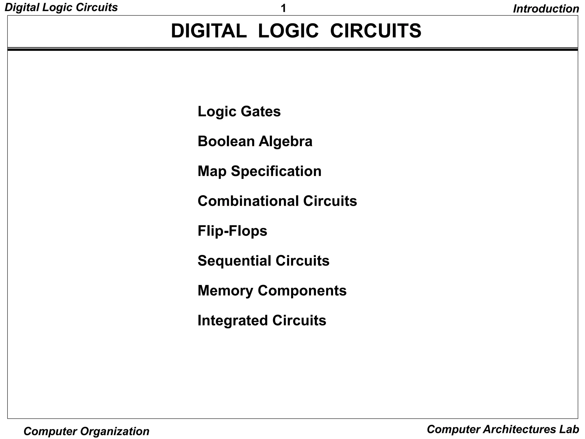
Digital Logic Circuits
Computer Organization Computer Architectures Lab
BASIC IDENTITIES OF BOOLEAN ALGEBRA
[1] x + 0 = x
[3] x + 1 = 1
[5] x + x = x
[7] x + x’ = 1
[9] x + y = y + x
[11] x + (y + z) = (x + y) + z
[13] x(y + z) = xy +xz
[15] (x + y)’ = x’y’
[17] (x’)’ = x
[2] x • 0 = 0
[4] x • 1 = x
[6] x • x = x
[8] x • X’ = 0
[10] xy = yx
[12] x(yz) = (xy)z
[14] x + yz = (x + y)(x + z)
[16] (xy)’ = x’ + y’
[15] and [16] : De Morgan’s Theorem
Usefulness of this Table
- Simplification of the Boolean function
- Derivation of equivalent Boolean functions
to obtain logic diagrams utilizing different logic gates
-- Ordinarily ANDs, ORs, and Inverters
-- But a certain different form of Boolean function may be convenient
to obtain circuits with NANDs or NORs
--> Applications of DeMorgans Theorem
x’y’ = (x + y)’ x’+ y’= (xy)’
I, AND --> NOR I, OR --> NAND
Boolean Algebra](https://image.slidesharecdn.com/computerarchitecture3rdeditionbymorismanoch01-ch02-231002085717-eb88c468/75/Computer-Architecture-3rd-Edition-by-Moris-Mano-CH-01-CH-02-ppt-7-2048.jpg)
![1
Digital Logic Circuits
Computer Organization Computer Architectures Lab
EQUIVALENT CIRCUITS
F = ABC + ABC’ + A’C .......…… (1)
= AB(C + C’) + A’C [13] ..…. (2)
= AB • 1 + A’C [7]
= AB + A’C [4] ...…. (3)
(1)
(2)
(3)
Many different logic diagrams are possible for a given Function
Boolean Algebra
A
B
C
F
A
B
C F
F
A
B
C](https://image.slidesharecdn.com/computerarchitecture3rdeditionbymorismanoch01-ch02-231002085717-eb88c468/75/Computer-Architecture-3rd-Edition-by-Moris-Mano-CH-01-CH-02-ppt-8-2048.jpg)


This document provides an overview of digital logic circuits. It begins with an introduction to logic gates and Boolean algebra. Common logic gates like AND, OR, NAND, NOR, XOR and XNOR are described along with their truth tables. Boolean algebra identities and theorems like De Morgan's theorem are discussed. Karnaugh maps are introduced as a method to simplify Boolean functions. The document describes how to implement logic functions from a Karnaugh map using sum-of-products form with AND and OR gates. Combinational and sequential circuits are also briefly mentioned.
This slide introduces digital logic circuits with topics like logic gates, Boolean algebra, and combinational/sequential circuits.
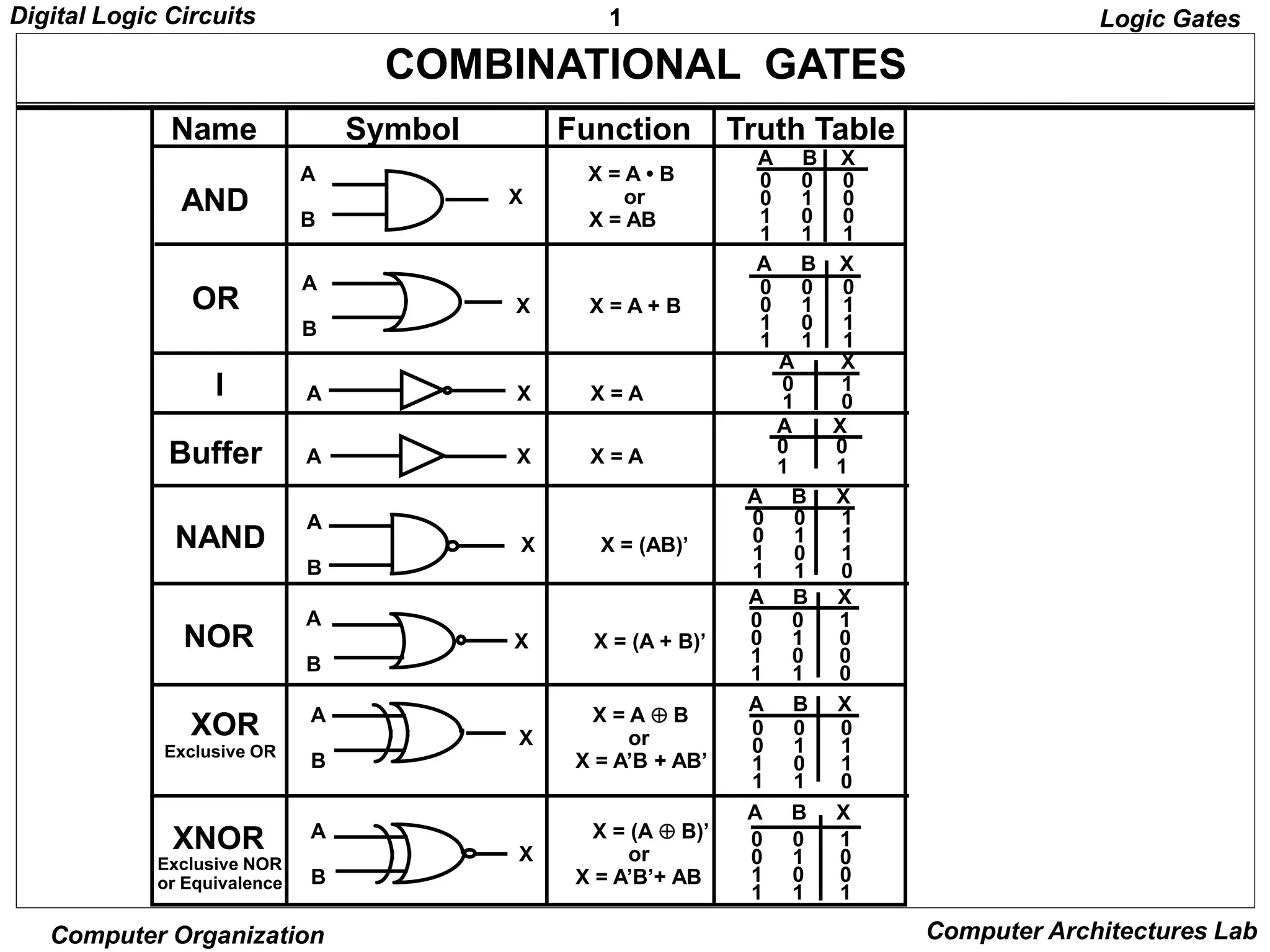
These slides explain digital logic's reliance on binary systems, basic types of logic gates including AND, OR, NOT, NAND, NOR, XOR, and XNOR.
The slides cover Boolean algebra principles, truth tables, and the process of deriving Boolean functions, including complements and simplifications.
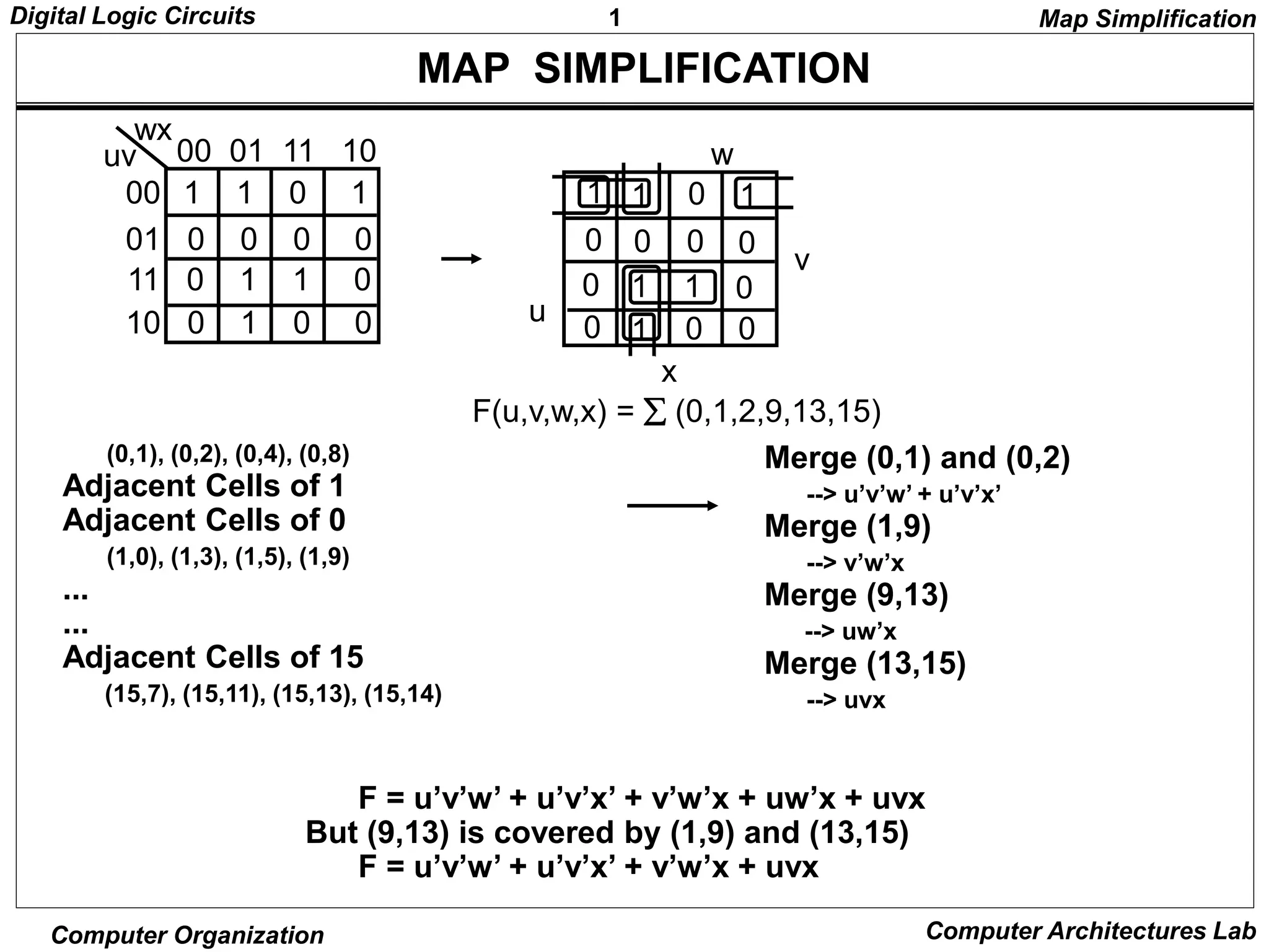
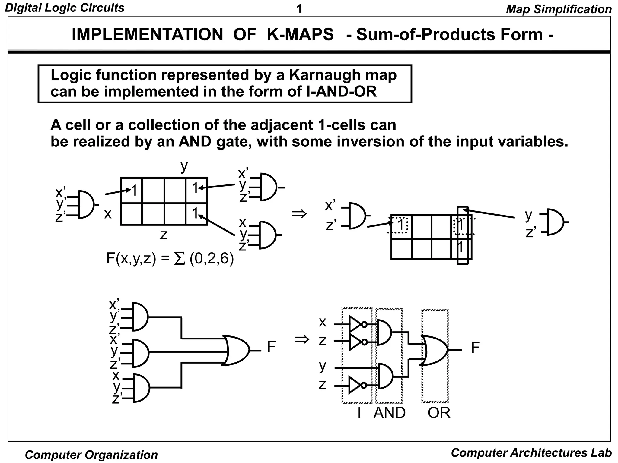
They detail the design process using truth tables and Karnaugh maps for simplifying Boolean expressions and deriving equivalent circuits.
These slides elaborate on using Karnaugh maps for simplification and implementation of logic functions including don't-care conditions.
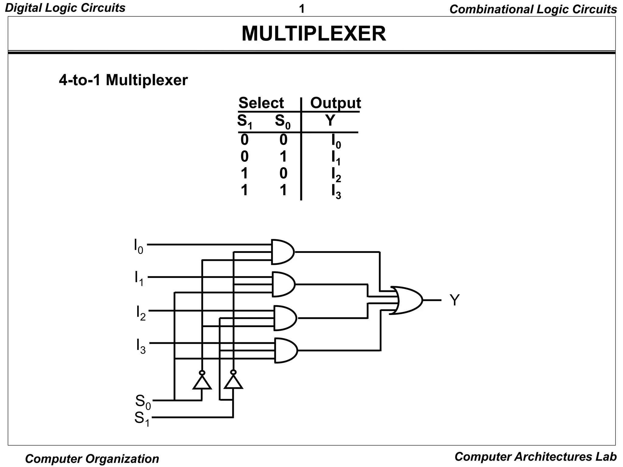
This section outlines combinational circuits, including adders (half and full), multiplexers, encoders, and decoders.
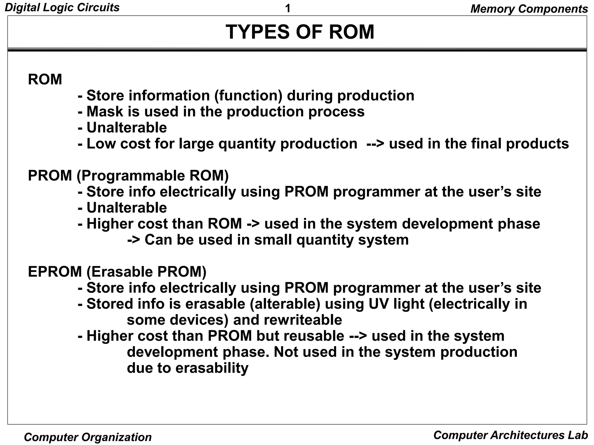
The final section discusses sequential circuits (like registers), various types of memory components including RAM and ROM, their characteristics and classifications.