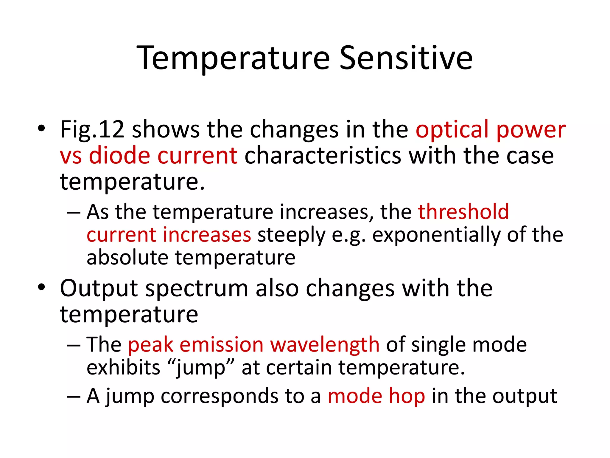
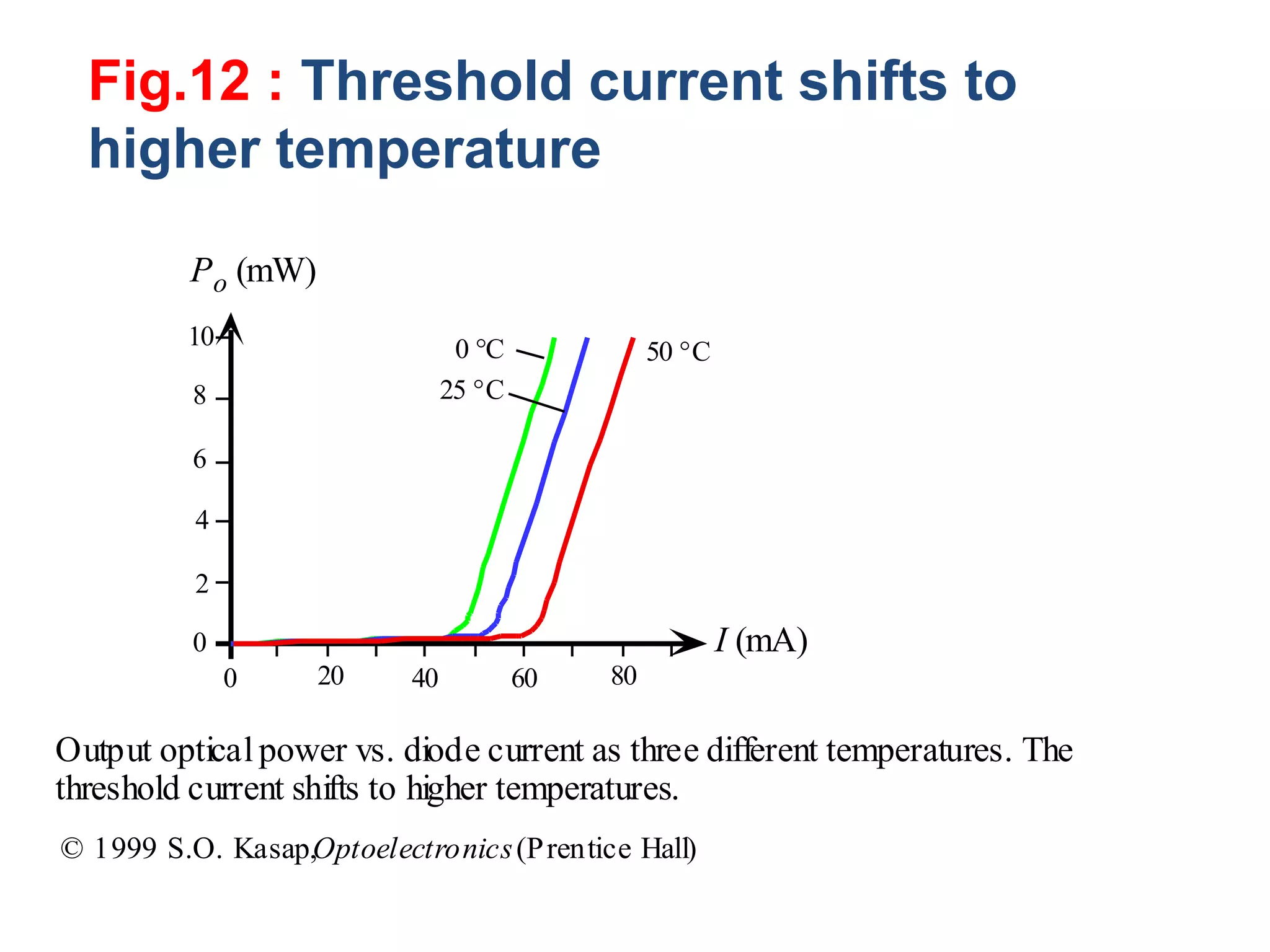
Downloaded 183 times
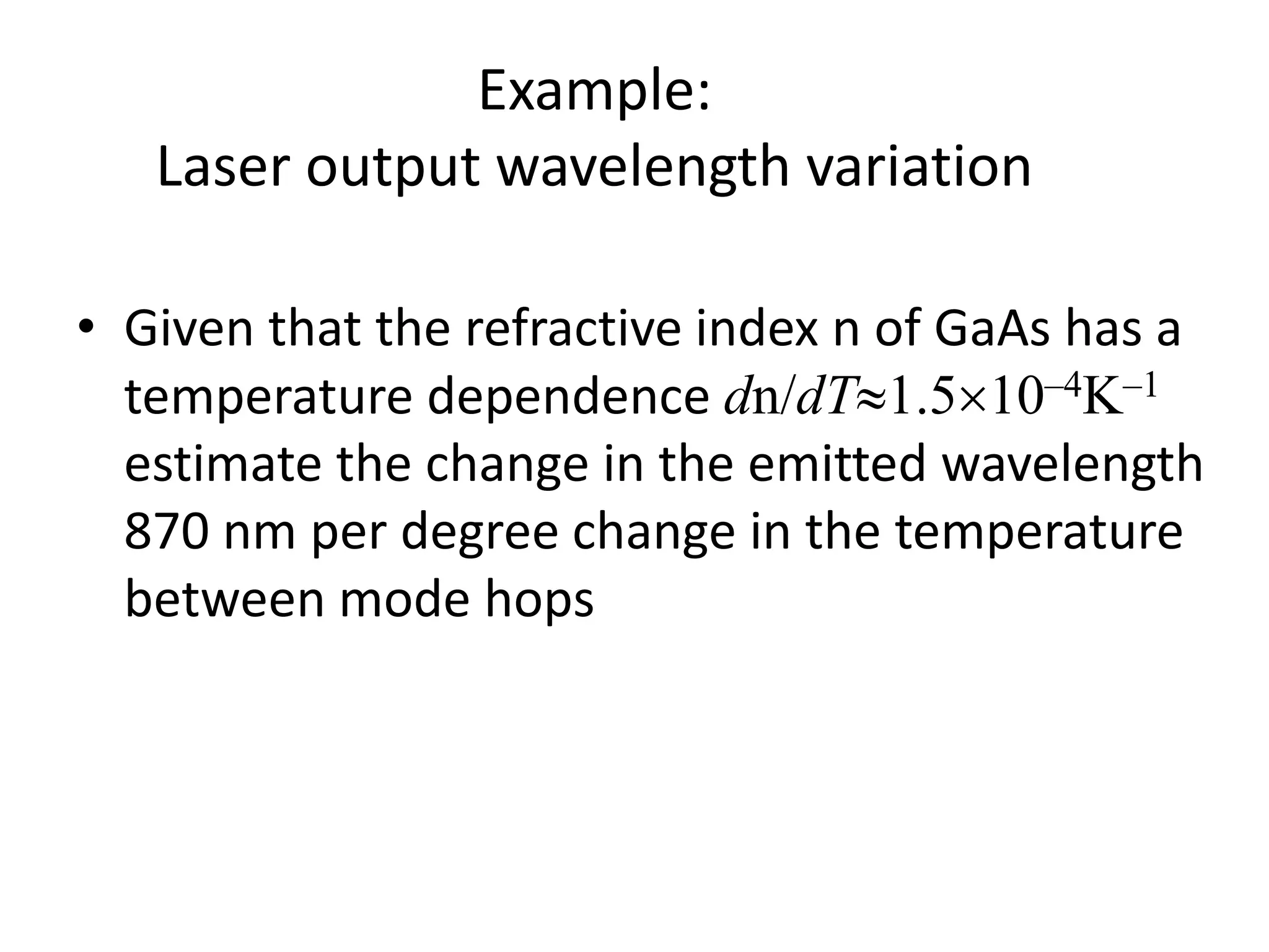
![Solution
• Consider a particular given mode with wavelength lm,
m (lm/2n) = L
dlm/dT = d/dT [2nL/m] 2 L/m (dn/dT)
Substituting for L/m in terms of lm,
dlm/dT lm/n (dn/dT)
=1.510–4K–1870nm/(3.7) =0.035nmK–1
Note that we used n for a passive cavity whereas n above should be
the effective refractive index of the active cavity which will also
depend on the optical gain of the medium, and hence its
temperature dependence is likely to be somewhat higher than the
dn/dt value we used](https://image.slidesharecdn.com/chapter5b-140705120950-phpapp02/75/Chapter-5b-31-2048.jpg)

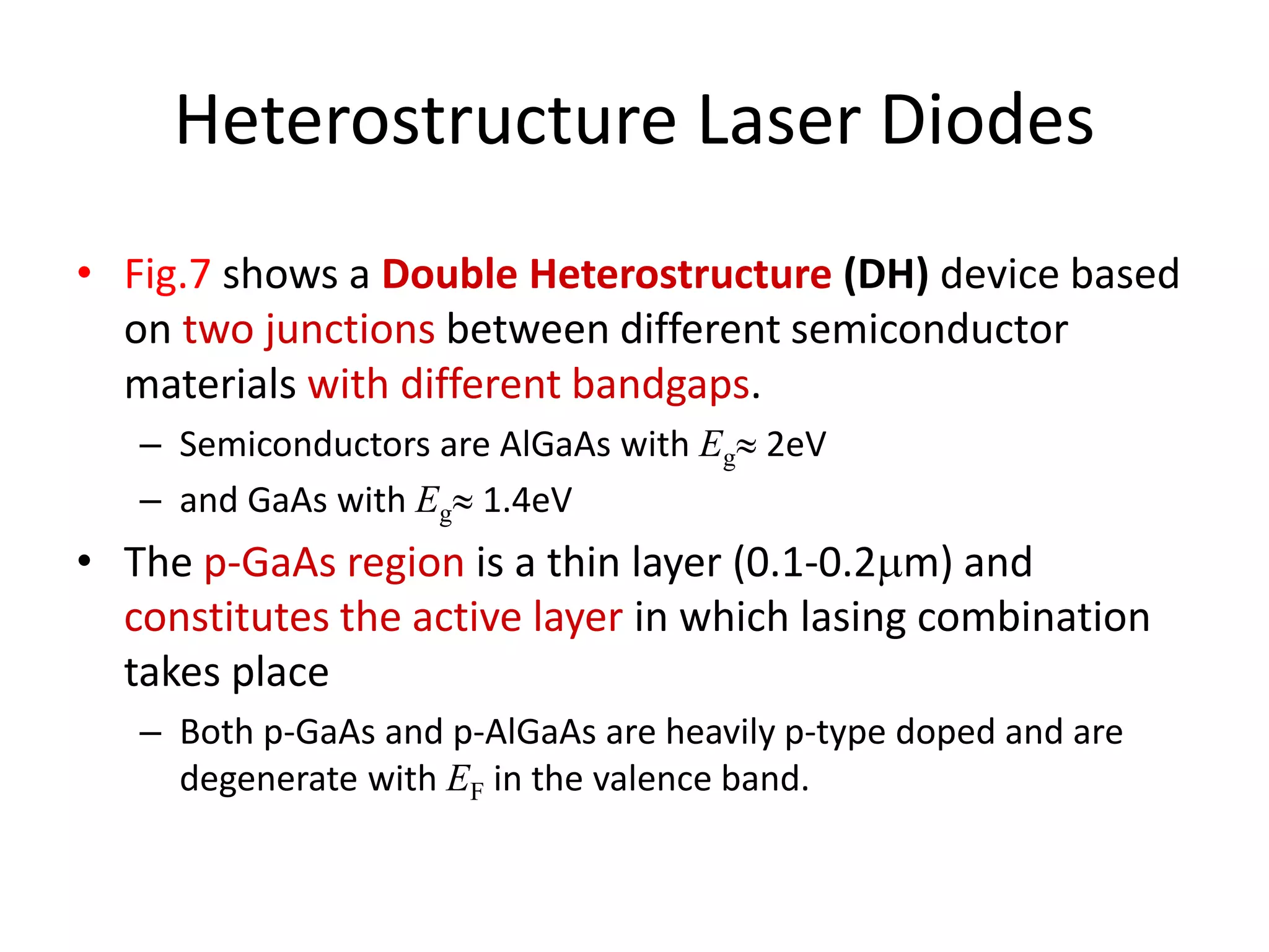
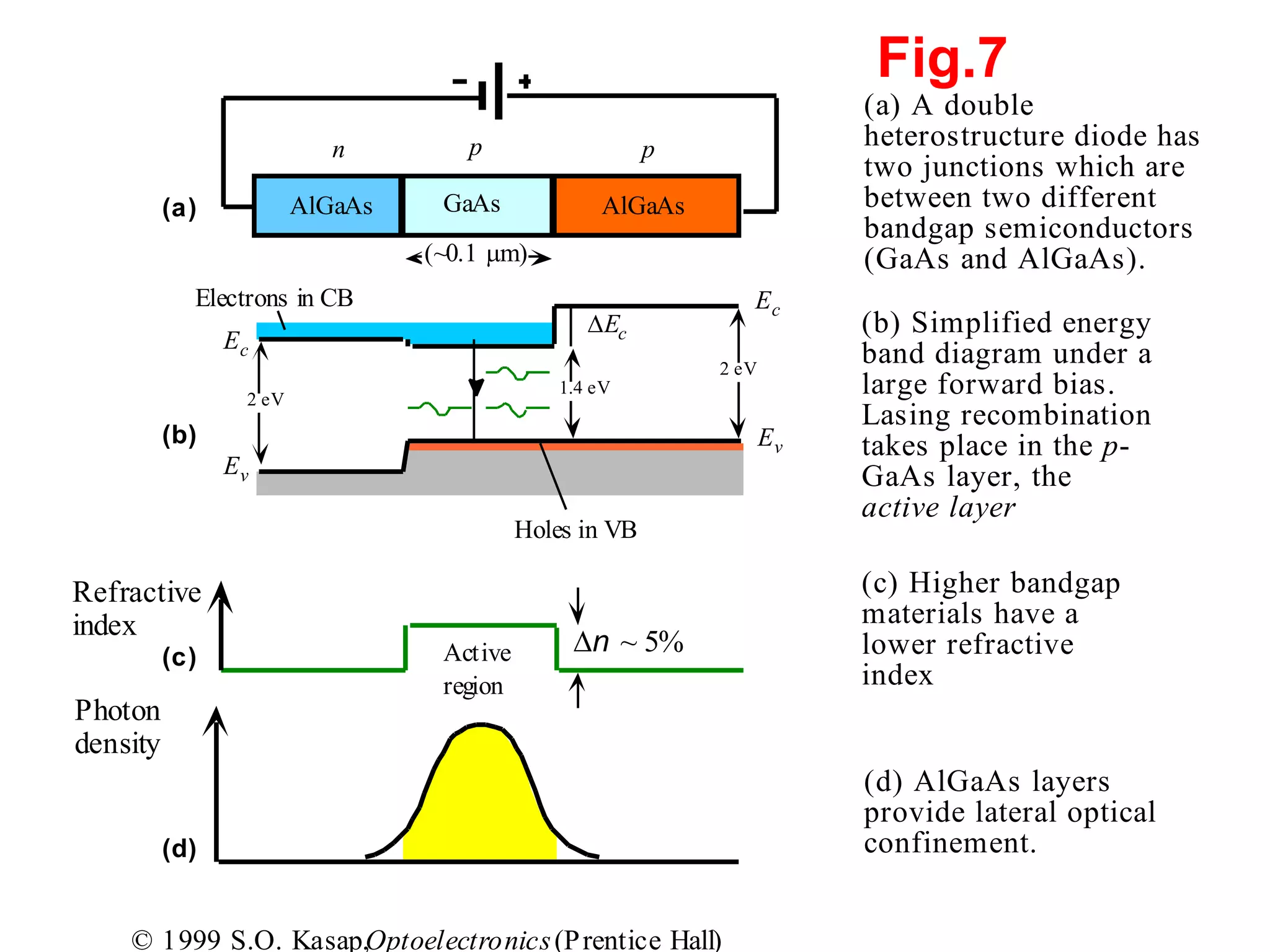
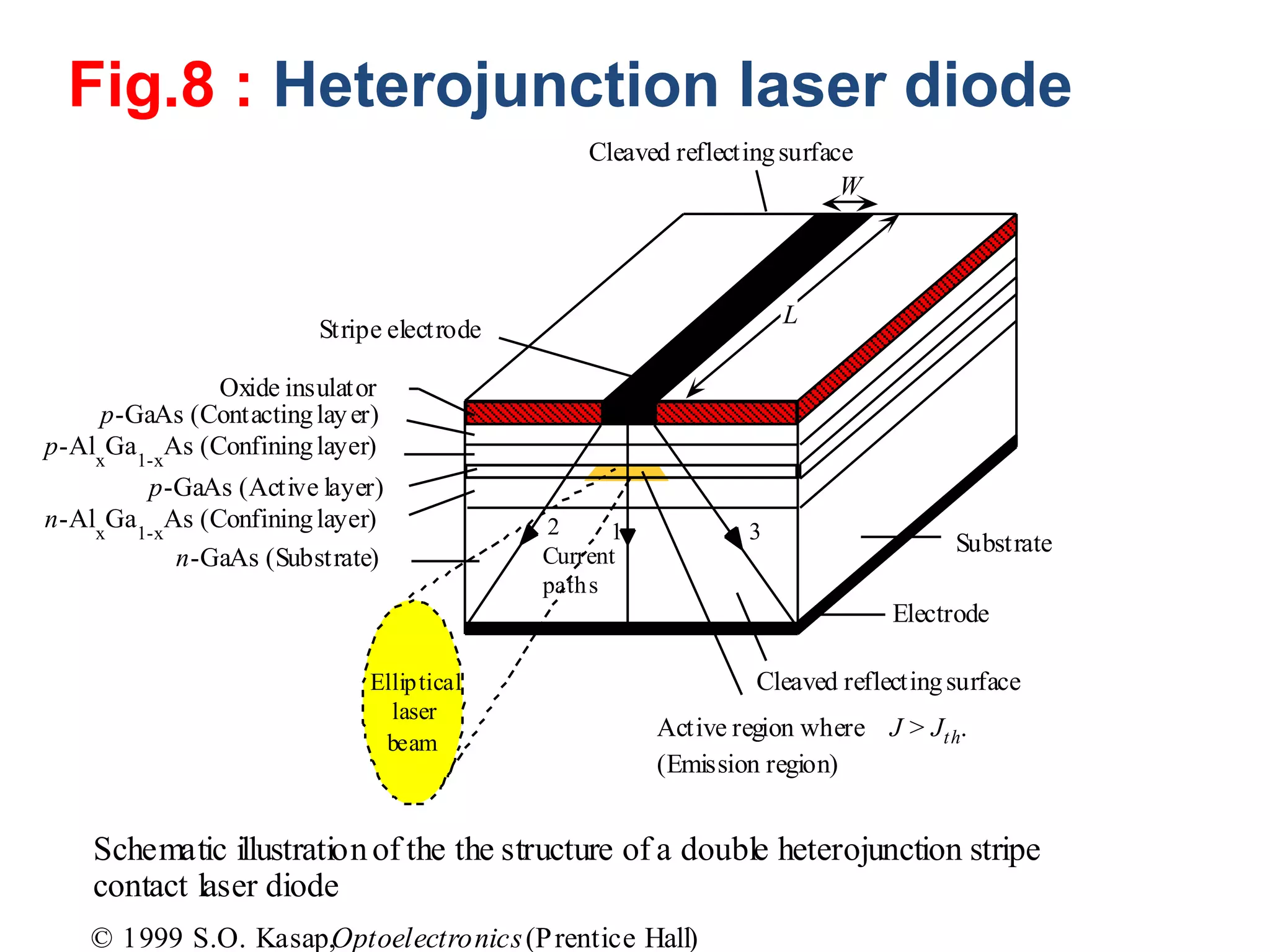
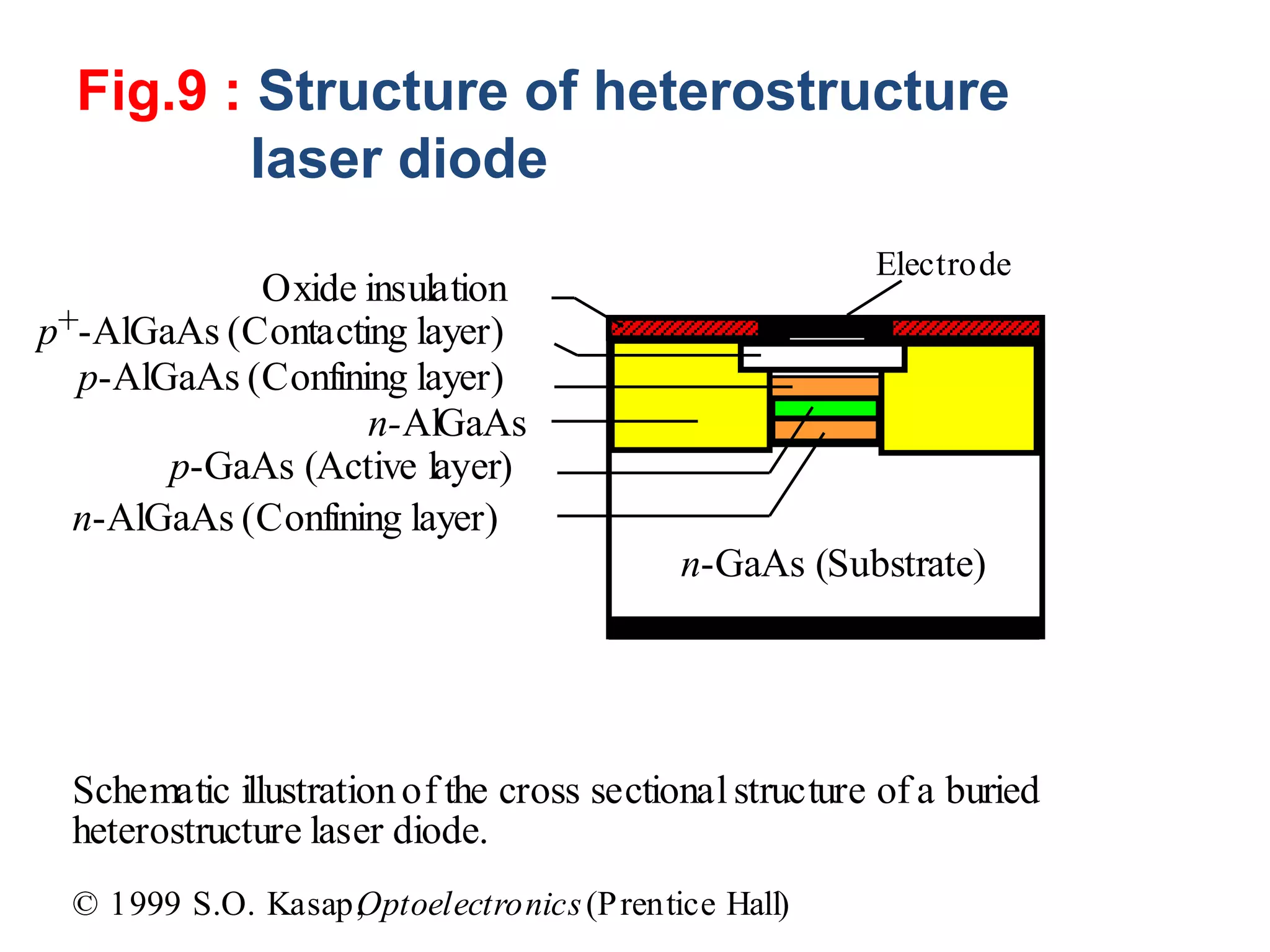
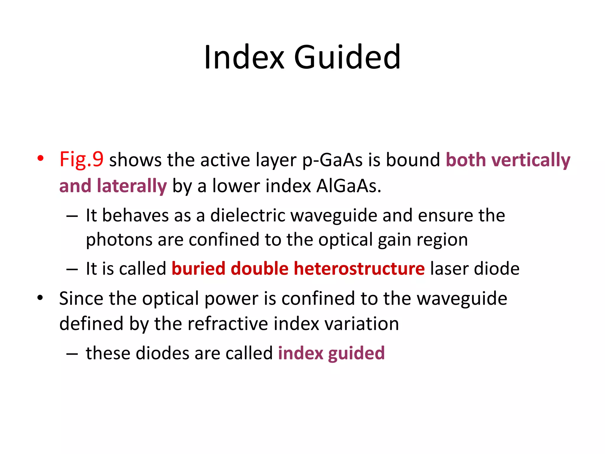
A double heterostructure laser diode consists of (1) a thin active GaAs layer sandwiched between (2) two AlGaAs confinement layers with a higher bandgap. Carriers and photons are confined to the active layer, reducing the threshold current density for lasing. The active layer provides optical gain while the confinement layers laterally guide photons via their lower refractive index. A stripe contact geometry further reduces threshold current and couples laser emission into optical fibers. Temperature increases the threshold current exponentially and can cause the emission wavelength to hop between longitudinal modes.