This document discusses AC-AC controllers that convert AC voltage from one form to another by varying amplitude, frequency, or phase. It describes:
- Single-phase and three-phase AC-AC controllers that control output waveform through switching electronic power devices.
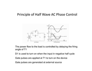
- Half-wave and full-wave phase control principles where the firing angle of thyristors controls power flow to the load.
- Equations to calculate output voltage, current, power factor for half-wave and full-wave controllers with resistive loads.
- Waveforms and operating principles of full-wave controllers, including discontinuous output and zero-average current when thyristors conduct equal times.
So in summary, it


![2
/
1
2
/
1
2
2
/
1
2
2
2
2
sin
1
2
)
(
)
2
cos
1
(
4
2
[
]
)
(
sin
2
2
1
[
)
(
+
−
=
−
=
=
∫
∫
α
α
π
π
ω
ω
π
ω
ω
π
π
α
π
α
s
s
s
Rms
V
t
d
t
V
t
td
V
sw
V
(5.4)
The average thyristor voltage:
The rms thyristor voltage:
( ) [ ] ( )
α
π
ω
π
ω
ω
π
π
α
π
α
cos
1
2
cos
2
sin
2
1
)
( +
=
−
=
= ∫ m
m
m
dc
V
t
V
t
td
V
sw
V
The average thyristor voltage:
(5.5)
R
sw
V
sw
I dc
dc
)
(
)
( =
R
sw
V
sw
I rms
rms
)
(
)
( =](https://image.slidesharecdn.com/chapter6-230622144207-62485464/85/Chapter-6-AC-AC-Converters-pdf-14-320.jpg)

![c) The average thyristor current
The PF is
(lagging)
707
.
0
2
.
1018
95
.
719
2
1
=
=
=
=
=
=
s
o
o
V
V
VA
P
PF
R
V
t
td
V
R
I
s
s
A
)
1
(cos
2
2
)
(
sin
2
2
1
+
+
+
+
=
=
=
=
=
=
=
= ∫
∫
∫
∫
α
α
α
α
π
π
π
π
ω
ω
ω
ω
ω
ω
ω
ω
π
π
π
π
π
π
π
π
α
α
α
α
d) The rms value of the thyristor current
A
R
7
.
2
10
2
120
2
2
=
=
=
=
=
=
=
=
π
π
π
π
π
π
π
π
A
x
R
V
t
d
t
R
V
t
td
V
R
I
s
s
s
R
6
10
2
120
2
2
sin
1
2
)
(
)
2
cos
1
(
4
2
[
]
)
(
sin
2
2
1
[
2
/
1
2
/
1
2
2
2
/
1
2
2
2
=
=
=
=
=
=
=
=
+
+
+
+
−
−
−
−
=
=
=
=
−
−
−
−
=
=
=
=
=
=
=
=
∫
∫
∫
∫
∫
∫
∫
∫
α
α
α
α
α
α
α
α
π
π
π
π
π
π
π
π
ω
ω
ω
ω
ω
ω
ω
ω
π
π
π
π
ω
ω
ω
ω
ω
ω
ω
ω
π
π
π
π
π
π
π
π
α
α
α
α
π
π
π
π
α
α
α
α](https://image.slidesharecdn.com/chapter6-230622144207-62485464/85/Chapter-6-AC-AC-Converters-pdf-16-320.jpg)


![Solution
the current is expressed from the parameters
A
m
V
rad
R
L
rad
R
L
L
R
Z
18
.
6
2
120
943
.
0
20
05
.
0
)
377
(
756
.
0
20
)
05
.
0
)(
377
(
1
tan
1
tan
5
.
27
2
)]
05
.
0
)(
377
[(
2
)
20
(
2
)
(
2
=
=
=
=
=
=
=
=
=
=
=
=
=
=
=
=
=
=
=
=
=
=
=
=
−
−
−
−
=
=
=
=
−
−
−
−
=
=
=
=
=
=
=
=
+
+
+
+
=
=
=
=
+
+
+
+
=
=
=
=
ω
ω
ω
ω
ωτ
ωτ
ωτ
ωτ
ω
ω
ω
ω
θ
θ
θ
θ
ω
ω
ω
ω
The current is then expressed as
The extinction angle β is determined from the numerical solution of i(β) = 0 in
the preceding equation
The conduction angle γ = β – α = 2.26 rad = 1300, which is less the the limit of
1800
A
e
Z
m
V
rad
A
Z
m
V
8
.
23
/
)
sin(
57
.
1
0
90
18
.
6
5
.
27
2
120
=
=
=
=
−
−
−
−
=
=
=
=
=
=
=
=
=
=
=
=
=
=
=
=
ωτ
ωτ
ωτ
ωτ
α
α
α
α
θ
θ
θ
θ
α
α
α
α
α
α
α
α
β
β
β
β
ω
ω
ω
ω
α
α
α
α
ωτ
ωτ
ωτ
ωτ
ω
ω
ω
ω
ω
ω
ω
ω ≤
≤
≤
≤
≤
≤
≤
≤
−
−
−
−
−
−
−
−
−
−
−
−
=
=
=
= t
for
943
.
0
/
8
.
23
)
756
.
0
sin(
18
.
6
)
(
0 A
e
t
t
i
0
220
83
.
3 =
=
=
=
=
=
=
= rad
β
β
β
β](https://image.slidesharecdn.com/chapter6-230622144207-62485464/85/Chapter-6-AC-AC-Converters-pdf-23-320.jpg)
![the rms load current is determined by
The rms current in each SCR is determine
[[[[ ]]]]
A
t
d
t
e
t
rms
I
71
.
2
83
.
3
57
.
1
)
(
2
943
.
0
/
8
.
23
)
756
.
0
sin(
18
.
6
1
,
0
=
=
=
=
∫
∫
∫
∫
−
−
−
−
−
−
−
−
−
−
−
−
=
=
=
= ω
ω
ω
ω
ω
ω
ω
ω
ω
ω
ω
ω
π
π
π
π
A
rms
o
I
rms
SCR
I 92
.
1
2
71
.
2
2
,
, =
=
=
=
=
=
=
=
=
=
=
=
the average SCR current is obtained
Power absorbed by the load
Power factor is determined from P/S
A
rms
SCR
I 92
.
1
2
2
, =
=
=
=
=
=
=
=
=
=
=
=
[[[[ ]]]]
A
t
d
t
e
t
avg
SCR
I
04
.
1
)
(
83
.
3
57
.
1
943
.
0
/
8
.
23
)
756
.
0
sin(
18
.
6
2
1
,
=
=
=
=
∫
∫
∫
∫
−
−
−
−
−
−
−
−
−
−
−
−
=
=
=
= ω
ω
ω
ω
ω
ω
ω
ω
ω
ω
ω
ω
π
π
π
π
W
R
rms
o
I
P 147
)
20
(
2
)
71
.
2
(
,
2 =
=
=
=
=
=
=
=
=
=
=
=
45
.
0
)
71
.
2
)(
120
(
147
,
,
=
=
=
=
=
=
=
=
=
=
=
=
=
=
=
=
rms
s
I
rms
s
V
P
s
P
pf](https://image.slidesharecdn.com/chapter6-230622144207-62485464/85/Chapter-6-AC-AC-Converters-pdf-24-320.jpg)