Download to read offline
![P. Anudeep et al Int. Journal of Engineering Research and Application
ISSN : 2248-9622, Vol. 3, Issue 6, Nov-Dec 2013, pp.382-385
RESEARCH ARTICLE
www.ijera.com
OPEN ACCESS
Design and Implementation of 2mbps Data and Voice Frame
Structure
P. Anudeep1, N. Vasudeva Reddy2
1, 2
M.Tech, Mlrit
Abstract
Most digital data are not stored in the most compact form. Rather, they are stored in whatever way makes them
easiest to use, such as: ASCII text from word processors, binary code that can be executed on a computer,
individual samples from a data acquisition system. The soft core allows the manipulation of E1(2Mbps)
2048KHz 32-channel carrier information. It inserts/removes data into/from E1 frame and multiframe structures.
The main use of the developed soft core in the implementation of data communication equipment is to allow
multiple users to share a common 2Mbps carrier with a flexible scheme for bandwidth allocation. The hardware
module that increases performance of the data communications.
KEYWORDS –2Mbps carrier frame, Drop_insert
I.
INTRODUCTION
Data compression is the general term for the
various algorithms and programs developed to
address this problem. A compression program is used
to convert data from an easy-to-use format to one
optimized
for
compactness.
Likewise,
an
uncompression program returns the information to its
original form.
A series of digital multiplexes graded
according to capability so that multiplexing at one
level combines a defined number of digital signals,
each having the digit rate prescribed for the next
lower order, into a digital signal having a prescribed
digit rate which is then available for further
combination with other digital signals of the same
rate in a digital multiplex of the next higher order.
The design implements the 2Mbps carrier
frame for adding and dropping for the scope of
individual enterprise users research & development.
The IP core is a complex, pre-designed and preverified hardware module that can be used in the
composition of large circuits, typically custom VLSI
integrated circuits or large programmable devices,
such as multimillion-gate FPGAs. The developed
software code in the form of hardware description
language file will support some applications & may
not support some functions due to synchronization at
the final implementation.
The developed design used for a telecom
applications in the form of E1 carrier transmission
www.ijera.com
protocol. The design operates dropping and adding
information from/to an E1 carrier frame, or simply
E1 frame. This hardware design respects the ITU-T
Standards G.703.
G.704 AND G.706 [1][2][3].The developed
module posed challenges in the synchronization of
data and control information. A dedicated IC to
mount an E1 frame and perform multiframe
alignment detection, Cyclic Redundancy Check
(CRC) computation and time slot detection. To
execute the add-drop function the usual solution is to
add a micro-controller. The hardware module used to
cascade several add-drop modules in a single
equipment. The next section describes the 2Mbps
frame structure . section 3 gives the hardware
implementation of the design for 2Mbps frame
structure. Section 4 gives the output waveforms of
each module. Section 5 presents a set of conclusions.
II.
Design and implementation of E1
Carrier Frame Structure
2.1 E1 multi Frame Structure
E1 is the lowest level of the Plesiochronous
Digital Hierarchy (PDH). It is among the most
common ways of transmitting voice and data over
telephone and data networks. The signal transported
in an E1 carrier allows the transmission of up to 31
voice or data channels plus 1channel dedicated to
carry low level control information
382 | P a g e](https://image.slidesharecdn.com/bm36382385-131122002341-phpapp02/85/Bm36382385-1-320.jpg)

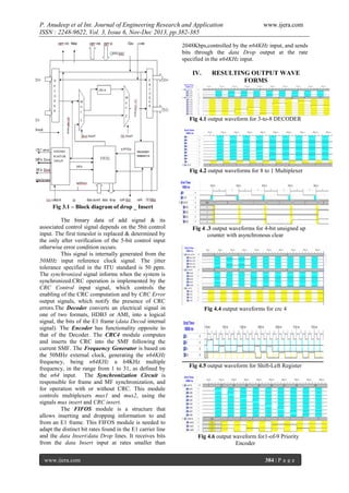
![P. Anudeep et al Int. Journal of Engineering Research and Application
ISSN : 2248-9622, Vol. 3, Issue 6, Nov-Dec 2013, pp.382-385
www.ijera.com
Fig 4.7 output waveform for Synchronization
circuit
V.
CONCLUSION
The hardware module designed for the adddrop functions of 2Mbps carriers. For better solution
than in the current availability in the VLSI design.
The timing constraints in the implementation were
not critical in the design. The only timing restriction
that posed some problem to be fulfilled was the n64
frequencies generation with the jitter tolerance
specified in the ITU standard, namely 50 ppm.
REFERENCES
[1]
[2]
[3]
[4]
[5]
[6]
[7]
[8]
BERGAMASCHI, R. A.; LEE, W. R.
Designing systerns-on--chip using cores.
37th Design
Automation
Conference, 2000, pp. 420-425
SEMICONDUCTOR
INDUSTRY
ASSOCIATION – SIA: 'International
Technology Roadmap for Semiconductors
2002
Update'.
http://public.itrs.net/Files/2002Update/Home
.pdf
XILINX, INC: ‘Investor Factsheet - Third
Quarter
Fiscal
Year
2003’.
http://www.xilinx.com
VAHID, F.; GIVARGIS, T.: 'Platform
tuning for embedded systems design'. IEEE
Computer, 2001, 34 (3) pp. 112-114
ITU-T: 'Physical/electrical characteristics of
hierarchical
digital
interfaces'.
Recommendation G.703, 1998
ITU-T: 'Synchronous frame structures used
at 1544, 6312, 2048, 8448 and 44736 kbit/s
hierarchical
levels'.
Recommendation
G.704, 1998
ITU-T: 'Frame alignment and cyclic
redundancy check (CRC) procedures
relating to basic frame structures defined in
Recommendation G.704'. Recommendation
G.706, 1991
DALLAS SEMICONDUCTOR. 'DS21354
and DS21554 E1 Single Chip Transceivers'.
Data Sheet. 2003. http://www.dalsemi.com
www.ijera.com
385 | P a g e](https://image.slidesharecdn.com/bm36382385-131122002341-phpapp02/85/Bm36382385-4-320.jpg)

The document presents the design and implementation of a 2Mbps data and voice frame structure aimed at optimizing data storage and facilitating bandwidth allocation in communication systems. It discusses a soft core for manipulating E1 frame structures, detailing the challenges of synchronization and CRC computation within the data transmission process. The hardware design conforms to ITU-T standards and incorporates a drop-insert function that dynamically modifies E1 frames for real-time data communication.