Download to read offline


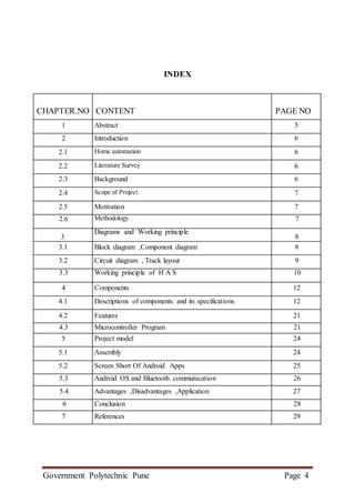
![Government Polytechnic Pune Page 5
1. ABSTRACT
Technology is a never ending process. To be able to design a product using the current
technology that will be beneficial to the lives of others is a huge contribution to the community. This
paper presents the design and implementation of a low cost but yet flexible and secure cell phone
based home automation system. The design is based on a stand alone BT board and the home
appliances are connected to the input/ output ports of this board via relays. The communication
between the cell phone and the BT board is wireless. This system is designed to be low cost and
scalable allowing variety of devices to be controlled with minimum changes to its core. Password
protection is being used to only allow authorised users from accessing the appliances at home.
The project is designed to operate electrical loads using relays interfaced to a microcontroller
through remotely operated commands to it by touch screen based user friendly GUI on any smart
phone with Android applications. 8 Channel Android Bluetooth Projects is great for controlling your
devices over Bluetooth link without any RF design knowledge. This module is designed to plug in to
your design seamlessly. Individual relay can be controlled by simple commands. [9]
The project is designed to operate relay/electrical loads using an Android application device. The
system operates electrical loads depending on the data transmitted from the Android application
device. Operating conventional wall switches is difficult for elderly or physically handicapped people.
This proposed system solves the problem by integrating house hold appliances to a control unit that
can be operated by an Android smart-phone/Tablet etc.
Remote operation is achieved by any smart-phone/Tablet etc., with Android OS, upon a GUI
(Graphical User Interface) based touch screen operation, interfaced to the microcontroller of 8051
family. The program on the microcontroller serially communicates with Bluetooth device to generate
respective output based on the input data (sent from Android application device) to operate a set of
relays through a relay driver IC. The loads are interfaced to the control unit through the relays. The
system can be used in existing domestic area for either operating the loads through conventional
switches.[10]](https://image.slidesharecdn.com/finalsaif-converted-200705172313/85/BLUETOOTH-BASED-HOME-AUTOMATION-SYSTEM-5-320.jpg)
![Government Polytechnic Pune Page 6
2.INTRODUCTION
Wireless technologies are becoming more popular around the world and the consumers appreciate
this wireless lifestyle which gives them relive of the well known “cable chaos” that tends to grow
under their desk. Now with the embedded Bluetooth technology, digital devices form a network in
which the appliances and devices can communicate with each other. Today, home automation is one of
the major applications of Bluetooth technology. Operating over unlicensed, globally available
frequency of 2.4GHz, it can link digital devices within a range of 10m to 100m at the speed of up to
3Mbps depending on the Bluetooth device class. With this capability of Bluetooth; we propose a
home automation system based on Bluetooth technology
There are few issues involved when designing a home automation system. The system should be
scalable so that new devices can easily be integrated into it. It should provide a user- friendly interface
on the host side, so that the devices can be easily setup, monitored and controlled. This interface
should also provide some diagnostic services so that if there is any problem with the system, it can be
tracked down. Moreover the overall system should be fast enough to realize the true power of wireless
technology. Finally the system should be cost effective in order to justify its application in home
automation. This method provides facility to the computer user to control the home appliances without
walk to the switches on the wall. Third control method is done by Android GUI installed in Smart
Phone. The user can easily touch on the screen of the phone to control the home appliances. This
portable method is able to assist the disabled people who have problem with locomotion difficulty[7]
2.1. Home automation -
Home automation may designate an emerging practice of increased automation of household
appliances and features in residential dwellings, particularly through electronic means that allow for
things impracticable, overly expensive or simply not possible in recent decades. Home automation
includes all that a building automation provides like climate controls, door and window controls, and
in addition control of multimedia home theatres, pet feeding, plant watering and so on. But there
exists a difference in that home automation emphasizes more on comforts through ergonomics and
ease of operation [2]
2.2. Literature Survey-
Bluetooth based home automation system using cell phones: In Bluetooth based home automation
system the home appliances are connected to the BT board at input output ports using relay. The
program of BT board is based on high level interactive C language of microcontrollers; the connection
is made via Bluetooth. The password protection is provided so only authorized user is allowed to
access the appliances. The Bluetooth connection is established between BT board and phone for
wireless communication. In this system the python script is used and it can install on any of the
Symbian OS environment, it is portable. One circuit is designed and implemented for receiving the
feedback from the phone, which indicate the status of the device.[3]
2.3. Background –
The “Home Automation” concept has existed for many years. The terms “Smart Home”,
“Intelligent Home” followed and has been used to introduce the concept of networking appliances and
devices in the house. Home automation Systems (HASs) represents a great research opportunity in
creating new fields in engineering, and Computing. HASs includes centralized control of lighting,
appliances, security locks of gates and doors and other systems, to provide improved comfort, energy
efficiency and security system. HASs becoming popular nowadays and enter quickly in this emerging
market. However, end users, especially the disabled and elderly due to their complexity and cost, do
not always accept these systems. Due to the advancement of wireless technology, there are several
different of connections are introduced such as GSM, WIFI, and Bluetooth. Each of the connection has](https://image.slidesharecdn.com/finalsaif-converted-200705172313/85/BLUETOOTH-BASED-HOME-AUTOMATION-SYSTEM-6-320.jpg)
![Government Polytechnic Pune Page 7
their own unique specifications and applications. Among the four popular wireless connections that
often implemented in HAS project, WIFI is being chosen with its suitable capability. The capabilities
of WIFI are more than enough to be implemented in the design. Also, most of the current
laptop/notebook or Smartphone come with built-in WIFI adapter. It will indirectly reduce the cost of
this system. This project forwards the design of home automation and security system using Raspberry
pi, a credit sized computer. Raspberry pi provides the features of a mini computer, additional with its
GPIO pins where other components and devices can be connected. GPIO registers of raspberry pi are
used for the output purposes. We have design a power strip that can be easily connected to GPIO Pins
of the Raspberry pi. The home appliances are connected to the input/output ports of Raspberry pi
along with the power strip and their status is passed to the raspberry pi. The android running OS in any
phone connected to a network can access the status of the home appliances via an application. It
presents the design and implementation of automation system that can monitor and control home
appliances via android phone or tablet.[7]
2.4. Scope of Project –
The project aims at designing a prototype for controlling the home appliances that can be controlled
wirelessly via an application that provides the features of speech recognition, video streaming, and
switch mode. An application is run on android device. The system can be used in wide range of areas.
The system integrated with different features can be applied in the following fields
. • The system can be used in home, small offices to the big malls The system can be used from home
to offices to control the electrical appliances.
• For remote access of appliances in internet or intranet. The home/office appliances can be controlled
in intra-network or can be accessed via internet.
• For the development of technology friendly environment The system incorporates the use of
technology and making smart home automation. By the use of day to day gadgets we can utilize them
for different prospective.[5]
2.5. Motivation -
This project work is complete on its own in remotely and automatically switching on and off of any
electrical appliance not limited to household appliances, and sends a feedback message indicating the
new present state of the appliance. It does not implement control of multiple appliances or automatic
detection of faults in the controlled appliance[5]
1. Home Automation is a growing trend
2. Make common home appliances and media accessible to disabled
3. Safer home
4. Always had an interest in home automation
5. A simple way to manage multiple end points by the average user using a smartphone
2.6. Methodology – (Assembly)
Use the component overlay on the PCB to place the components starting with the lowest height
components first. Make sure that the diode, LED and electrolytic capacitors are inserted the right way
around.
First check the components in the Kit against the Component listing. Identify all the components. It is
generally best to solder the lowest height components first: the IC SOCKETS, resistors, & diodes. The
IC socket should be installed first. Begin solders the pin of the socket. The entire resistor should be
installed next. In order to find their values you have to check the color code. All the diode should be
installed next. Make sure to get the diodes the correct way around. Match up the bar on the diodes with
the bar on the overlay. Afterwards solder the capacitors, transistors, & other remaining components.
Especially care should be taken in order to find the polarity of the electrolytic capacitors.[10]](https://image.slidesharecdn.com/finalsaif-converted-200705172313/85/BLUETOOTH-BASED-HOME-AUTOMATION-SYSTEM-7-320.jpg)
![Government Polytechnic Pune Page 8
3. Block diagram and Working principle
Figure3.1.1 Block diagram for Home Automation system.[8]
Figure 3.1.2 PCB Layout for home automation system[8]](https://image.slidesharecdn.com/finalsaif-converted-200705172313/85/BLUETOOTH-BASED-HOME-AUTOMATION-SYSTEM-8-320.jpg)
![Government Polytechnic Pune Page 9
Figure 3.2.1 Circuit Diagram for Home Automation System [9]
Figure 3.2.1 PCB Track Layout For Home Automation System [5]](https://image.slidesharecdn.com/finalsaif-converted-200705172313/85/BLUETOOTH-BASED-HOME-AUTOMATION-SYSTEM-9-320.jpg)
![Government Polytechnic Pune Page 10
3.3 Working Principle of Home Automation System
Remote operation is achieved by any smart-phone/Tablet etc., with Android OS, upon a GUI
(Graphical User Interface) based touch screen operation, interfaced to the microcontroller of 8051
family. The program on the microcontroller serially communicates with Bluetooth device to generate
respective output based on the input data (sent from Android application device) to operate a set of
relays through a relay driver IC. The loads are interfaced to the control unit through the relays. The
system can be used in existing domestic area for either operating the loads through conventional
switches. See the block diagram of unite. Is based on AT89C2051 (20 Pin) Micro controller. The
complete [8]
projects divided in different interfacing part
1. Main micro controller unite, use as CPU
2. Bluetooth Module Interfacing
3. Relay driver & Relay Section
4. Regulated power supply
3.3.1 MICRO CONTROLLER INTERFACE
The full circuit of the Android Remote controlled switch is shown in circuit diagramed. The brain
of the switcher is the Atmel AT89C2051 micro controller (U1). This project is mainly based on mobile
phone communication with the Microcontroller through Bluetooth. Connect the Bluetooth module
with microcontroller using the serial port communication. This board has eight on board 12V DC
relays that can switch up to 5A load. The relays are controlled by a MCU over Bluetooth link. [6]
3.3.1.1 MCU Cock
Clock signal for the micro controller provided by crystal X1 (11.0592 MHZ) and two 33PF (C4, C5)
capacitors hanging off it ensure correct loading for the crystal, so that it starts reliably. The frequency
of the oscillator is internally divided and to get the operating frequency. This high frequency clock
source is used to control the sequencing of CPU instruction.
3.3.1.2 MCU Reset
Power on reset is provided by R13 and C1. The 89C2051 micro controller has an active high reset
signal
3.3.2 BLUETOOTH INTERFACE
To connect the Bluetooth device, will required UART / Serial Connection, MCU AT89C2051 Have
the Rx and TX pins on Port pin P3.0 (RXD) and P3.1 (TXD). Rx pin from Bluetooth device to the TX
pin on the microcontroller, and the TX pin from Bluetooth device to the Rx pin on the microcontroller
. [7]
3.3.3 Relay Driver
The micro controller controls the outputs over port P1. The relay requires 12 volts at a current of
around 100 ma, which cannot provided by the micro controller. So the driver IC is added. The most
commonly available driver chip which ULN2803, we are used. A single pole dabble throw (SPDT)
relay is connected to port P1.0 to P1.7 of the micro controller through a Relay driver IC (ULN2803 –
U3). The relay is used to operate the external high Voltage Load or appliance or any other electrical
device. Normally the relay remains off. As soon as pin of the micro controller goes high, the relay
operates. LED L1 to L8 indicates relay status . LED has a current limiting resistor in series. The LED /
resistor combination is simply in parallel with the relay The relay contacts are rated at 10 amps.
However the PCB tracks can only take around 5 amps. You may need to add wire links on the bottom
of the PCB to increase the current carrying capacity if you want to draw over 5A. The relay outputs are
rated to switch up to 240VAC mains voltages. [5]](https://image.slidesharecdn.com/finalsaif-converted-200705172313/85/BLUETOOTH-BASED-HOME-AUTOMATION-SYSTEM-10-320.jpg)
![Government Polytechnic Pune Page 11
3.3.3.1Relay Connection
Figure 3.1 Output Relay Connection
The output of the projects is controlled by a relay, allowing any load until 230V AC / 3 Amp. As
maximum consumption. The relay has 3 output terminals the normally open at quiescent (NO), the
normally closed at quiescent (NC) and the common. The operating of this mechanism is the same as a
switch with two (2) terminals NO and common, if you wish that the output will be activated during the
timer, or between the NC and the common to obtain the reverse operating. In the drawing, you could
appreciate the typical connection for a devices operating at 12 VDC and to operate at 230 VAC.
When the project is working and according to its load, it could happen an incorrect operating of the
output. If it is the case, you have to install a circuit between 2 relay's contacts used for the connection.
See the drawing map.
Figure 3.2 Output Relay connection
3.3.3.2 External Outputs
Output (CN1 to CN4), Its controlled by a 12V SPDT relay and can switch up to 230V AC/DC This is
more than enough for all common signal sources such as Electronic lock, door strike, motor light or
any other appliances.
3.3.4 POWER SUPPLY
The power supply circuit. It’s based on 3 terminal voltage regulators, which provide the required
regulated +5V and unregulated +12V. Power is deliver initially from standard 12V AC/DC adapter or
12V_800ma Transformer. This is fed to bridge rectifier (Diode D1 ~ 4) the output of which is then
filtered using 1000uf electrolytic capacitor and fed to U4 (voltage regulator). U4 +5V output powers
the micro controller and other logic circuitry. LED L9 and its associate 1K (R9) current limiting
resistors provide power indication. The unregulated voltage of approximately 12V is required for
relay, and Relay Driver IC. [5]](https://image.slidesharecdn.com/finalsaif-converted-200705172313/85/BLUETOOTH-BASED-HOME-AUTOMATION-SYSTEM-11-320.jpg)
![Government Polytechnic Pune Page 12
4 COMPONENTS
Descriptions of Components and its Specifications and Features (Hardware)-
List of main components used-[4]
R1 ~ 9 - 1K [BROWN, BLACK, RED] (9 NOS)
R13 - 10K [BROWN, BLACK, ORANGE]
RN1 - 10K – 9 Pin Resistor bank (R-Pack)
C1 - 10UF / 16V Electrolytic
C4, 5 – 33PF Ceramic Disc (2 NOS)
C6 - 1000UF / 16V Electrolytic
C8, 9 - 100KPF DISC (0.1UF / 104) (2 NOS)
X1 - 11.0592 MHZ Crystal
D1 ~ 4 - 1N4007 Diode (4 NOS)
L1 ~ 8 - 3 mm OR 5 mm RED LED (8 NOS)
L9 - 3 mm OR 5 mm GREEN LED
U1 - AT89C2051 - MICROCONTROLLER (Pre Programmed MCU)
U2 - HK4U Serial Blue tooth Module
U3 - ULN2803 Relay Driver IC
U4 - LM7805 - +5V Voltage Regulator
1 nos - 20 PIN IC SOCKET FOR U1
1 nos - 18 PIN IC SOCKET FOR U3
RL1 ~ 8 - 12V PCB MOUNT SPDT RELAY [8 nos]
CN1 ~ 8 - 3 PIN SCREW TERMINALS BLOCK (8 NOS) not
CN9 - 2 PIN SCREW TERMINALS BLOCK
Software
_ Any Android phone
_ Android app (BT voice Control for Android for voice commands )
Main Components Specifications and Features
4.1.1 MICRO CONTROLLER AT89C2051
The AT89C2051 is a low-voltage, high-performance CMOS 8-bit microcomputer with 2K bytes of
Flash programmable and erasable read-only memory (PEROM). The device is manufactured using
Atmel’s high-density nonvolatile memory technology and is compatible with the industry-standard
MCS-51 instruction set. By combining a versatile 8-bit CPU with Flash on a monolithic chip, the
Atmel AT89C2051 is a powerful microcomputer which provides a highly-flexible and cost-effective
solution to many embedded control applications.[1]
Fig.4.1 MICRO CONTROLLER AT89C2051](https://image.slidesharecdn.com/finalsaif-converted-200705172313/85/BLUETOOTH-BASED-HOME-AUTOMATION-SYSTEM-12-320.jpg)
![Government Polytechnic Pune Page 13
FEATURES
• Compatible with MCS®-51Products
• 2K Bytes of Reprogrammable Flash Memory
• 2.7V to 6V Operating Range
• Two-level Program Memory Lock
• 128 x 8-bit Internal RAM
• 15 Programmable I/O Lines
• Two 16-bit Timer/Counters
• Six Interrupt Sources
• Programmable Serial UART Channel
• Direct LED Drive Outputs
• On-chip Analog Comparator
4.1.1.2Description
The AT89C2051 is a low-voltage, high-performance CMOS 8-bit microcomputer with 2K bytes of Flash
programmable and erasable read-only memory (PEROM). The device is manufactured using Atmel’s high-
density nonvolatile memory technology and is compatible with the industry-standard MCS-51 instruction set.
By combining a versatile 8-bit CPU with Flash on a monolithic chip, the Atmel AT89C2051 is a power-full
microcomputer which provides a highly-flexible and cost-effective solution to many embedded control
applications. The AT89C2051 provides the following standard features: 2K bytes of Flash, 128 bytes of RAM,
15 I/O lines, two 16-bit timer/counters, a five vector two-level interrupt architecture, a full duplex serial port, a
precision analog comparator, on-chip oscillator and clock circuitry. In addition, the AT89C2051 is designed
with static logic for opera-tion down to zero frequency and supports two software selectable power saving
modes. The Idle Mode stops the CPU while allowing the RAM, timer/counters, serial port and interrupt system
to continue functioning. The power-down mode saves the RAM contents but freezes the oscillator disabling all
other chip functions until the next hardware reset. [1]
4.1.1.3Pin Configuration
Fig. 4.2 Pin Configuration
4.1.1.4 Pin Description
VCC Supply voltage.
GND Ground.
Port 1 The Port 1 is an 8-bit bi-directional I/O port. Port pins P1.2 to P1.7 provide internal pull-ups.
P1.0 and P1.1 require external pull-ups. P1.0 and P1.1 also serve as the positive input (AIN0) and the
negative input (AIN1), respectively, of the on-chip precision analog comparator. The Port 1 out-put
buffers can sink 20 mA and can drive LED displays directly. When 1s are written to Port 1 pins, they
can be used as inputs. When pins P1.2 to P1.7 are used as inputs and are externally pulled low, they
will source current (IIL) because of the internal pull-ups. Port 1 also receives code data during Flash](https://image.slidesharecdn.com/finalsaif-converted-200705172313/85/BLUETOOTH-BASED-HOME-AUTOMATION-SYSTEM-13-320.jpg)
![Government Polytechnic Pune Page 14
programming and verification. [1]
Port 3 Port 3 pins P3.0 to P3.5, P3.7 are seven bi-directional I/O pins with internal pull-ups. P3.6 is
hard-wired as an input to the output of the on-chip comparator and is not accessible as a gen-eral-
purpose I/O pin. The Port 3 output buffers can sink 20 mA. When 1s are written to Port 3 pins they are
pulled high by the internal pull-ups and can be used as inputs. As inputs, Port 3 pins that are externally
being pulled low will source current (IIL) because of the pull-ups.
Port 3 also serves the functions of various special features of the AT89C2051 as listed below
Port Pin Alternate Functions
P3.0 RDX (serial input port)
P3.1 TXD (serial output port )
P3.2 INT0 (external interrupt 0 )
P3.3 INT1 (external interrupt 1)
P3.4 T0 (timer 0 external input)
P3.5 T1 (timer 1 external input)
Port 3 also receives some control signals for Flash programming and verification.
RST Reset input. All I/O pins are reset to 1s as soon as RST goes high. Holding the RST pin high for
two machine cycles while the oscillator is running resets the device. Each machine cycle takes 12
oscillator or clock cycles.
XTAL1 Input to the inverting oscillator amplifier and input to the internal clock operating circuit.
XTAL2 Output from the inverting oscillator amplifier.
Crystal oscillator
A crystal oscillator is an electronic circuit that uses the mechanical resonance of a vibrating crystal of
Piezoelectric material to create an electrical signal with a very precise frequency. This frequency is
commonly used to keep track of time (as in quartz wristwatches), to provide a stable clock signal for
digital integrated circuits, and to stabilize frequencies for radio transmitters/receivers. [3]
Fig 4.3 Crystal Oscillator
Oscillator Characteristics The XTAL1 and XTAL2 are the input and output, respectively, of an
inverting amplifier which can be configured for use as an on-chip oscillator, as shown in Figure 5-1.
Either a quartz crystal or ceramic resonator may be used. To drive the device from an external clock
source, XTAL2 should be left unconnected while XTAL1 is driven as shown in Figure 5-2. There are
no require-ments on the duty cycle of the external clock signal, since the input to the internal clocking](https://image.slidesharecdn.com/finalsaif-converted-200705172313/85/BLUETOOTH-BASED-HOME-AUTOMATION-SYSTEM-14-320.jpg)
![Government Polytechnic Pune Page 15
circuitry is through a divide-by-two flip-flop, but minimum and maximum voltage high and low time
specifications must be observed.[4]
Figure 4.4 Crystal Oscillator Connection [4]
Figure 4.5 External Clock Drive configuration
Figure 4.6 Programming the Flash Memory [4]](https://image.slidesharecdn.com/finalsaif-converted-200705172313/85/BLUETOOTH-BASED-HOME-AUTOMATION-SYSTEM-15-320.jpg)
![Government Polytechnic Pune Page 16
Figure 4.7 Verifying the flash Memory [4]
Figure 4.8 Dimension of Pin [4]
4.1.2 ULN2803A (Relay driver IC) (HIGH-VOLTAGE, HIGH-CURRENT DARLINGTON
ARRAYS)
The ULN2803 is high voltage, high current Darlington arrays each containing eight open collector
Darlington pairs with common emitters . Each channel rated at 500 mA and can withstand peak
currents of 600 mA. Suppression diodes are included for inductive load driving and the inputs are
pinned opposite the outputs to simplify board layout. These versatile devices are useful for driving a
wide range of loads including solenoids, relays DC motors; LED displays filament lamps, thermal
printer heads and high power buffers.](https://image.slidesharecdn.com/finalsaif-converted-200705172313/85/BLUETOOTH-BASED-HOME-AUTOMATION-SYSTEM-16-320.jpg)
![Government Polytechnic Pune Page 17
Fig. 4.9 ULN2803A (Relay driver IC)
Featuring continuous load current ratings to 500 mA for each of the drivers, the Series
ULN28xxA/LW and ULQ28xxA/LW highvoltage, high-current Darlington arrays are ideally suited
for interfacing between low-level logic circuitry and multiple peripheral power loads. Typical power
loads totaling over 260 W (350 mA x 8, 95 V) can be controlled at an appropriate duty cycle
depending on ambient temperature and number of drivers turned ON simultaneously. Typical
loads include relays, solenoids, stepping motors, magnetic print hammers, multiplexed LED and
incandescent displays, and heaters. All devices feature open-collector outputs with integral clamp
diodes. [4]
The ULx2803A, ULx2803LW, ULx2823A, and ULN2823LW have series input resistors selected for
operation directly with 5 V TTL or CMOS. These devices will handle numerous interface needs
particularly those beyond the capabilities of standard logic buffers. The ULx2804A, ULx2804LW,
ULx2824A, and ULN2824LW have series input resistors for operation directly from 6 V to 15 V
CMOS or PMOS logic outputs
The ULx2803A/LW and ULx2804A/LW are the standard Darlington arrays. The outputs are capable
of sinking 500 mA and will withstand at least 50 V in the OFF state. Outputs may be paralleled for
higher load current capability.
The ULx2823A/LW and ULx2824A/ LW will withstand 95 V in the OFF state. These Darlington
arrays are furnished in 18-pin dual in-line plastic packages (suffix ‘A’) or 18-lead small-outline plastic
packages (suffix ‘LW’). All devices are pinned with outputs opposite inputs to facilitate ease of circuit
board layout. Prefix ‘ULN’ devices are rated for operation over the temperature range of -20°C to
+85°C; prefix ‘ULQ’ devices are rated for operation to -40°C.
Figure 4.10 Dimension of ULN2803A (Relay driver IC) in Inches](https://image.slidesharecdn.com/finalsaif-converted-200705172313/85/BLUETOOTH-BASED-HOME-AUTOMATION-SYSTEM-17-320.jpg)
![Government Polytechnic Pune Page 18
FEATURES
n TTL, DTL, PMOS, or CMOS Compatible Inputs
n Output Current to 500 mA
n Output Voltage to 95 V
n Transient-Protected Outputs
n Dual In-Line Package or Wide-Body Small-Outline Package
4.1.3 LM7805 (3 TERMINAL VOLTAGE REGULATER)
This is used to make the stable voltage of +5V for circuits. The LM7805 is three terminal positive
regulators are available in the TO-220 - package and with several fixed output voltages, making them
useful in a wide range of applications. Each type employs internal current limiting, thermal shut down
and safe operating area protection, making it essentially indestructible. If adequate heat sinking is
provided, they can deliver over 1A output current. Although designed primarily as fixed voltage
regulators, [4]
Fig 4.11 LM7805 (3 TERMINAL VOLTAGE REGULATER)
4.1.4 Bluetooth Module
This module enables you to wireless transmit & receive serial data. It is a drop in replacement for
wired serial connections allowing transparent two way data communication. You can simply use it for
serial port replacement to establish connection between MCU or embedded project and PC for data
transfer .Main module operates on 3V only. This board operates on 5V and has LED indication and 3V
regulator onboard. [7]
Features
5V power operation
UART interface
10 meters range
Easy to use
Minimum External Components
Status LEDs
Fig 4.12 Bluetooth Module](https://image.slidesharecdn.com/finalsaif-converted-200705172313/85/BLUETOOTH-BASED-HOME-AUTOMATION-SYSTEM-18-320.jpg)
![Government Polytechnic Pune Page 19
Applications
Wireless Telemetry
Remote control & automation syste
Remote Data Logging
Robotics
Sensor Networks
Remote Programming
Specifications
Bluetooth protocol v2.0
Range 10 meters
Frequency: 2.4 Ghz ISM
Modulation: GFSK
Transmit power: 4dBm
Sensitivity: 84dBm
Rate: 2.1Mbps(Max) /160kbps(Async); 1Mbps(Sync)
Authentication & Encryption
Module only Power Supply: +3.3 VDC 50mA
Operating Temperate: -20C to +55 C
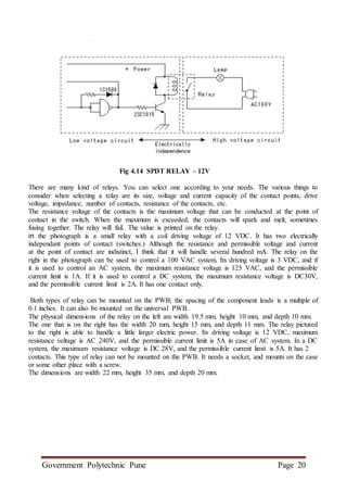
4.1.5 SPDT RELAY – 12V
It closes the voltage less point of contact while the remote control works to control the equipment
outside. The relay takes advantage of the fact that when electricity flows through a coil, it becomes an
electromagnet. The electromagnetic coil attracts a steel plate, which is attached to a switch. So the
switch's motion (ON and OFF) is controlled by the current flowing to the coil,or not, respectively. A
very useful feature of a relay is that it can be used to electrically isolate different parts of a circuit. It
will allow a low voltage circuit (e.g. 5VDC) to switch the power in a high voltage circuit (e.g. 230
VAC or more). The relay operates mechanically, so it cannot operate at high speed.
Figure 4.13 Relay
The relay takes advantage of the fact that when electricity flows through a coil, it becomes an
electromagnet. The electromagnetic coil attracts a steel plate, which is attached to a switch. So the
switch's motion (ON and OFF) is controled by the current flowing to the coil, or not, respectively. A
very useful feature of a relay is that it can be used to electrically isolate different parts of a circuit. It
will allow a low voltage circuit (e.g. 5VDC) to switch the power in a high voltage circuit (e.g. 100
VAC or more). The relay operates mechanically, so it can not operate at high speed. [4]](https://image.slidesharecdn.com/finalsaif-converted-200705172313/85/BLUETOOTH-BASED-HOME-AUTOMATION-SYSTEM-19-320.jpg)
![Government Polytechnic Pune Page 21
4.2 Features
4.2.1 Voice Command
The project will have an android application in the user's android device. This application is
designed to receive the voice commands from the user. The application will the automatically convert
the voice signals into digital data and send these signals to the microcontroller. [10]
4.2.2 Smart Speech Sense
The application will be coded as such to decode the meaning of any statement from the user. The user won't
be restricted to use of any particular command set. He would just have to state out his problem the application
will itself sense the meaning of the user's speech convert it into respective available command.[10]
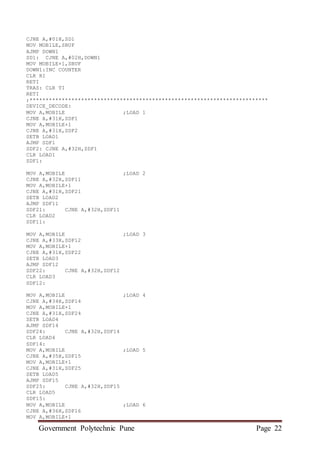
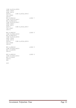
4.3 Microcontroller Program [6] [8]
LOAD1 EQU P1.0
LOAD2 EQU P1.1
LOAD3 EQU P1.2
LOAD4 EQU P1.3
LOAD5 EQU P1.4
LOAD6 EQU P1.5
LOAD7 EQU P1.6
LOAD8 EQU P1.7
DSEG ; This is internal data memory
ORG 20H ; Bit adressable memory
MOBILE: DS 3
COUNTER: DS 1
CSEG
ORG 00H ; Reset
AJMP MAIN
ORG 0023H
AJMP SERIAL
MAIN: MOV SP,#40H
MOV TMOD,#20H
MOV TH1,#0FDH
MOV SCON,#50H
MOV IE,#10010000B
SETB TR1
MOV COUNTER,#00H
MOV P1,#00H
AJMP $
;**************************************************************************
SERIAL:
JB TI,TRAS1
MOV A,SBUF
CJNE A,#'A',DOWNW
MOV COUNTER,#00H
AJMP DOWN1
TRAS1: AJMP TRAS
DOWNW:CJNE A,#0AH,DOWNW1
CALL DEVICE_DECODE
AJMP DOWN1
DOWNW1:MOV A,COUNTER](https://image.slidesharecdn.com/finalsaif-converted-200705172313/85/BLUETOOTH-BASED-HOME-AUTOMATION-SYSTEM-21-320.jpg)
![Government Polytechnic Pune Page 24
5 Project Modle
Fig 5 project model
5.1 Assembly
Use the component overlay on the PCB to place the components starting with the lowes height
components first. Make sure that the diode , LED and electrolytic capacitors are inserted the right
Way around.
First check the components in the Kit against the Component listing. Identify all the
components. It is generally best to solder the lowest height components first: the IC SOCKETS,
resistors, & diodes. The IC socket should be installed first. Begin solders the pin of the socket. The
entire resistor should be installed next. In order to find their values you have to check the color code.
All the diode should be installed next. Make sure to get the diodes the correct way around. Match up
the bar on the diodes with the bar on the overlay. Afterwards solder the capacitors, transistors, LED
display & other remaining components. Especially care should be taken in order to find the polarity of
the electrolytic capacitors. [6]
Use the component overlay on the PCB to place the components in the following order
Note: - Please before assemble the kit; please see the PCB Overlay / photograph / demonstration
video of assembled projects. (on google)
1. Resistors and diodes
2. IC sockets
3. Ceramic capacitors.
4. LM7805 regulators. Use needle nosed pliers to bend the leads of the regulator. It does not
require heat sink. Screw down onto to PCB.
5. Crystal, and LED’s
6. Electrolytic capacitors. Make sure you insert them the correct way around.
7. Screw Terminal blocks. Note the terminal blocks do NOT slide together. Also make sure the
wire entry side faces out from the PCB.
8. Bluetooth Module (Make sure you insert them the correct way around or check PCB overlay
9. Relay’s](https://image.slidesharecdn.com/finalsaif-converted-200705172313/85/BLUETOOTH-BASED-HOME-AUTOMATION-SYSTEM-24-320.jpg)
![Government Polytechnic Pune Page 26
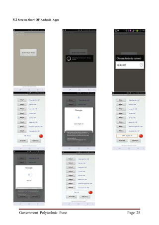
5.3 Android OS (operating systen) And Bluetooth communicatin
5.3.1 Android OS
Android is an operating system based on the Linux kernel , and designed primarily for touch screen
mobile devices such as smart phones and tablet computers. The user interface of Android is based off
direct manipulation, using touch inputs that loosely correspond to real-world actions , like swiping,
tapping, pinching and reverse pinching to manipulate on-screen objects. Internal hardware.
Android is the world's most widely used smart phone platform, overtaking Symbian in the fourth
quarter of 2010. Android is popular with technology companies who require a ready-made, low-cost,
customizable and lightweight operating system for high tech devices. Despite being primarily designed
for phones and tablets, it has been also used in televisions, games consoles, digital cameras and other
electronics. Android's open nature has encouraged a large community of developers and enthusiasts to
use the open-source code as a foundation for community-driven projects, which add new features for
advanced users or bring Android to devices which were officially, released running other operating
systems. [9]
5.3.2 Bluetooth communication
Bluetooth is a wireless technology standard for exchanging data over short distances (using short
wavelength radio transmissions in the ISM band from 2400–2480 MHz) from fixed and mobile
devices, creating personal area networks (PANs) with high levels of security. it was originally
conceived as a wireless alternative to RS-232 data cables. It can connect several devices, overcoming
problems of synchronization
Bluetooth technology is a short-range communications technology that is simple, secure, and
everywhere. You can find it in billions of devices ranging from mobile phones and computers to
medical devices and home entertainment products. It is intended to replace the cables connecting
devices, while maintaining high levels of security. The key features of Bluetooth technology are
robustness, low power, and low cost. The Bluetooth Specification defines a uniform structure for a
wide range of devices to connect and communicate with each other. When two Bluetooth enabled
devices connect to each other, this is called pairing. The structure and the global acceptance of
Bluetooth technology means any Bluetooth enabled device, almost everywhere in the world, can
connect to other Bluetooth enabled devices located in proximity to one another.
Connections between Bluetooth enabled electronic devices allow these devices to communicate
wirelessly through short-range, ad hoc networks known as piconets. Piconets are established
dynamically and automatically as Bluetooth enabled devices enter and leave radio proximity meaning
that you can easily connect whenever and wherever it's convenient for you. Each device in a piconet
can also simultaneously communicate with up to seven other devices within that single piconet and
each device can also belong to several piconets simultaneously. This means the ways in which you can
connect your Bluetooth devices is almost limitless. A fundamental strength of Bluetooth wireless
technology is the ability to simultaneously handle data and voice transmissions. which provides users
with a variety of innovative solutions such as hands-free headsets for voice calls, printing and fax
capabilities, and synchronization for PCs and mobile phones, just to name a few.The range of
Bluetooth technology is application specific. The Core Specification mandates a minimum range of 10
meters or 30 feet, but there is no set limit and manufacturers can tune their implementations to provide
the range needed to support the use cases for their solutions.[7]](https://image.slidesharecdn.com/finalsaif-converted-200705172313/85/BLUETOOTH-BASED-HOME-AUTOMATION-SYSTEM-26-320.jpg)
![Government Polytechnic Pune Page 27
5.4 Advantages / Disadvantages ,Application
5.4.1 Advantages
1. The in efficiency of operation of conventional wall switches can be overwhelmed using various
home automation systems.
2. The loss of power can be reduced and manpower required for home automation is very less
compared to
conventional methods.
3. The IR, RF, android application, Bluetooth, DTMF, etc., based home automation systems can
be more efficient, provides ease of operation.
4. Provides safety from electrical power short circuits while using conventional wall switches to
operate loads.
5. Home automation system with automated door locking and security cameras facilitates more
security.
6. save a lot of time to operate home appliances from anywhere [5]
5.4.2 Disadvantages
1. Slow
2. Limited communication possible
3. Not in the trend
4. Not robust at all
5. Bluetooth is used in this home automation system, which have a range of 10 to 20 meters so the
control cannot be achieved from outside this range.
6. Application is connected after disconnect of the Bluetooth.
7. When the new users want to connect, first download application software and then configuration
must be done. [5]
5.4.3 Applications
1. Industrial Automation System
2. Electricity GRID Control & Monitoring
3. Supervision and monitoring alarm systems;
4. Industrial or domestic power management
5. Street light management
6. Home automation
7. Load shedding
8. Pumping Stations, Tanks, Oil or Water levels;
9. Weather Stations;
10. River Monitoring and Flood Control
11. Valve controls;
12. Unmanned machine rooms;
13. Control room application; [9]](https://image.slidesharecdn.com/finalsaif-converted-200705172313/85/BLUETOOTH-BASED-HOME-AUTOMATION-SYSTEM-27-320.jpg)
![Government Polytechnic Pune Page 28
6 CONCLUSIONS
In this paper we have introduced design and implementation of a low cost, flexible and
wireless solution to the home automation. The system is secured for access from any user or
intruder. The users are expected to acquire pairing password for the BT and the cell phone to
access the home appliances. This adds a protection from unauthorized users. This system can be
used as a test bed for any appliances that requires on-off switching applications without any
internet connection.
The full functionality of the home automation system was tested and the wireless communication
between the cell phone and BT was found to be limited to <50m in a concreted building and
maximum of 100m range was reported to be applicable in an open range.
Right now the Symbian OS cell phones only support Python scripts. For future work it is
recommended to develop the application for the cell phone to be written in Java so that it can
be supported by most of the cell phones available nowadays. [9]
-](https://image.slidesharecdn.com/finalsaif-converted-200705172313/85/BLUETOOTH-BASED-HOME-AUTOMATION-SYSTEM-28-320.jpg)

The document presents a project report on a Bluetooth-based home automation system designed by Shaikh Saif Fayaj as part of his electrical engineering diploma at Government Polytechnic, Pune. It outlines the system's architecture, functionality, components, and methodology, emphasizing scalability, user-friendliness, and accessibility for individuals with mobility challenges. The project utilizes a microcontroller for relay control, enabling remote operation of household appliances via an Android application, enhancing convenience and safety in home automation.