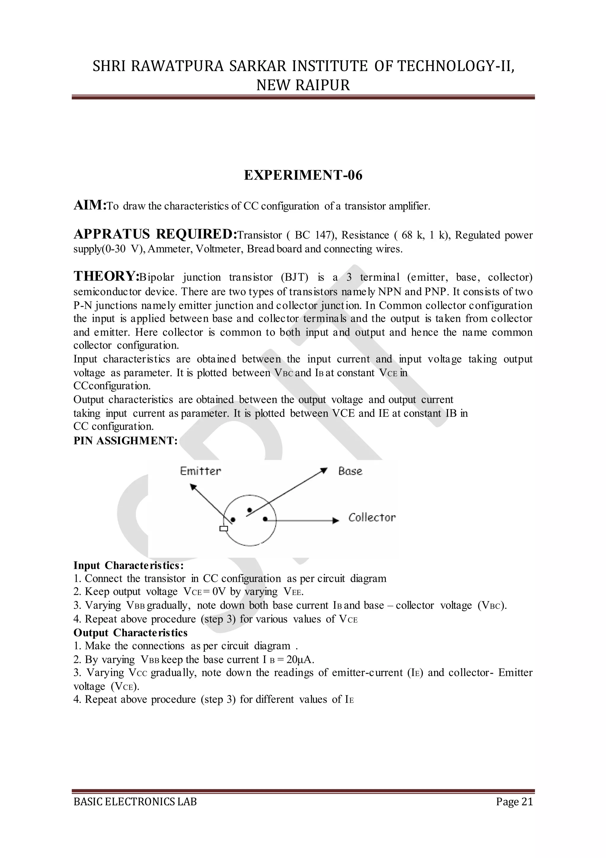
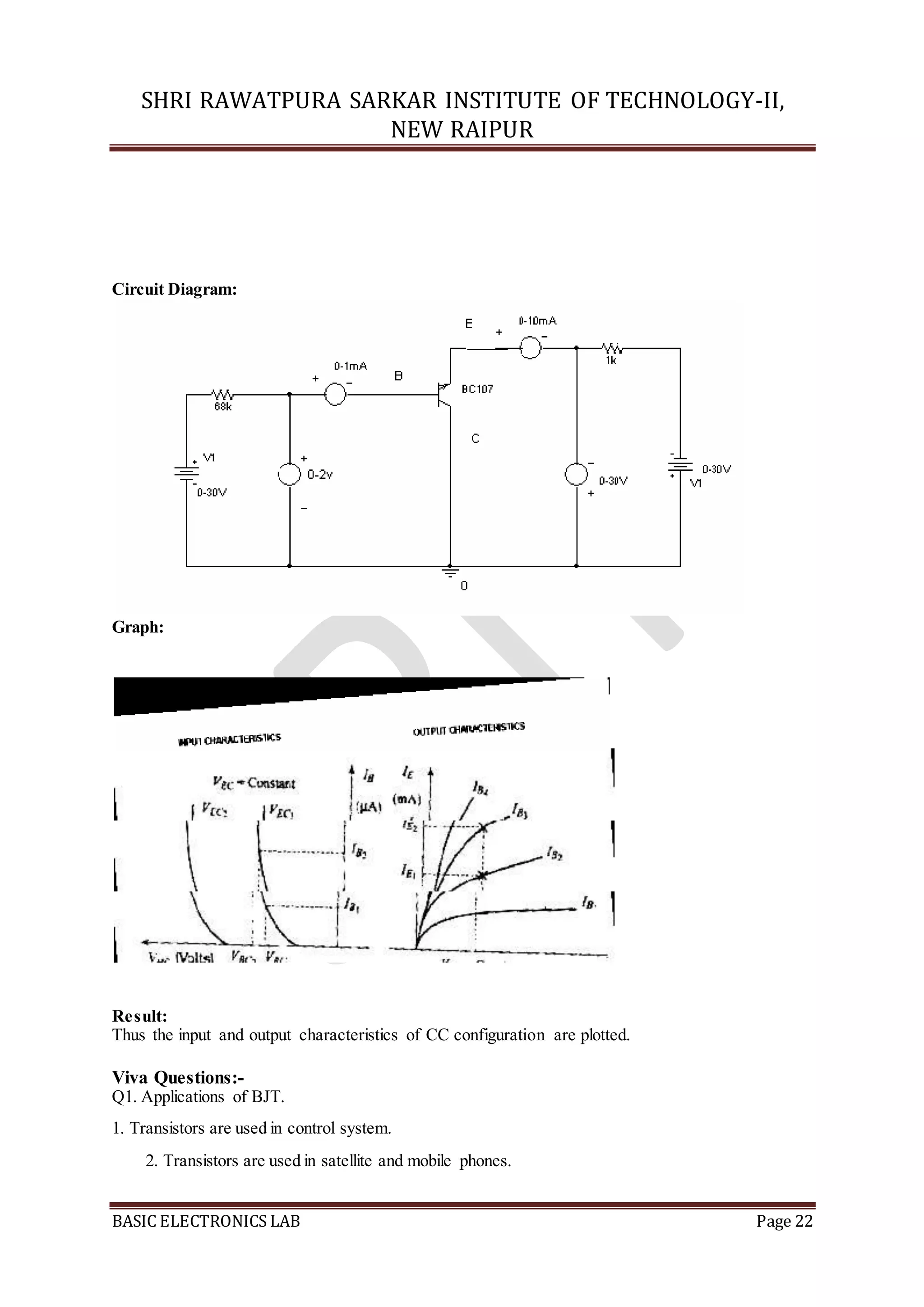
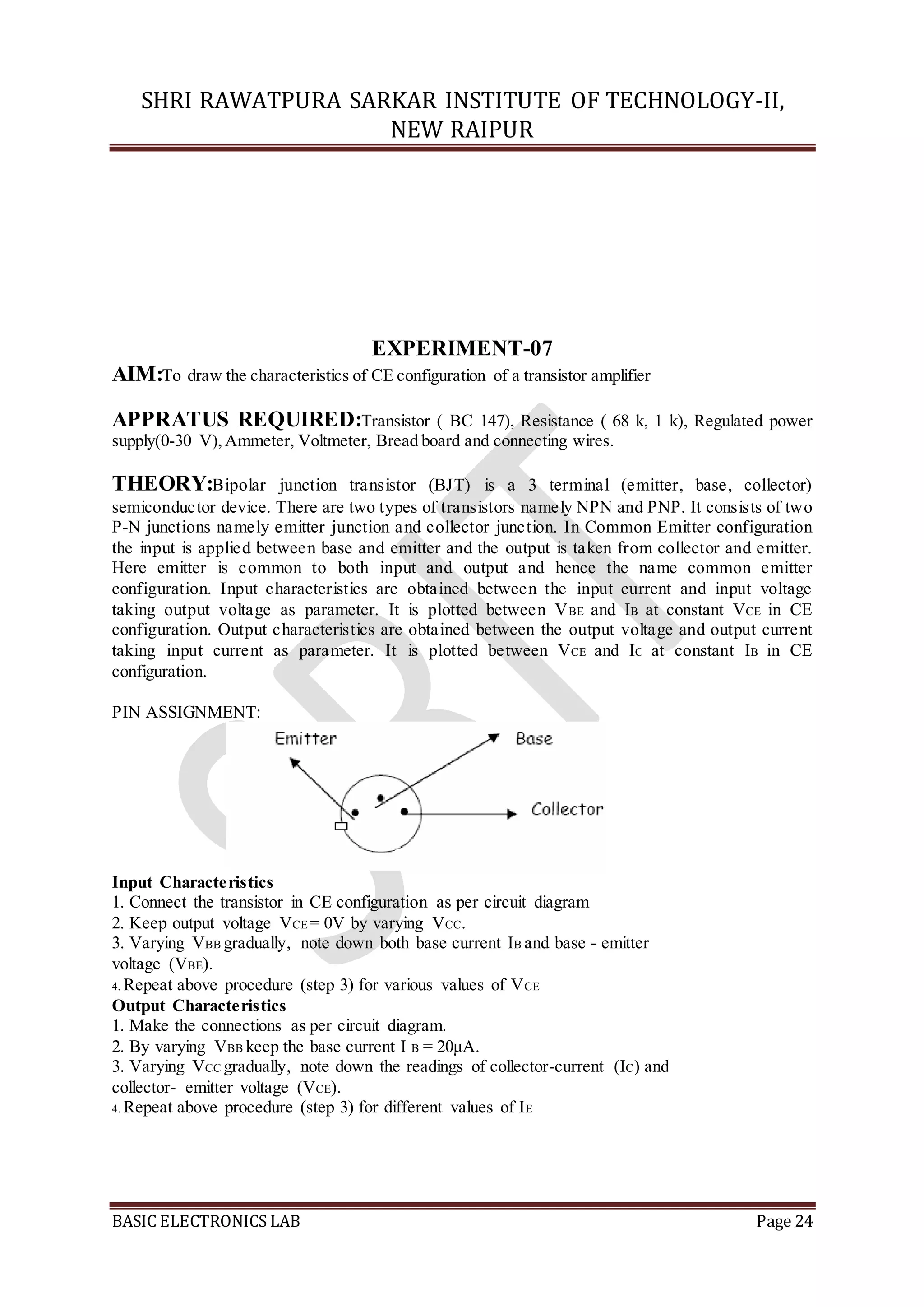
Download to read offline

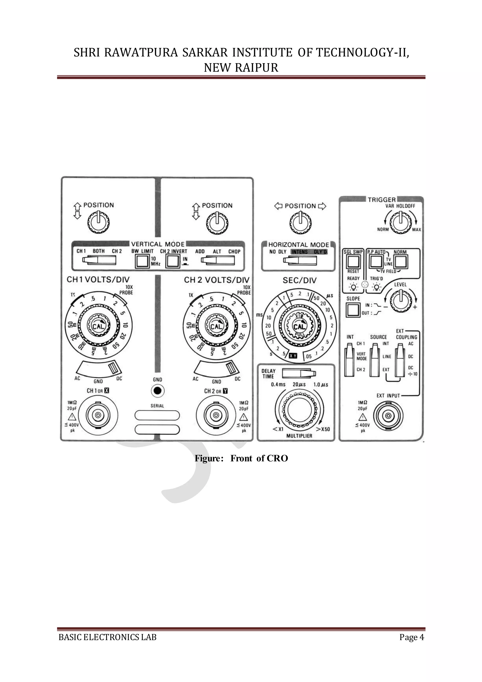
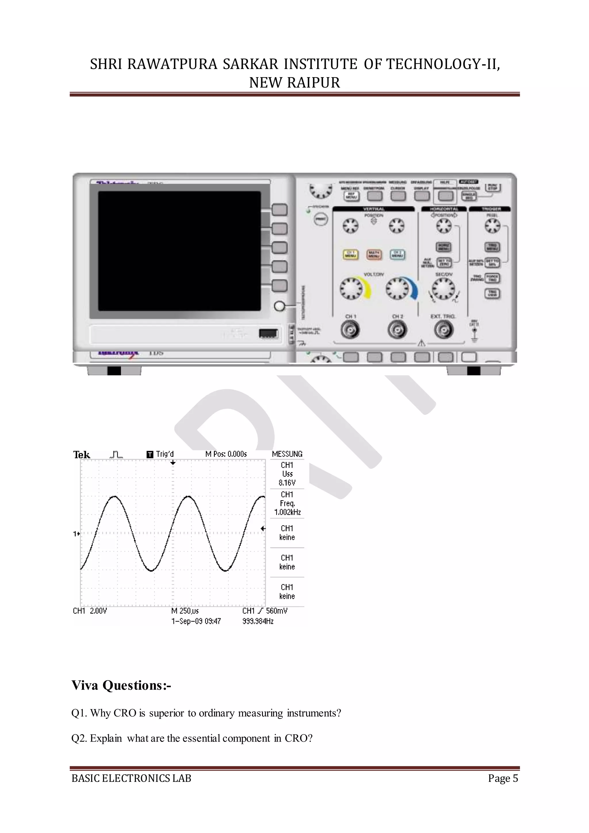


The document outlines a series of experiments conducted in a basic electronics lab at Shri Rawatpura Sarkar Institute of Technology-II, Raipur, focusing on the operation of cathode ray oscilloscopes (CRO) and digital storage oscilloscopes (DSO), along with semiconductor diode characteristics. It includes detailed procedures and theories related to various experiments such as diode characteristics, Zener diode behavior, and rectifier design, aimed at understanding essential electronic components and their applications. Key topics include oscilloscope functions, diode forward and reverse bias characteristics, and rectification processes, supported by viva questions for assessment.