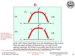
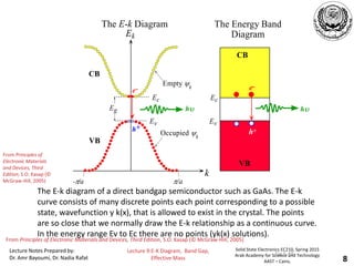
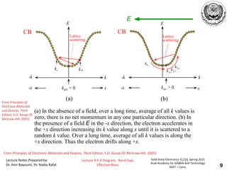
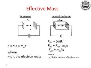
This document contains lecture notes on band theory, E-K diagrams, energy gaps, and effective mass in solid state electronics. It includes diagrams and explanations of how the energy-momentum (E-K) diagram represents allowed electron states in crystals and how energy gaps differentiate metals, semiconductors and insulators. It also discusses how the effective mass of electrons inside crystals is different than in vacuum due to interactions with the lattice, and how this affects electron acceleration under an applied electric field.

![Lecture Notes Prepared by:
Dr. Amr Bayoumi, Dr. Nadia Rafat
Solid State Electronics EC210, Spring 2015
Arab Academy for Science and Technology
AAST – Cairo,
Lecture 9:E-K Diagram, Band Gap,
Effective Mass 5
From Principles of Electronic Materials and Devices, Third Edition, S.O. Kasap (© McGraw-Hill, 2005)
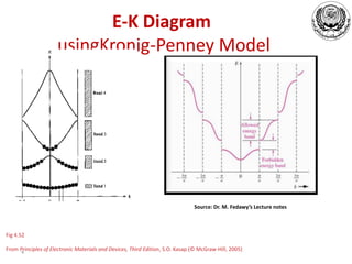
Energy Gap (Bandgaps, Eg)
Fig 4.54
a
E
[11]
k3
E
k1
[10]
Band
Band
Energy gap
Energy gap
Band
Band
First
Brillouin Zone
Second Brillouin
Zone
Second
Brillouin Zone
First
Brillouin Zone
a
The E-k behavior for the electron along different directions in the two
dimensional crystal. The energy gap along [10] is at /a whereas it is
at /a along [11].
From Principles of
Electronic Materials
and Devices, Third
Edition, S.O. Kasap (©
McGraw-Hill, 2005)](https://image.slidesharecdn.com/35230875ec2102015121lect9-e-k-eg-meff-sp15-230521042652-f20c0872/85/BAND-THEORY-pdf-5-320.jpg)
![Lecture Notes Prepared by:
Dr. Amr Bayoumi, Dr. Nadia Rafat
Solid State Electronics EC210, Spring 2015
Arab Academy for Science and Technology
AAST – Cairo,
Lecture 9:E-K Diagram, Band Gap,
Effective Mass 6
From Principles of Electronic Materials and Devices, Third Edition, S.O. Kasap (© McGraw-Hill, 2005)
Energy Gaps (Eg)
Fig 4.55
(a) Metal: For the electron in a metal there is no apparent energy gap
because the 2nd BZ (Brillouin Zone) along [10] overlaps the 1st BZ along
[11]. Bands overlap the energy gaps. Thus the electron can always find any
energy by changing its direction.
(b) Semiconductor or insulator: For the electron in a semiconductor there is
an energy gap arising from the overlap of the energy gaps along [10] and
[11] directions. The electron can never have an energy within this energy
gap, Eg.
Energy gap
[11]
[10] Overlapped
energy gaps
Energy gap = Eg
1st BZ
band
2nd BZ
band
(b) Semiconductor and insulator
Energy gap
[11]
[10]
Bands overlap
energy gaps
Energy gap
1st BZ
band
2nd BZ
&
1st BZ
overlapped
band
2nd BZ
band
(a) Metal
From Principles of
Electronic Materials
and Devices, Third
Edition, S.O. Kasap (©
McGraw-Hill, 2005)](https://image.slidesharecdn.com/35230875ec2102015121lect9-e-k-eg-meff-sp15-230521042652-f20c0872/85/BAND-THEORY-pdf-6-320.jpg)