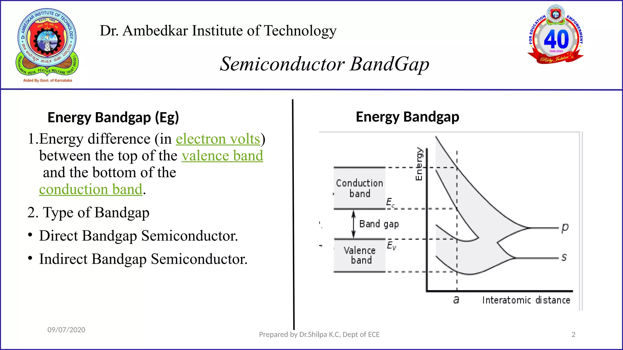
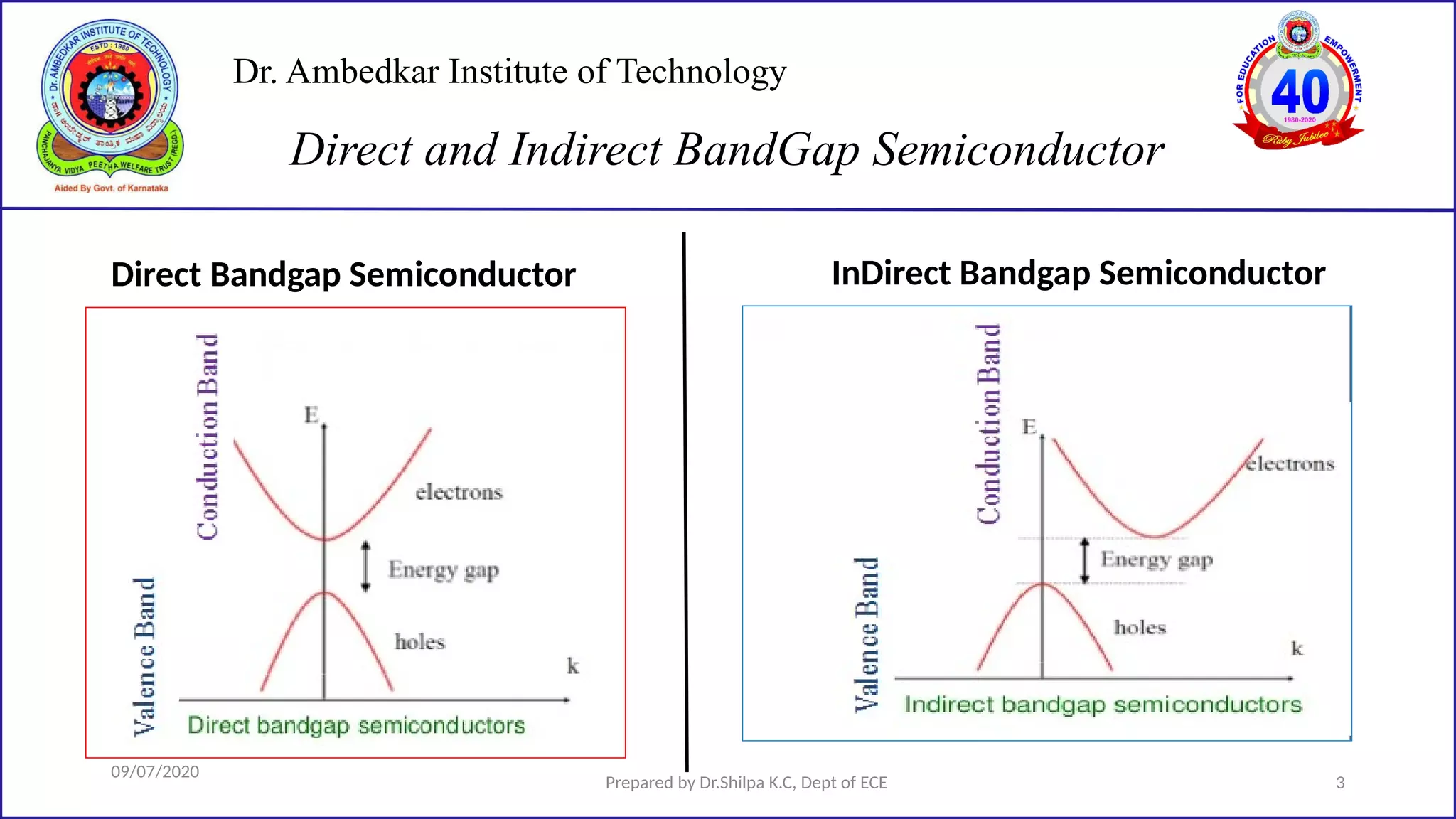
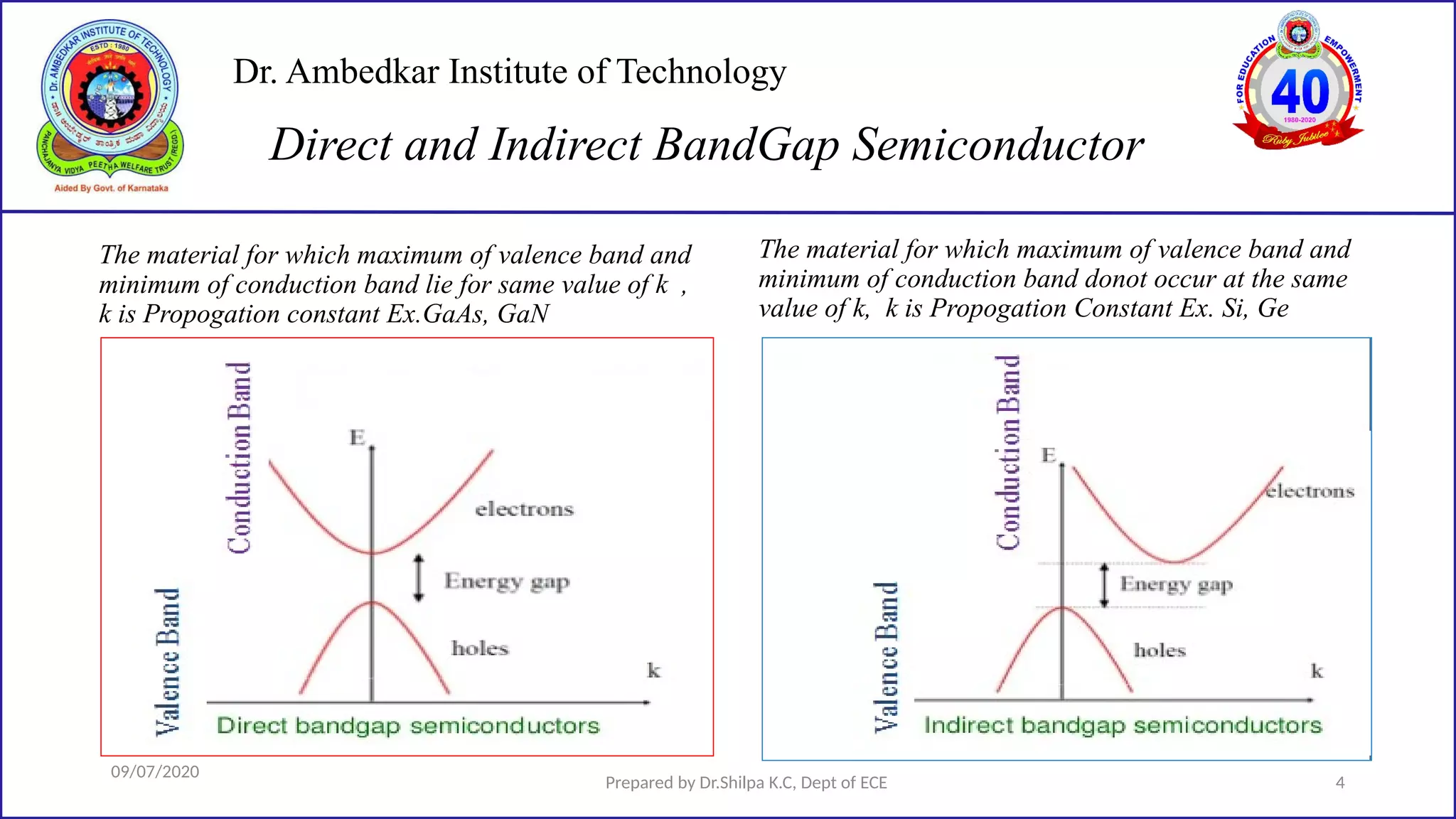
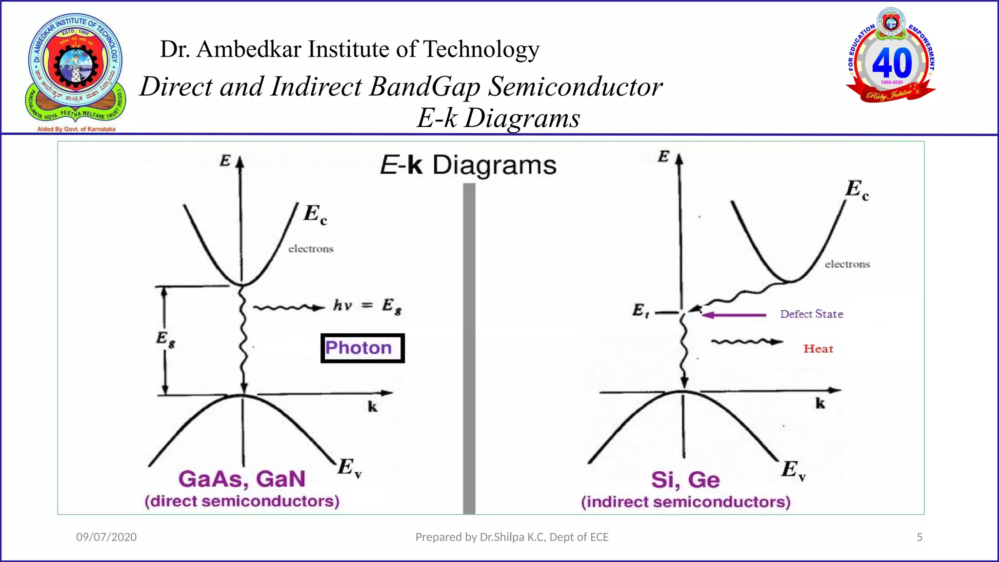
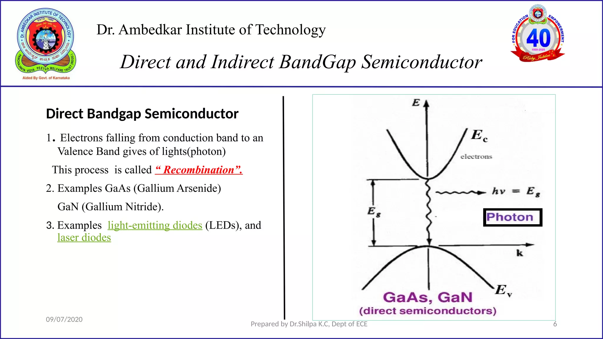
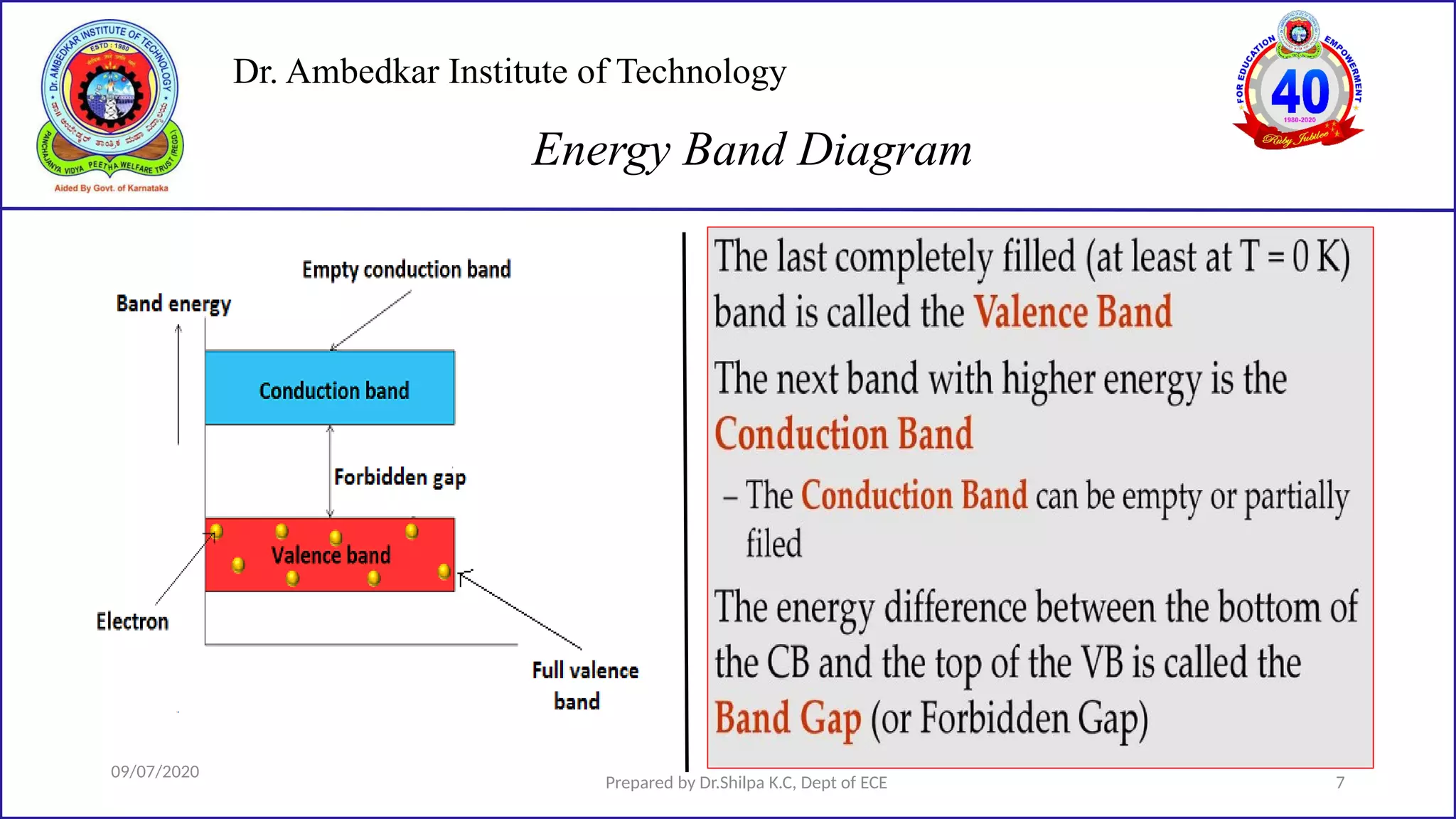
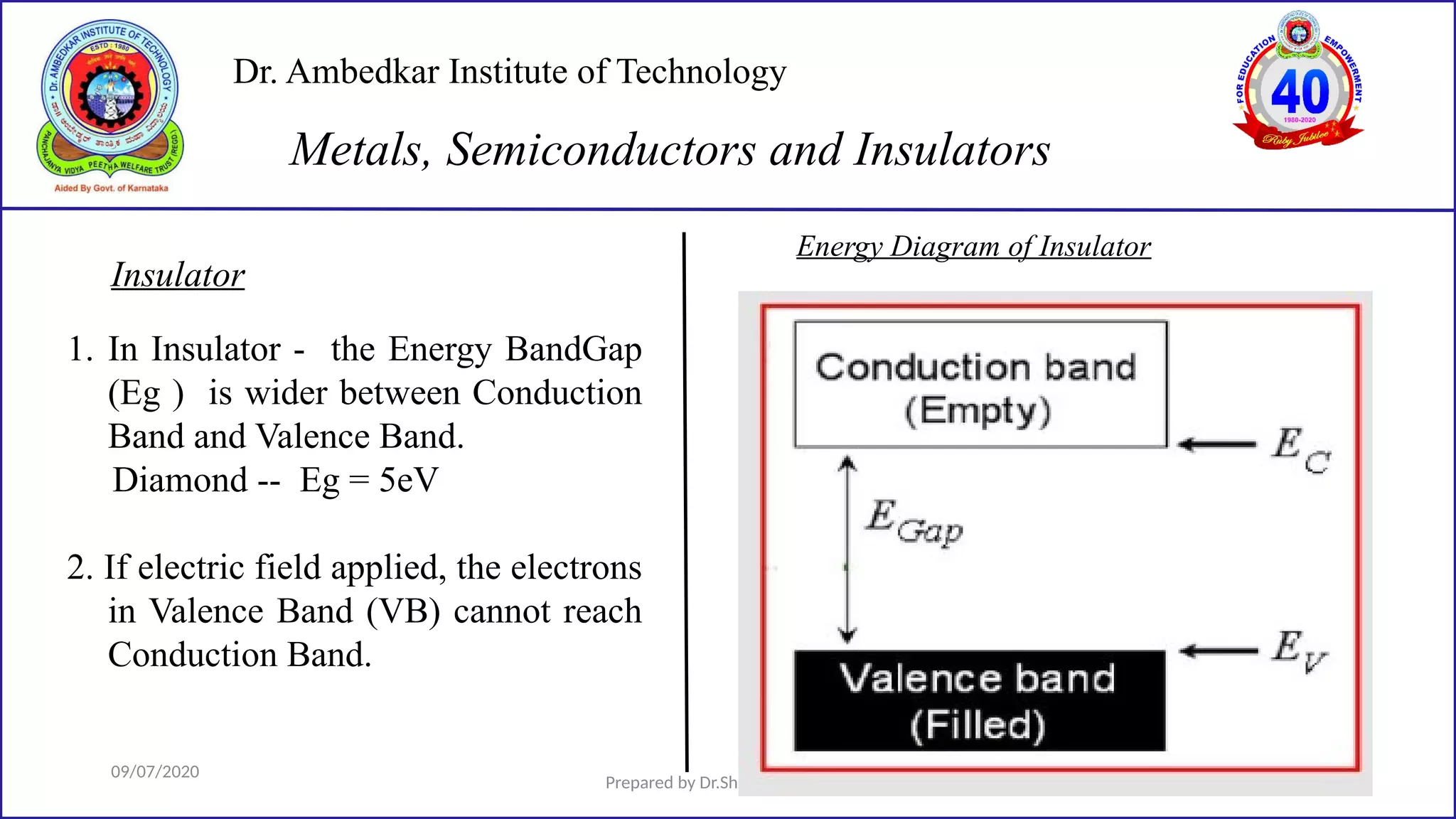
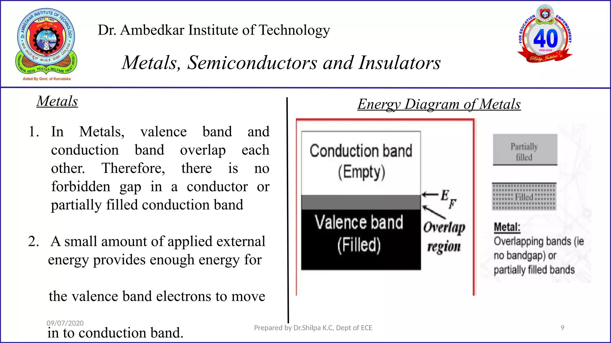
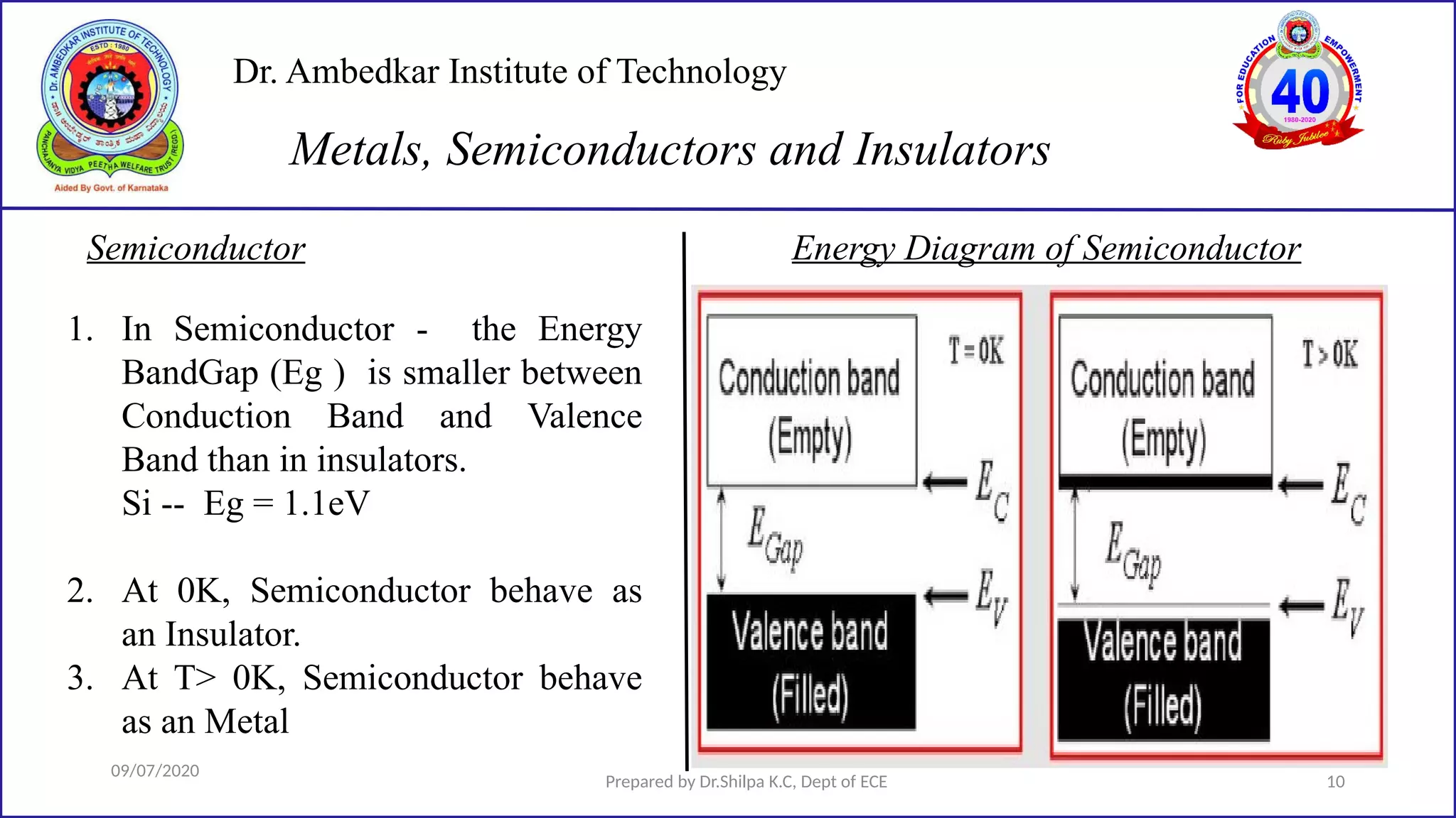
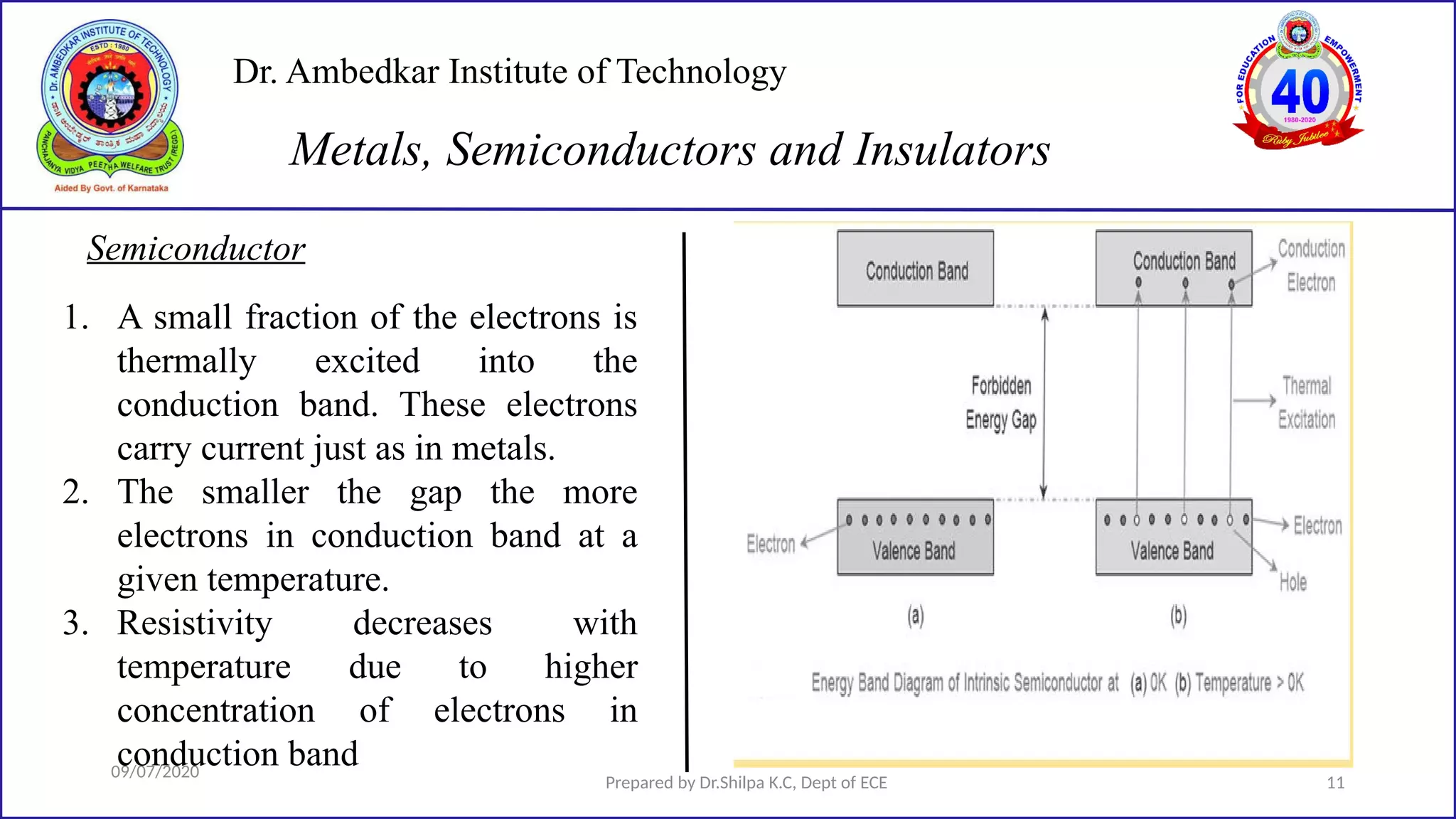
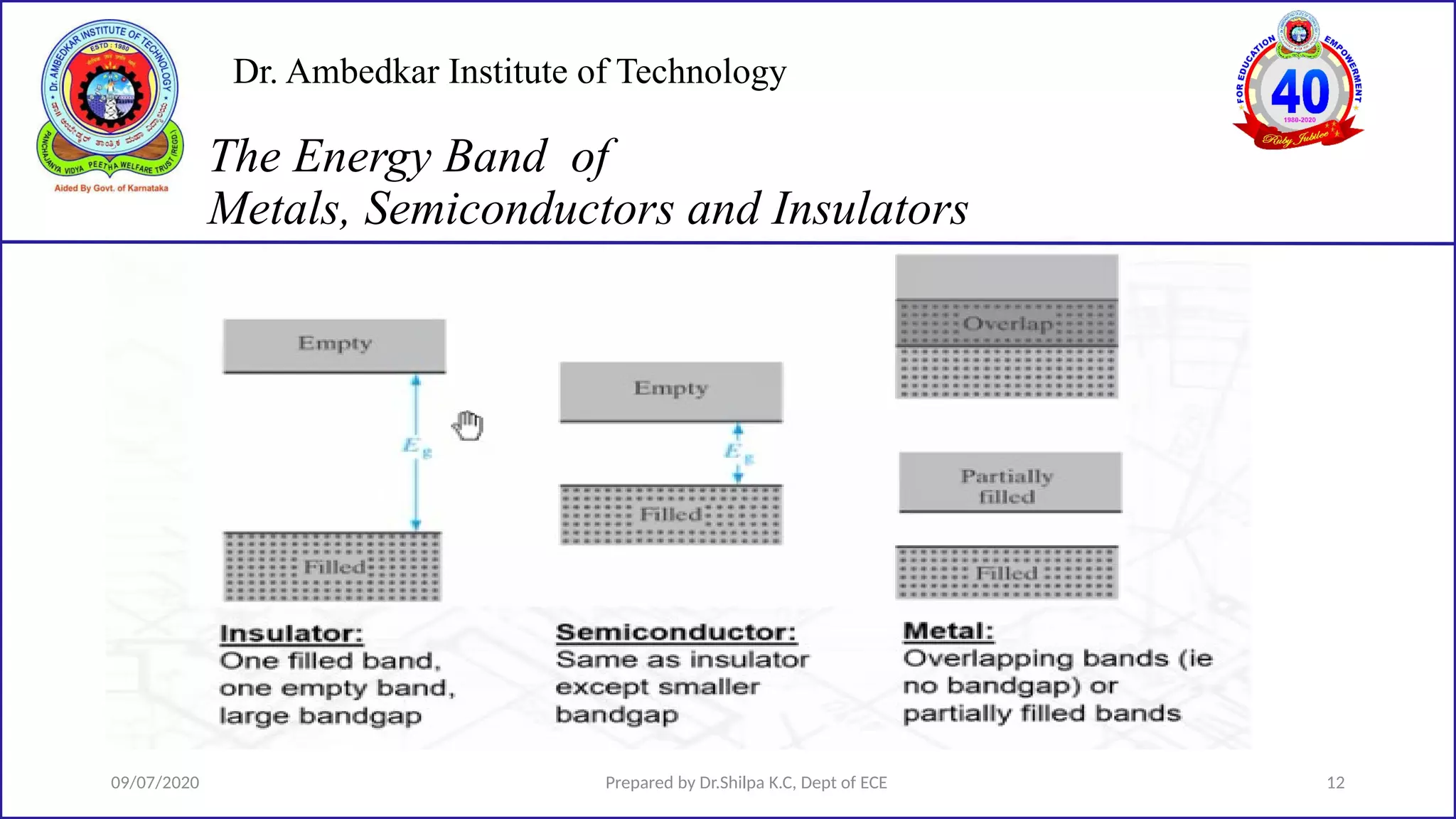
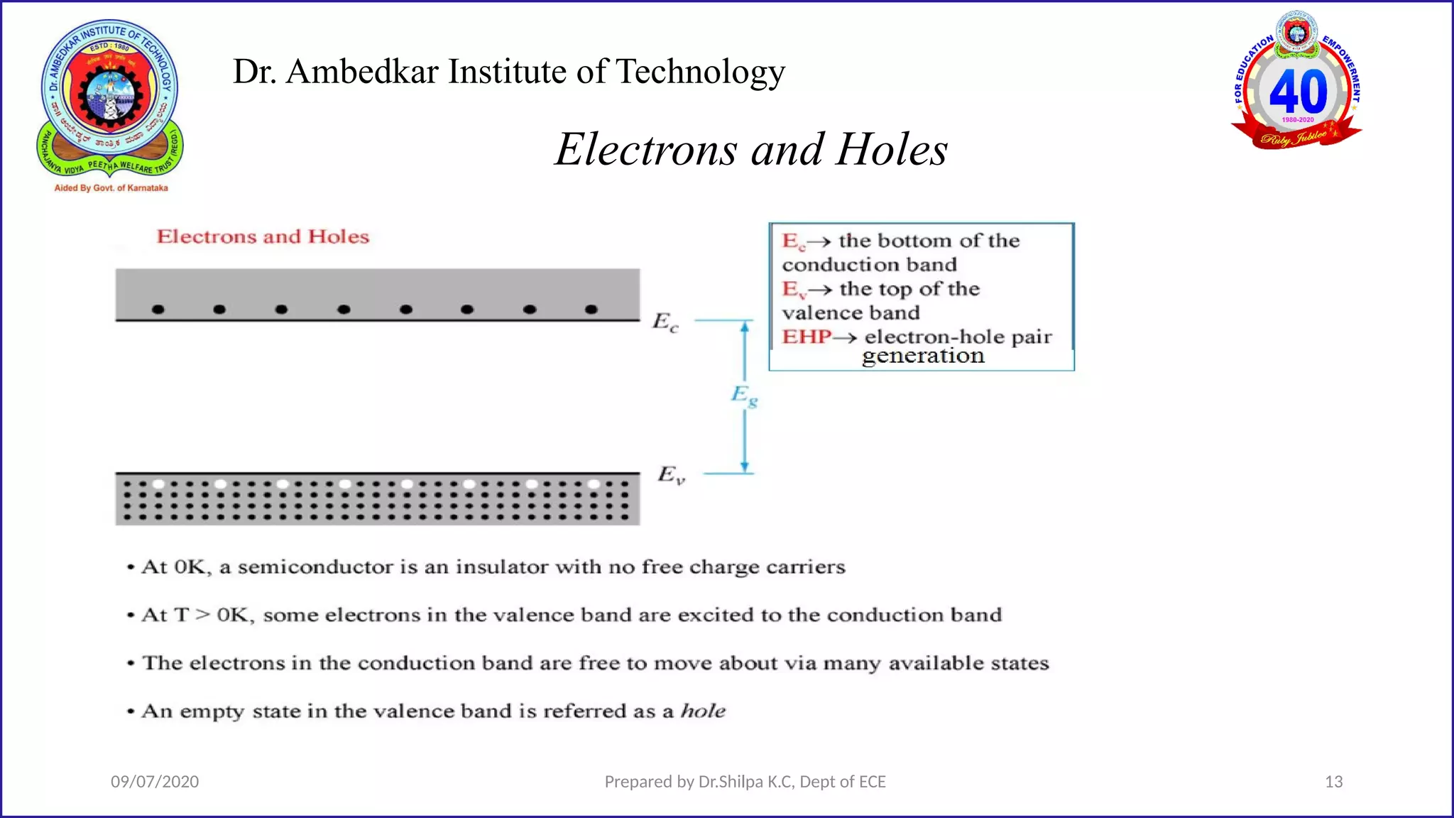
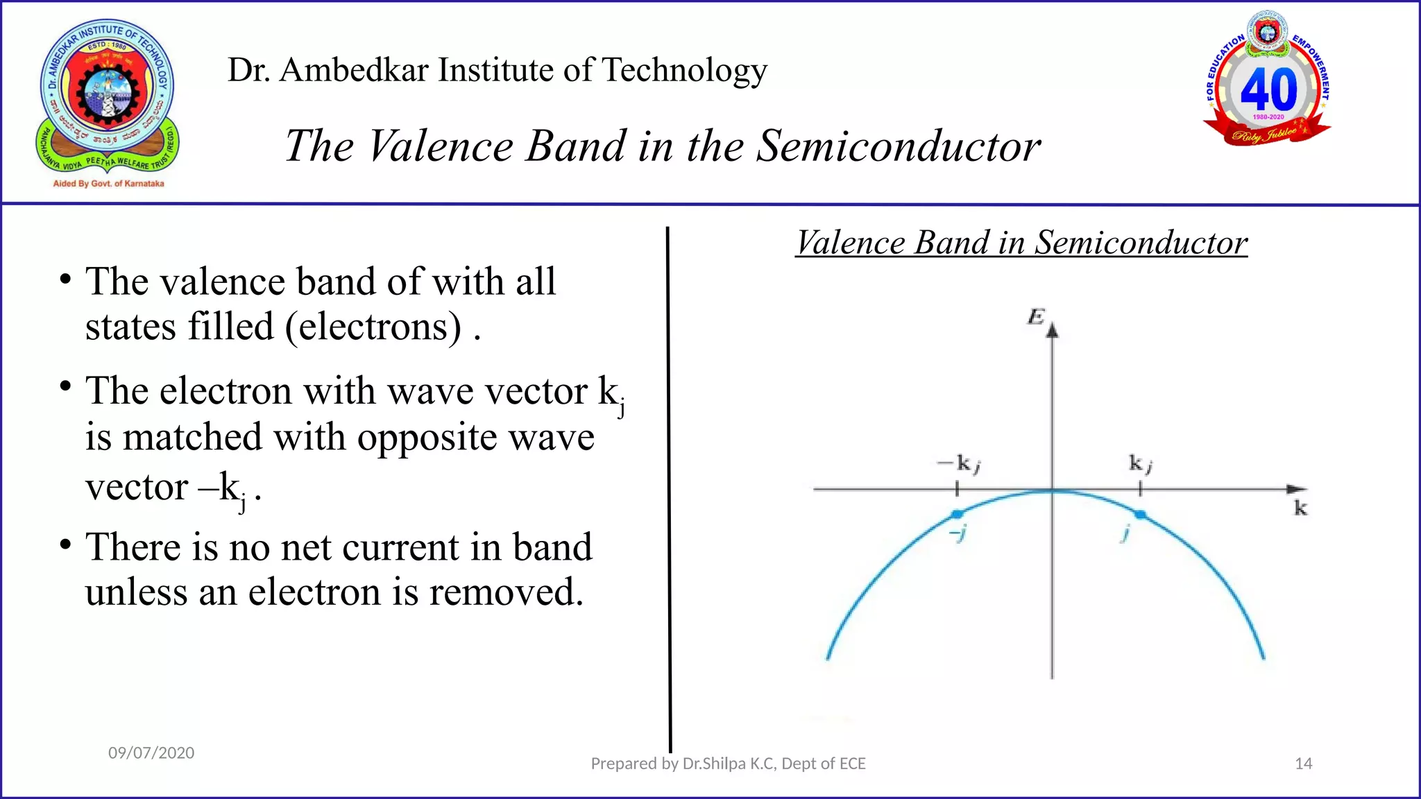
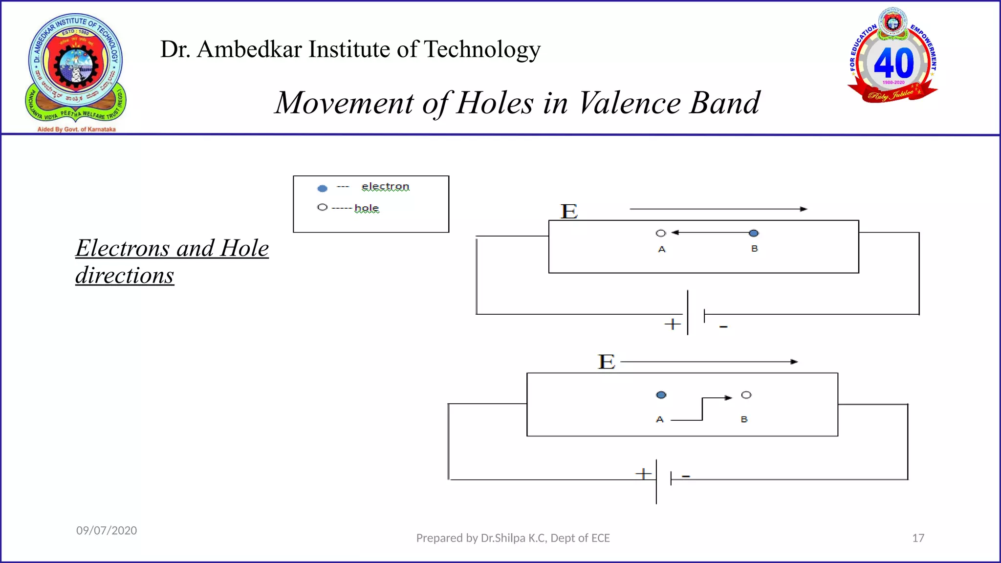
Dr. Ambedkar Institute of Technology
Electronics Devices (19EC31)
Class 4
Dr. Ambedkar Institute of
Technology
Dr. Shilpa K.C
Assistant
Professor
Dept. of
Electronics and
Communication
Engineering
Dr.AIT
09/07/2020 1
Prepared by Dr.Shilpa K.C, Dept of ECE
Dr. Ambedkar Institute of Technology
Energy Bandgap (Eg) Energy Bandgap
09/07/2020
Prepared by Dr.Shilpa K.C, Dept of ECE 2
Semiconductor BandGap
1.Energy difference (in electron volts)
between the top of the valence band
and the bottom of the
conduction band.
2. Type of Bandgap
• Direct Bandgap Semiconductor.
• Indirect Bandgap Semiconductor.
Dr. Ambedkar Institute of Technology
Direct Bandgap Semiconductor InDirect Bandgap Semiconductor
09/07/2020
Prepared by Dr.Shilpa K.C, Dept of ECE 3
Direct and Indirect BandGap Semiconductor
Dr. Ambedkar Institute of Technology
Direct and Indirect BandGap Semiconductor
09/07/2020
Prepared by Dr.Shilpa K.C, Dept of ECE 4
The material for which maximum of valence band and
minimum of conduction band donot occur at the same
value of k, k is Propogation Constant Ex. Si, Ge
The material for which maximum of valence band and
minimum of conduction band lie for same value of k ,
k is Propogation constant Ex.GaAs, GaN
Dr. Ambedkar Institute of Technology
09/07/2020 Prepared by Dr.Shilpa K.C, Dept of ECE 5
Direct and Indirect BandGap Semiconductor
E-k Diagrams
Dr. Ambedkar Institute of Technology
Direct Bandgap Semiconductor
09/07/2020
Prepared by Dr.Shilpa K.C, Dept of ECE 6
Direct and Indirect BandGap Semiconductor
1. Electrons falling from conduction band to an
Valence Band gives of lights(photon)
This process is called “ Recombination”.
2. Examples GaAs (Gallium Arsenide)
GaN (Gallium Nitride).
3. Examples light-emitting diodes (LEDs), and
laser diodes
Dr. Ambedkar Institute of Technology
09/07/2020
Prepared by Dr.Shilpa K.C, Dept of ECE 7
Energy Band Diagram
Dr. Ambedkar Institute of Technology
Insulator
09/07/2020
Prepared by Dr.Shilpa K.C, Dept of ECE 8
Metals, Semiconductors and Insulators
1. In Insulator - the Energy BandGap
(Eg ) is wider between Conduction
Band and Valence Band.
Diamond -- Eg = 5eV
2. If electric field applied, the electrons
in Valence Band (VB) cannot reach
Conduction Band.
Energy Diagram of Insulator
Dr. Ambedkar Institute of Technology
Metals
09/07/2020
Prepared by Dr.Shilpa K.C, Dept of ECE 9
Metals, Semiconductors and Insulators
Energy Diagram of Metals
1. In Metals, valence band and
conduction band overlap each
other. Therefore, there is no
forbidden gap in a conductor or
partially filled conduction band
2. A small amount of applied external
energy provides enough energy for
the valence band electrons to move
in to conduction band.
Dr. Ambedkar Institute of Technology
Semiconductor
09/07/2020
Prepared by Dr.Shilpa K.C, Dept of ECE 10
Metals, Semiconductors and Insulators
Energy Diagram of Semiconductor
1. In Semiconductor - the Energy
BandGap (Eg ) is smaller between
Conduction Band and Valence
Band than in insulators.
Si -- Eg = 1.1eV
2. At 0K, Semiconductor behave as
an Insulator.
3. At T> 0K, Semiconductor behave
as an Metal
Dr. Ambedkar Institute of Technology
Semiconductor
09/07/2020
Prepared by Dr.Shilpa K.C, Dept of ECE 11
Metals, Semiconductors and Insulators
Energy Diagram of Semiconductor
1. A small fraction of the electrons is
thermally excited into the
conduction band. These electrons
carry current just as in metals.
2. The smaller the gap the more
electrons in conduction band at a
given temperature.
3. Resistivity decreases with
temperature due to higher
concentration of electrons in
conduction band
Dr. Ambedkar Institute of Technology
09/07/2020 Prepared by Dr.Shilpa K.C, Dept of ECE 12
The Energy Band of
Metals, Semiconductors and Insulators
Dr. Ambedkar Institute of Technology
09/07/2020 Prepared by Dr.Shilpa K.C, Dept of ECE 13
Electrons and Holes
Dr. Ambedkar Institute of Technology
09/07/2020
Prepared by Dr.Shilpa K.C, Dept of ECE 14
The Valence Band in the Semiconductor
Valence Band in Semiconductor
• The valence band of with all
states filled (electrons) .
• The electron with wave vector kj
is matched with opposite wave
vector –kj .
• There is no net current in band
unless an electron is removed.
Dr. Ambedkar Institute of Technology
09/07/2020
Prepared by Dr.Shilpa K.C, Dept of ECE 15
The concept of Hole
Dr. Ambedkar Institute of Technology
09/07/2020
Prepared by Dr.Shilpa K.C, Dept of ECE 16
Mechanism of Hole movement
Hole Movement
Dr. Ambedkar Institute of Technology
09/07/2020
Prepared by Dr.Shilpa K.C, Dept of ECE 17
Movement of Holes in Valence Band
Electrons and Hole
directions
Dr. Ambedkar Institute of Technology
Thank You
Dr. Ambedkar
Institute of Technology
HAVE A NICE DAY
09/07/2020 18
Prepared by Dr.Shilpa K.C, Dept of ECE

Electronics_Devices_class_4.pdf

  • 1.
    Dr. Ambedkar Instituteof Technology Electronics Devices (19EC31) Class 4 Dr. Ambedkar Institute of Technology Dr. Shilpa K.C Assistant Professor Dept. of Electronics and Communication Engineering Dr.AIT 09/07/2020 1 Prepared by Dr.Shilpa K.C, Dept of ECE
  • 2.
    Dr. Ambedkar Instituteof Technology Energy Bandgap (Eg) Energy Bandgap 09/07/2020 Prepared by Dr.Shilpa K.C, Dept of ECE 2 Semiconductor BandGap 1.Energy difference (in electron volts) between the top of the valence band and the bottom of the conduction band. 2. Type of Bandgap • Direct Bandgap Semiconductor. • Indirect Bandgap Semiconductor.
  • 3.
    Dr. Ambedkar Instituteof Technology Direct Bandgap Semiconductor InDirect Bandgap Semiconductor 09/07/2020 Prepared by Dr.Shilpa K.C, Dept of ECE 3 Direct and Indirect BandGap Semiconductor
  • 4.
    Dr. Ambedkar Instituteof Technology Direct and Indirect BandGap Semiconductor 09/07/2020 Prepared by Dr.Shilpa K.C, Dept of ECE 4 The material for which maximum of valence band and minimum of conduction band donot occur at the same value of k, k is Propogation Constant Ex. Si, Ge The material for which maximum of valence band and minimum of conduction band lie for same value of k , k is Propogation constant Ex.GaAs, GaN
  • 5.
    Dr. Ambedkar Instituteof Technology 09/07/2020 Prepared by Dr.Shilpa K.C, Dept of ECE 5 Direct and Indirect BandGap Semiconductor E-k Diagrams
  • 6.
    Dr. Ambedkar Instituteof Technology Direct Bandgap Semiconductor 09/07/2020 Prepared by Dr.Shilpa K.C, Dept of ECE 6 Direct and Indirect BandGap Semiconductor 1. Electrons falling from conduction band to an Valence Band gives of lights(photon) This process is called “ Recombination”. 2. Examples GaAs (Gallium Arsenide) GaN (Gallium Nitride). 3. Examples light-emitting diodes (LEDs), and laser diodes
  • 7.
    Dr. Ambedkar Instituteof Technology 09/07/2020 Prepared by Dr.Shilpa K.C, Dept of ECE 7 Energy Band Diagram
  • 8.
    Dr. Ambedkar Instituteof Technology Insulator 09/07/2020 Prepared by Dr.Shilpa K.C, Dept of ECE 8 Metals, Semiconductors and Insulators 1. In Insulator - the Energy BandGap (Eg ) is wider between Conduction Band and Valence Band. Diamond -- Eg = 5eV 2. If electric field applied, the electrons in Valence Band (VB) cannot reach Conduction Band. Energy Diagram of Insulator
  • 9.
    Dr. Ambedkar Instituteof Technology Metals 09/07/2020 Prepared by Dr.Shilpa K.C, Dept of ECE 9 Metals, Semiconductors and Insulators Energy Diagram of Metals 1. In Metals, valence band and conduction band overlap each other. Therefore, there is no forbidden gap in a conductor or partially filled conduction band 2. A small amount of applied external energy provides enough energy for the valence band electrons to move in to conduction band.
  • 10.
    Dr. Ambedkar Instituteof Technology Semiconductor 09/07/2020 Prepared by Dr.Shilpa K.C, Dept of ECE 10 Metals, Semiconductors and Insulators Energy Diagram of Semiconductor 1. In Semiconductor - the Energy BandGap (Eg ) is smaller between Conduction Band and Valence Band than in insulators. Si -- Eg = 1.1eV 2. At 0K, Semiconductor behave as an Insulator. 3. At T> 0K, Semiconductor behave as an Metal
  • 11.
    Dr. Ambedkar Instituteof Technology Semiconductor 09/07/2020 Prepared by Dr.Shilpa K.C, Dept of ECE 11 Metals, Semiconductors and Insulators Energy Diagram of Semiconductor 1. A small fraction of the electrons is thermally excited into the conduction band. These electrons carry current just as in metals. 2. The smaller the gap the more electrons in conduction band at a given temperature. 3. Resistivity decreases with temperature due to higher concentration of electrons in conduction band
  • 12.
    Dr. Ambedkar Instituteof Technology 09/07/2020 Prepared by Dr.Shilpa K.C, Dept of ECE 12 The Energy Band of Metals, Semiconductors and Insulators
  • 13.
    Dr. Ambedkar Instituteof Technology 09/07/2020 Prepared by Dr.Shilpa K.C, Dept of ECE 13 Electrons and Holes
  • 14.
    Dr. Ambedkar Instituteof Technology 09/07/2020 Prepared by Dr.Shilpa K.C, Dept of ECE 14 The Valence Band in the Semiconductor Valence Band in Semiconductor • The valence band of with all states filled (electrons) . • The electron with wave vector kj is matched with opposite wave vector –kj . • There is no net current in band unless an electron is removed.
  • 15.
    Dr. Ambedkar Instituteof Technology 09/07/2020 Prepared by Dr.Shilpa K.C, Dept of ECE 15 The concept of Hole
  • 16.
    Dr. Ambedkar Instituteof Technology 09/07/2020 Prepared by Dr.Shilpa K.C, Dept of ECE 16 Mechanism of Hole movement Hole Movement
  • 17.
    Dr. Ambedkar Instituteof Technology 09/07/2020 Prepared by Dr.Shilpa K.C, Dept of ECE 17 Movement of Holes in Valence Band Electrons and Hole directions
  • 18.
    Dr. Ambedkar Instituteof Technology Thank You Dr. Ambedkar Institute of Technology HAVE A NICE DAY 09/07/2020 18 Prepared by Dr.Shilpa K.C, Dept of ECE