Advanced VLSI Design:2023-24
Lecture 5
Static Timing Analysis
ELECTRICAL ELECTRONICS COMMUNICATION INSTRUMENTATION
By Dr. Sanjay Vidhyadharan
2.
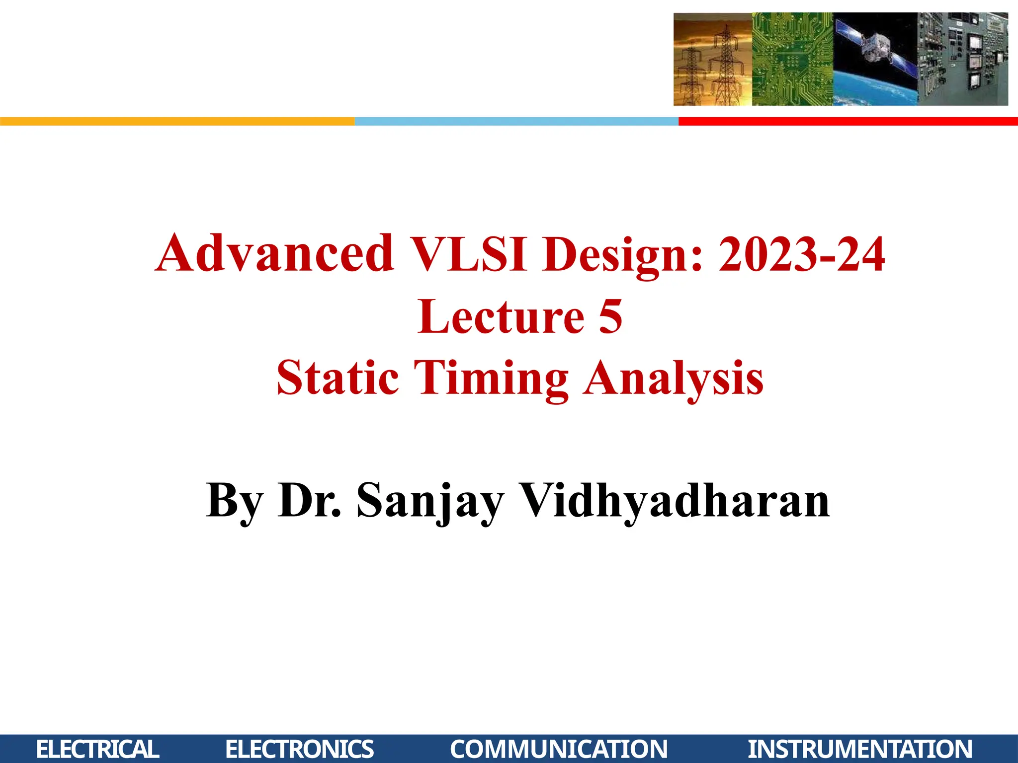
Timing Constraints ofa Flip-flop
8/19/2023
ELECTRICAL
2
INSTRUMENTATIO
ELECTRONICS COMMUNICATION
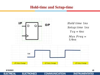
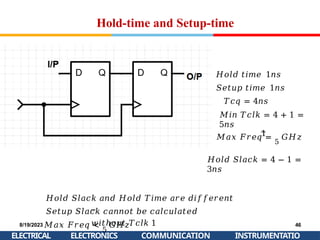
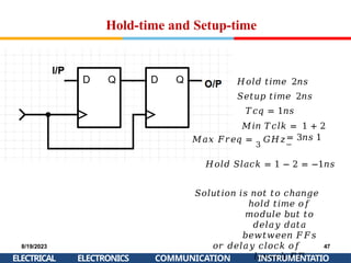
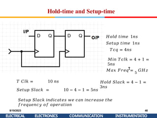
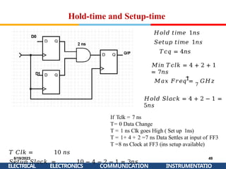
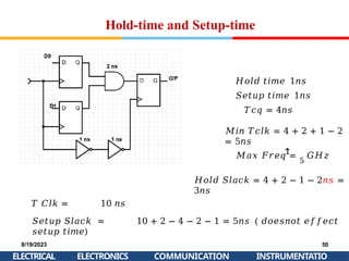
Setup Time
Hold Time
3.
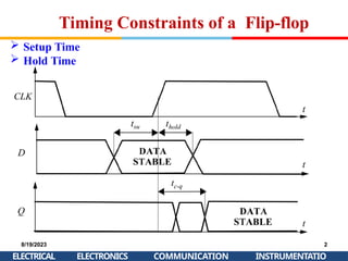
Clock Skew andJitter
8/19/2023
ELECTRICAL
3
INSTRUMENTATIO
ELECTRONICS COMMUNICATION
Clock skew (sometimes called timing skew) is a phenomenon in synchronous digital
circuit systems (such as computer systems) in which the same sourced clock signal arrives
at different components at different times. Cause : Wires , Buffers etc
Clock Jitter: Sometimes some external sources like noise, voltage variations may cause
to disrupt the natural periodicity or frequency of the clock. This deviation from the natural
location of the clock is termed to be clock jitter.
Clock Uncertainty = Clock Jitter + Clock Skew
4.
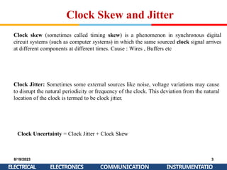
Timing Constraints ofa Flip-flop
Data setup violation caused by clock uncertainty
8/19/2023
ELECTRICAL
4
INSTRUMENTATIO
ELECTRONICS COMMUNICATION
5.
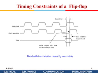
Timing Constraints ofa Flip-flop
Data hold time violation caused by uncertainty
8/19/2023
ELECTRICAL
5
INSTRUMENTATIO
ELECTRONICS COMMUNICATION
6.
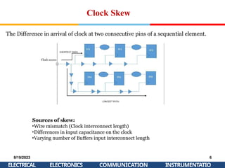
Clock Skew
The Differencein arrival of clock at two consecutive pins of a sequential element.
Sources of skew:
•Wire mismatch (Clock interconnect length)
•Differences in input capacitance on the clock
•Varying number of Buffers input interconnect length
8/19/2023
ELECTRICAL
6
INSTRUMENTATIO
ELECTRONICS COMMUNICATION
7.
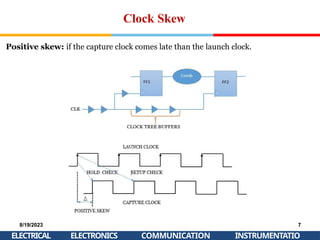
Clock Skew
Positive skew:if the capture clock comes late than the launch clock.
8/19/2023
ELECTRICAL
7
INSTRUMENTATIO
ELECTRONICS COMMUNICATION
8.
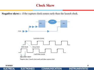
Clock Skew
Negative skew:: if the capture clock comes early than the launch clock.
8/19/2023
ELECTRICAL
8
INSTRUMENTATIO
ELECTRONICS COMMUNICATION
9.
Static Time Analysis
8/19/2023
ELECTRICAL
9
INSTRUMENTATIO
ELECTRONICSCOMMUNICATION
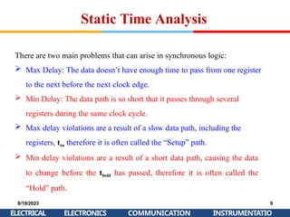
There are two main problems that can arise in synchronous logic:
Max Delay: The data doesn’t have enough time to pass from one register
to the next before the next clock edge.
Min Delay: The data path is so short that it passes through several
registers during the same clock cycle.
Max delay violations are a result of a slow data path, including the
registers, tsu therefore it is often called the “Setup” path.
Min delay violations are a result of a short data path, causing the data
to change before the thold has passed, therefore it is often called the
“Hold” path.
10.
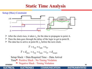
Static Time Analysis
Setup(Max) Constraint
After the clock rises, it takes tcq for the data to propagate to point A.
Then the data goes through the delay of the logic to get to point B.
The data has to arrive at point B, tsu before the next clock.
Setup Slack = Data Required Time – Data Arrival
Time
Positive Slack : No Timing Violation
Negative Slack : Timing Violation
8/19/2023
ELECTRICAL
10
INSTRUMENTATIO
ELECTRONICS COMMUNICATION
11.
Static Time Analysis
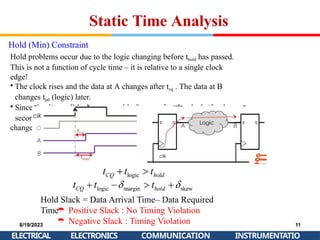
Hold(Min) Constraint
Hold problems occur due to the logic changing before thold has passed.
This is not a function of cycle time – it is relative to a single clock
edge!
• The clock rises and the data at A changes after tcq . The data at B
changes tpd (logic) later.
• Since the data at B had to stay stable for thold after the clock (for the
second register), the
change at B has to be at least thold after the clock edge.
Hold Slack = Data Arrival Time– Data Required
Time
Positive Slack : No Timing Violation
Negative Slack : Timing Violation
8/19/2023
ELECTRICAL
11
INSTRUMENTATIO
ELECTRONICS COMMUNICATION
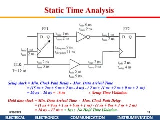
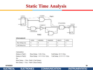
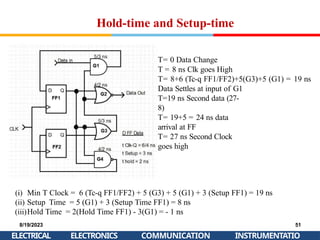
8/19/2023 13
= 18ns – 17 ns = + 1ns : No Hold Time Violation.
ELECTRICAL ELECTRONICS COMMUNICATION INSTRUMENTATION
T= 15 ns
Setup slack = Min. Clock Path Delay - Max. Data Arrival Time
= (15 ns + 2ns + 5 ns + 2 ns - 4 ns) - ( 2 ns + 11 ns +2 ns + 9 ns + 2 ns)
= 20 ns – 26 ns = -6 ns : Setup Time Violation.
Hold time slack = Min. Data Arrival Time - Max. Clock Path Delay
= (1 ns + 9 ns + 1 ns + 6 ns + 1 ns) - (3 ns + 9ns + 3 ns + 2 ns)
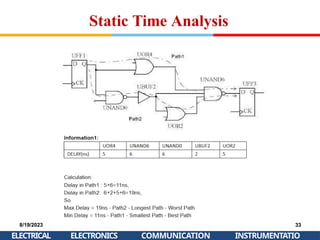
Static Time Analysis
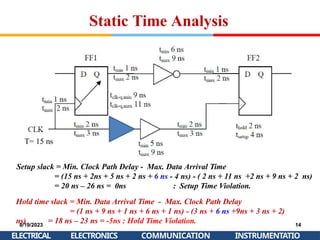
14.
T= 15 ns
Setupslack = Min. Clock Path Delay - Max. Data Arrival Time
= (15 ns + 2ns + 5 ns + 2 ns + 6 ns - 4 ns) - ( 2 ns + 11 ns +2 ns + 9 ns + 2 ns)
= 20 ns – 26 ns = 0ns : Setup Time Violation.
Hold time slack = Min. Data Arrival Time - Max. Clock Path Delay
= (1 ns + 9 ns + 1 ns + 6 ns + 1 ns) - (3 ns + 6 ns +9ns + 3 ns + 2)
ns) = 18 ns – 23 ns = -5ns : Hold Time Violation.
Static Time Analysis
8/19/2023
ELECTRICAL
14
INSTRUMENTATIO
ELECTRONICS COMMUNICATION
15.
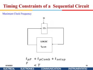
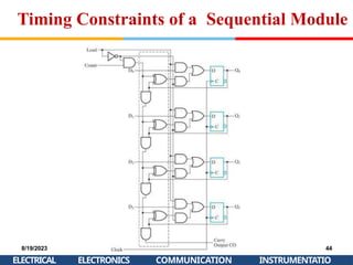
Timing Constraints ofa Sequential Circuit
Maximum Clock Frequency
𝑡𝑝𝐹
𝐹
8/19/2023
ELECTRICAL
15
INSTRUMENTATIO
ELECTRONICS COMMUNICATION
+ 𝑡𝑝𝐶𝑜𝑚𝑏 + 𝑡𝑠𝑒𝑡𝑢𝑝
< 𝑇
16.
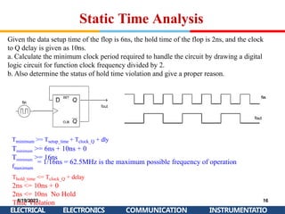
Static Time Analysis
Giventhe data setup time of the flop is 6ns, the hold time of the flop is 2ns, and the clock
to Q delay is given as 10ns.
a. Calculate the minimum clock period required to handle the circuit by drawing a digital
logic circuit for function clock frequency divided by 2.
b. Also determine the status of hold time violation and give a proper reason.
Tminimum >= Tsetup_time + Tclock_Q + dly
Tminimum >= 6ns + 10ns + 0
Tminimum >= 16ns
8/19/2023
ELECTRICAL
16
INSTRUMENTATIO
ELECTRONICS COMMUNICATION
fmaximum
= 1/16ns = 62.5MHz is the maximum possible frequency of operation
Thold_time <= Tclock_Q + delay
2ns <= 10ns + 0
2ns <= 10ns No Hold
Time Violation
17.
Static Time Analysis
8/19/2023
ELECTRICAL
17
INSTRUMENTATIO
ELECTRONICSCOMMUNICATION
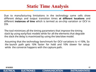
Due to manufacturing limitations in the technology same cells show
different delays and output transition times at different locations and
different instances of time which is termed as on-chip variation or OCV in
STA
The tool minimizes all the timing parameters that improve the timing
slack by using early/fast models while for all the elements that degrade
the slack the delay is maximized by using the late/slow model.
Assuming that the technology benchmark for OCV variations is +/-10%, So
the launch path gets 10% faster for hold and 10% slower for setup
while the converse happens with the capture path.
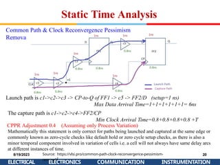
Static Time Analysis
CommonPath & Clock Reconvergence Pessimism
Removal
Launch path is c1->c2->c3 -> CP-to-Q of FF1 -> c5 -> FF2/D (setup=1 ns)
Source: https://vlsi.pro/common-path-clock-reconvergence-pessimism-
removal/
8/19/2023
ELECTRICAL
20
ELECTRONICS COMMUNICATION INSTRUMENTATION
Max Data Arrival Time=1+1+1+1+1+1= 6ns
The capture path is c1->c2->c4->FF2/CP
Min Clock Arrival Time=0.8+0.8+0.8+0.8 +T
CPPR Adjustment 0.4 (Assuming only Process Variation)
Mathematically this statement is only correct for paths being launched and captured at the same edge or
commonly known as zero-cycle checks like default hold or zero cycle setup checks, as there is also a
minor temporal component involved in variation of cells i.e. a cell will not always have same delay arcs
at different instances of time.
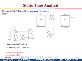
21.
Static Time Analysis
CommonPath & Clock Reconvergence Pessimism
Removal
Launch path is c3->c4->m1
The capture path c1->m1->c5
Clock reconvergence
pessimism: 1.4ns
Source: https://vlsi.pro/common-path-clock-reconvergence-pessimism-
removal/
8/19/2023
ELECTRICAL
21
ELECTRONICS COMMUNICATION INSTRUMENTATION
22.
Static Time Analysis
8/19/2023
ELECTRICAL
22
INSTRUMENTATIO
ELECTRONICSCOMMUNICATION
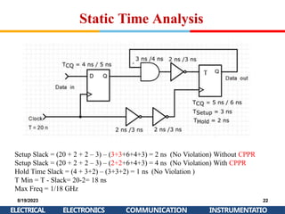
Setup Slack = (20 + 2 + 2 – 3) – (3+3+6+4+3) = 2 ns (No Violation) Without CPPR
Setup Slack = (20 + 2 + 2 – 3) – (2+2+6+4+3) = 4 ns (No Violation) With CPPR
Hold Time Slack = (4 + 3+2) – (3+3+2) = 1 ns (No Violation )
T Min = T - Slack= 20-2= 18 ns
Max Freq = 1/18 GHz
23.
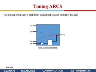
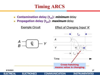
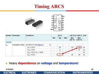
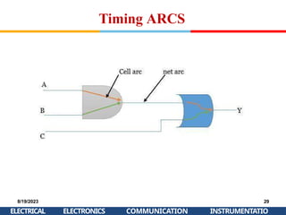
Timing ARCS
The timingarc means a path from each input to each output of the cell.
8/19/2023
ELECTRICAL
23
INSTRUMENTATIO
ELECTRONICS COMMUNICATION
24.
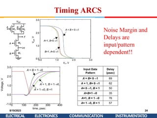
Timing ARCS
Noise Marginand
Delays are
input/pattern
dependent!!
8/19/2023
ELECTRICAL
24
INSTRUMENTATIO
ELECTRONICS COMMUNICATION
25.
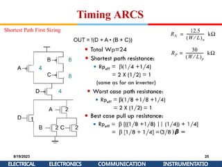
Timing ARCS
( )𝞫=
0.75
Shortest Path First Sizing
8/19/2023
ELECTRICAL
25
INSTRUMENTATIO
ELECTRONICS COMMUNICATION
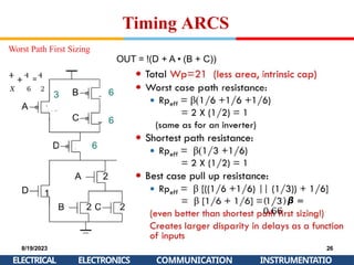
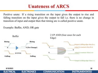
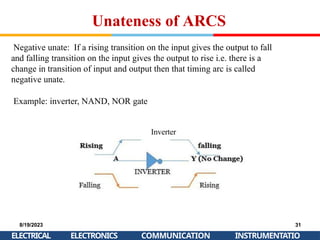
Unateness of ARCS
Positiveunate: If a rising transition on the input gives the output to rise and
falling transition on the input gives the output to fall i.e. there is no change in
transition of input and output then that timing arc is called positive unate.
Example: Buffer, AND, OR gate
Buffer
2 I/P AND (four cases for each
Edge)
8/19/2023
ELECTRICAL
30
INSTRUMENTATIO
ELECTRONICS COMMUNICATION
31.
Unateness of ARCS
Negativeunate: If a rising transition on the input gives the output to fall
and falling transition on the input gives the output to rise i.e. there is a
change in transition of input and output then that timing arc is called
negative unate.
Example: inverter, NAND, NOR gate
Inverter
8/19/2023
ELECTRICAL
31
INSTRUMENTATIO
ELECTRONICS COMMUNICATION
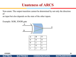
32.
Unateness of ARCS
Non-unate:The output transition cannot be determined by not only the direction
of
an input but also depends on the state of the other inputs.
Example: XOR, XNOR gate
8/19/2023
ELECTRICAL
32
INSTRUMENTATIO
ELECTRONICS COMMUNICATION
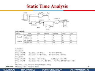
Path Based Delay
8/19/2023
ELECTRICAL
36
INSTRUMENTATIO
ELECTRONICSCOMMUNICATION
Path A-Y Max Delay = 2+12+2+13+3+6 = 38 ps Min Delay = 1+10+1+11+2+5=
30
Path B-Y Max Delay = 2+14+2+13+3+6 = 40 ps Min Delay = 1+12+1+11+2+5=
32
Path C-Y Max Delay = 4+15+3+6 = 28 ps Min Delay = 2+13+2+5= 22
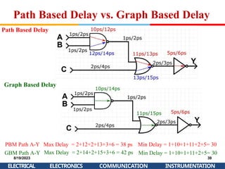
37.
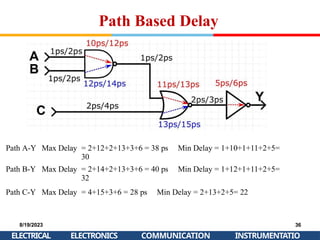
Path Based Delayvs. Graph Based Delay
PBM Path A-Y Max Delay = 2+12+2+13+3+6 = 38
ps GBM Path A-Y Max Delay =
2+14+2+15+3+6 = 42 ps
Min Delay = 1+10+1+11+2+5= 30
Min Delay = 1+10+1+11+2+5= 30
Path Based Delay
Graph Based Delay
8/19/2023
ELECTRICAL
37
INSTRUMENTATIO
ELECTRONICS COMMUNICATION
38.
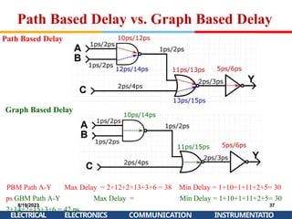
Path Based Delayvs. Graph Based Delay
Path B-Y Max Delay = 2+14+2+13+3+6 = 40 ps Min Delay = 1+12+1+11+2+5= 32
Path Based Delay
Graph Based Delay
GBM Path B-Y
8/19/2023
ELECTRICAL
Max Delay = 2+14+2+15+3+6 = 42 ps Min Delay = 1+10+1+11+2+5= 30
38
ELECTRONICS COMMUNICATION INSTRUMENTATION
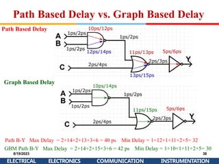
39.
PBM Path A-YMax Delay = 2+12+2+13+3+6 = 38 ps Min Delay = 1+10+1+11+2+5= 30
GBM Path A-Y
8/19/2023
Max Delay = 2+14+2+15+3+6 = 42 ps Min Delay = 1+10+1+11+2+5= 30
39
Path Based Delay vs. Graph Based Delay
Path Based Delay
Graph Based Delay
ELECTRICAL ELECTRONICS COMMUNICATION INSTRUMENTATION
40.
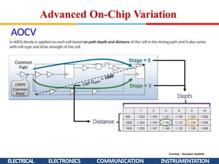
AOCV
In A0CV derateis applied on each cell based on path depth and distance of the cell in the timing path and it also varies
with cell type and drive strength of the cell.
Courtesy : Synopsys AppNote
ELECTRICAL ELECTRONICS COMMUNICATION INSTRUMENTATION
Advanced On-Chip Variation
41.
Limitations of AOCV
ELECTRICALELECTRONICS COMMUNICATION INSTRUMENTATION
• The AOCV's distance and depth-based derate factor works well for
technology nodes over 40 nm, but we still need to make it better for
nodes below that.
• POCV models timing as true statistical distributions
–Delay/Transition/Constraint variation modeling
• In technology nodes 20nm and below, POCV is particularly efficient.
Advanced On-Chip Variation
42.
POCV
ELECTRICAL ELECTRONICS COMMUNICATIONINSTRUMENTATION
• In POCV instead of applying the specific derate factor to a cell, cell delay is calculated based
on delay variation (σ) of the cell.
• In other words, the instance delay is parameterized as a function of this
random variable.
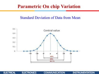
Parametric On chip Variation
43.
Standard Deviation ofData from Mean
Parametric On chip Variation
ELECTRICAL ELECTRONICS COMMUNICATION INSTRUMENTATION

![Static Time Analysis
𝑆𝑒𝑡𝑢𝑝 𝑆𝑙𝑎𝑐𝑘 = [100 𝑇
+
10
− 10 𝐶1
𝐶1 + 30 𝐵1 − 𝐵3 −
30(𝑡𝑠𝑒𝑡𝑢𝑝)]
+ 10 𝐴1+ 50 FF1 + 20
G1 = 20 ps
𝐻𝑜𝑙𝑑 𝑆𝑙𝑎𝑐𝑘 = [10 𝐶1 + 10 𝐴1 + 50
𝐹𝐹1 + 20(𝐺1)]
− 10 𝐶1 + 30 𝐵1 − 𝐵3
+ 20(𝑡ℎ𝑜𝑙𝑑) =
30 ps
8/19/2023
ELECTRICAL
18
INSTRUMENTATIO
ELECTRONICS COMMUNICATION
𝑇 =
100 𝑝𝑠](https://image.slidesharecdn.com/lec-05sta-1-250217151236-1a8d85a0/85/Lec-05_Static-timing-analysis-digital-vlsi-design-18-320.jpg)
![Static Time Analysis
𝑆𝑒𝑡𝑢𝑝 𝑆𝑙𝑎𝑐𝑘 =
{100 𝑇
+
10 𝐶1 + 30 𝐵1 − 𝐵3 ∗ 0.9 −30 𝑡𝑠𝑒𝑡𝑢𝑝 }
− 10 𝐶1+ 10 𝐴1 + 50 FF1 +
20 G1 ∗ 1.1 = ⋯ … . .
On chip
− variation (OCV) 𝑒𝑔. 10% 𝐿𝑎𝑡𝑒 −
10% 𝐸𝑎𝑟𝑙𝑦
𝐻𝑜𝑙𝑑 𝑆𝑙𝑎𝑐𝑘 = {[10 𝐶1 + 10 𝐴1 + 50 𝐹𝐹1
+ 20(𝐺1)] ∗ 0.9}
−{ 10 𝐶1 + 30 𝐵1 − 𝐵3 ] ∗ 1.1 +
20(𝑡ℎ𝑜𝑙𝑑) } = ⋯ . . ps
8/19/2023
ELECTRICAL
19
INSTRUMENTATIO
ELECTRONICS COMMUNICATION](https://image.slidesharecdn.com/lec-05sta-1-250217151236-1a8d85a0/85/Lec-05_Static-timing-analysis-digital-vlsi-design-19-320.jpg)


![[Back2School] Timing Verification- Chapter 4](https://cdn.slidesharecdn.com/ss_thumbnails/timingverification-250607212312-4e8e2612-thumbnail.jpg?width=640&height=640&fit=bounds)


![[Back2School] Constraint Develop.pdf- Chapter 3](https://cdn.slidesharecdn.com/ss_thumbnails/constraintdevelop-250606153235-d8296a49-thumbnail.jpg?width=640&height=640&fit=bounds)


