Finite State Machines
•Finite State Machines (FSM) are sequential circuit
used in many digital systems to control the
behavior of systems and dataflow paths. Examples
of FSM include control units and sequencers
• The state machines are modeled using two basic
types of sequential networks- Mealy and Moore.
In a Mealy machine, the output depends on both
the present (current) state and the present
(current) inputs. In Moore machine, the output
depends only on the present state.
3.
Mealy FSM
• Ageneral model of a Mealy sequential machine consists of a combinatorial
network, which generates the outputs and the next state, and a state register
which holds the present state as shown below. The state register is normally
modeled as D flip-flops. The state register must be sensitive to a clock edge. The
other block(s) can be modeled either using the always procedural block or a
mixture of the always procedural block and dataflow modeling statements; the
always procedural block will have to be sensitive to all inputs being read into the
block and must have all output defined for every branch in order to model it as a
combinatorial block.
• The two blocks Mealy machine fig 1 The Three block Moore machine fig2
Fig1. Fig2.
Moore FSM
• Ageneral model of a Moore sequential machine is shown below. Its output is
generated from the state register block. The next state is determined using the
present (current) input and the present (current) state. Here the state register is
also modeled using D flip-flops. Normally Moore machines are described using
three blocks, one of which must be a sequential and the other two can be
modeled using always blocks or a combination of always and dataflow modeling
constructs.
Meta-stability
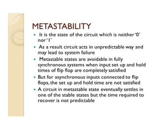
• In Generalmeta-stability is an un-avoidable behavior of the circuit that may cause
malfunction.
• From a specification point of view, synchronous elements such as flip flops specify a setup
time and hold time. (setup time: data should be stable for this time before arrival of clock)
(Hold time: data should be hold stable for this time after arrival of clock).
• Clock calculation depends upon setup time hold time and propagation delay
• If setup and hold time is violated then meta-stability will occur.
13.
WHAT IS METASTABILITY?
•Meta-stability in digital systems occurs when two
asynchronous signals combine in such a way that their
resulting output goes to an indeterminate state.
• A common example is the case of data violating the setup and
hold specifications of a latch or a flip-flop.
• In an ideal world, where all logic designs are synchronous and
all inputs are tied to the system clock, meta-stability would
not be a concern because all timing conditions for the flip-
flops would be met.
• However, in most of the design, the data is asynchronous
w.r.t. the clock making the flop a potential candidate for meta-
stability as there’s no reasonable way to insure that the
changing asynchronous data will meet the flop’s setup time.
Occasionally – not often - the latched data will be corrupt. So
the designer has to take care of these violations.
14.
WHAT ARE THECASES, WHEN METASTABILITY
OCCURS?
• As we have seen that whenever setup and hold violation
time occurs, meta-stability occurs, so it is to be seen when
does this signal violate this timing requirement.
• When the input signal is a asynchronous signal
• When the clock skew is more (rise time and fall time is
more then the tolerable values).
• When interfacing two domains operating at two different
frequency.
• When the combinational delay is such way that, it changes
flip-flop’s input in the required window (setup + hold
window)
15.
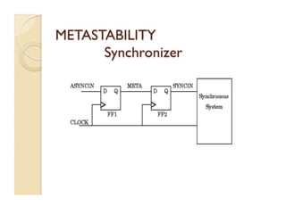
HOW TO MINIMIZEMETASTABILITY?
• Synchronize any asynchronous input through one path that has at least
one and preferably two flip-flops in series. The flip-flops should be running
on the same edge of your system clock as the rest of the circuit.
• Design any state machines whose operation is affected by these
“synchronized” signals to follow a gray code pattern between states
controlled by these signals. Gray Code is a counting scheme where only a
single bit changes between numbers
• Ensure that setup time of the destination flip-flop is met. This will avoid
the creation of metastable conditions inside the circuit and minimize the
propagation of any should they occur.
• Compute a parity or checksum of the input data before the capture
register. Latch that into the register as well. Have the code compute parity
and compare it to that read. If there's an error, do another read.
• Use metastability hardened Flip-flops.
16.
Noise margin
• Noisemargin is a parameter closely related to the input-output voltage
characteristics. This parameter allows us to determine the allowable noise
voltage on the input of gate so that the output will not be affected.
• The specification most commonly used to specify noise margin in terms of
two parameters. LOW noise Margin NML and High noise Margin NMH
17.
Noise Margin
• Notethat if either NML or NMH for gate are reduced below
0.1*Vdd, then the gate may be susceptible to switching noise
that may be present on the inputs. Apart from considering a
single gate , one must consider the net effect of noise sources
and noise margins on cascaded gates in assessing the overall
noise immunity of a particular system.
• Quite often noise margins are compromised to improve speed
of the circuit.
Speed Performance
• Worstcase rise delay= (Rp/n)*(m*n*Cd+Cr+kCg)
gate ,drain, routing capacitance, effective resistance of p device in
this gate, m-fan-in of gate,k-fanout,n width multiplier of p-device.
• Fall delay time = (Rn/n)*(m*n*r*Cg+q(k)*Cg+k*Cg))
• Rp=mRn
• BpWp=BnWn/m
• *q(k) function of routing capacitance
21.
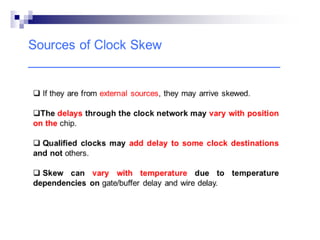
Clock skew
• Clockskew is a phenomenon in synchronous circuits in
which the clock signal (sent from the clock circuit or
source or clock definition point) arrives at different
components at different times.
due to
• wire-interconnect length
• temperature variations
• capacitive coupling
• material imperfections and
• differences in input capacitance on the clock inputs
• these factor became more critical for high frequency
22.
Clock Skew--
• Negativeskew
• positive skew
• Positive skew occurs when the transmitting register receives
the clock tick earlier than the receiving register.
Negative skew is occurs when the receiving register gets the
clock tick earlier than the sending reg
• Zero clock skew refers to the arrival of the clock tick
simultaneously at transmitting and receiving reg
• Useful Skew
clock skew can also benefit a circuit by decreasing the clock
period locally at which the circuit will operate correctly, it
means skew add more margin to meet setup. that is called
useful skew
25.
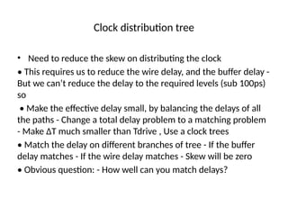
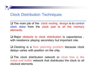
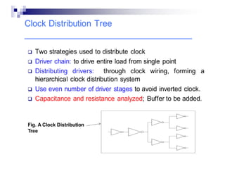
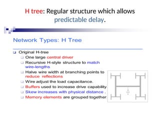
Clock distribution tree
•Need to reduce the skew on distributing the clock
• This requires us to reduce the wire delay, and the buffer delay -
But we can’t reduce the delay to the required levels (sub 100ps)
so
• Make the effective delay small, by balancing the delays of all
the paths - Change a total delay problem to a matching problem
- Make ∆T much smaller than Tdrive , Use a clock trees
• Match the delay on different branches of tree - If the buffer
delay matches - If the wire delay matches - Skew will be zero
• Obvious question: - How well can you match delays?
Clock Jitter
• Jitteris the timing variations of a set of signal
edges from their ideal values. Jitters in clock
signals are typically caused by noise or other
disturbances in the system.
• Contributing factors include thermal noise,
power supply variations, loading conditions,
device noise, and interference coupled from
nearby circuits.
35.
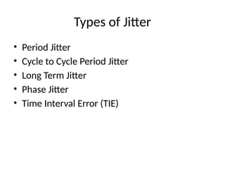
Types of Jitter
•Period Jitter
• Cycle to Cycle Period Jitter
• Long Term Jitter
• Phase Jitter
• Time Interval Error (TIE)
36.
Period jitter
• Periodjitter is the deviation in cycle time of a clock
signal with respect to the ideal period over a number
of randomly selected cycles.
• If we were given a number of individual clock
periods, we can measure each one and calculate the
average clock period as well as the standard
deviation and the peak-to-peak value.
• The standard deviation and the peak-to-peak value
are frequently referred to as the RMS value and the
Pk-Pk period jitter, respectively.
37.
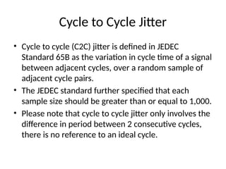
Cycle to CycleJitter
• Cycle to cycle (C2C) jitter is defined in JEDEC
Standard 65B as the variation in cycle time of a signal
between adjacent cycles, over a random sample of
adjacent cycle pairs.
• The JEDEC standard further specified that each
sample size should be greater than or equal to 1,000.
• Please note that cycle to cycle jitter only involves the
difference in period between 2 consecutive cycles,
there is no reference to an ideal cycle.
38.
Long term jitter
•Long-term jitter measures the change in a clock’s output
from the ideal position, over several consecutive cycles.
• The actual number of cycles used in the measurement is
application dependent.
• Long-term jitter is different from period jitter and cycle-
to-cycle jitter because it represents the cumulative
effect of jitter on a continuous stream of clock cycles
over a long time interval. That is why long-term jitter is
sometimes referred to as the accumulated jitter.
• Long term jitter is typically useful in graphics/video
displays and long-range telemetry applications such as
range finders.
39.
Phase jitter
• Phasenoise is usually described as either a set
of noise values at different frequency offsets
(e.g., -60 dBc/Hz –(decibels relative to the
carrier per Hertz) at 20KHz and -95 dBc/Hz at
10MHz), or as a continuous noise plot over a
range of frequencies.
• Phase jitter is the integration of phase noises
over a certain spectrum and expressed in
seconds.
43.
Supply and groundbounce
• As a module is clocked , the current drawn from the power-
supply leads tends to rise as the clock transition.
• The current reflects various stages of logic triggered by values
changing due to clock transition.
• Any gate may change close to clock, large spike may occur.
• This is lead to what is termed as “ground bounce” for ground
lead and Supply bounce for supply lead.
• Ground bounce can also occur in I/O Pads.
• Clock buffer can also cause considerable ground bounce in
supply leads.
47.
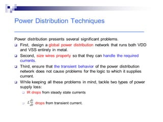
Power distribution Techniques
•Power distribution presents several significant problems.
• First we must design a global power distribution network that
runs both VDD and Vss entirely in metal.
• We must size wire properly so that they can handle require
current.
• We must ensure that the transient behavior of the
distribution N/W does not cause a problem for logic to which
it supplies current.
• Tackle power supply loss (IR loss)
• Tackle power supply loss (I*di/dt loss).
52.
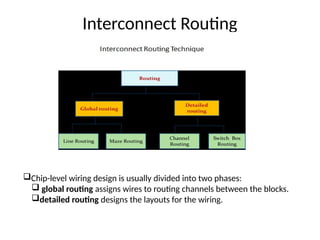
Interconnect Routing
Chip-level wiringdesign is usually divided into two phases:
global routing assigns wires to routing channels between the blocks.
detailed routing designs the layouts for the wiring.
53.
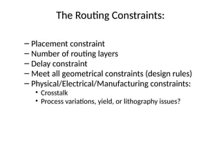
The Routing Constraints:
–Placement constraint
– Number of routing layers
– Delay constraint
– Meet all geometrical constraints (design rules)
– Physical/Electrical/Manufacturing constraints:
• Crosstalk
• Process variations, yield, or lithography issues?
56.
Line Probe
Routing:
• LetS and T denote a pair of
terminals to be connected.
• Basic idea:
Assume no obstacles for the time being.
A vertical line drawn through S and a
horizontal line passing though T will intersect .
• In the presence of obstacles,
several such lines need to be
drawn.
• Line search algorithms do not
guarantee finding the optimal
path. – May need several
backtrackings. – Running time
and memory requirements are
significantly less. – Routing area
and paths are represented by a
set of line segments.
57.
Maze Routing
• Given:
–A planar rectangular grid graph.
– Two points S and T on the graph.
– Obstacles modeled as blocked
vertices.
• Objective:
– Find the shortest path connecting
S and T.
• This technique can be used in global
or detailed routing (switchbox)
problems.
58.
Detailed Routing
• Threetypes of detailed routing methods:
Channel Routing
2-D Switchbox Routing
3-D Switchbox Routing
• Channel routing → 2-D switchbox → 3-D
switchbox
• If the switchbox or channels are unroutable
without a large expansion, global routing
needs to be done again.
59.
• Channel routing:
channel may grow in one dimension to accommodate
wires;
pins generally on only two opposite sides.
• Channel routing is a special case of the routing
problem in which wires are connected within the
routing channels.
• To apply channel routing, a routing region is usually
decomposed into routing channels.
60.
• Switchbox routing:
Switch box routing is
harder than channel
routing because we
can’t expand the
switchbox to make
room for more wires.
pins are on all four
sides, fixing
dimensions of the box.
61.
Power Optimization: LogicGates
___________________________________
Reduce Power consumption of isolated gate logic
To make it change its output as few times as possible.
Number of unnecessary changes to a gate’s output.
The gate would not be useful if it never changed its output
value.
To reduce the number of unnecessary changes to a gate’s
output
62.
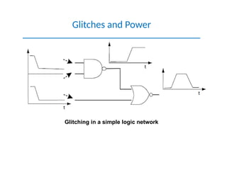
Glitching in asimple logic network
Glitches and Power
_______________________________________________
63.
• Some sourcesof glitches are more systematic and easier to
eliminate.
Sources of Glitches
___________________________________
Glitching in a chain of adders.
64.
• Need tobe able to estimate the signal probabilities in the
network.
• The signal probability Ps is the probability that signal s is 1.
• The probability of a transition Ptr,s can be derived from the
signal probability, assuming that the signal’s values on clock
cycles are independent:
Ptr,s = 2Ps(1-Ps)
Signal Probabilities
___________________________________
65.
Delay-independent and delay-dependentpower estimation
___________________________________
There are two major ways to compute signal probabilities and power
consumption:
1. delay-independent and
2. delay-dependent.
Analysis based on delay-independent signal probabilities is less accurate
than delay-dependent analysis but delay-independent values can be
computed much more quickly.
66.
The time/accuracy trade-offsfor power estimation
track those for delay estimation:
1. circuit level methods are the most accurate and
costly;
2. switch-level simulation is somewhat less accurate
but more efficient;
3. logic-based simulation is less powerful but can
handle larger networks.
67.
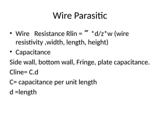
Wire Parasitic
• WireResistance Rlin = *d/z*w (wire
resistivity ,width, length, height)
• Capacitance
Side wall, bottom wall, Fringe, plate capacitance.
Cline= C.d
C= capacitance per unit length
d =length
74.
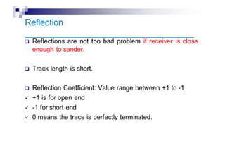
Signal Integrity Issues
•Reflection noise: Due to impedance mismatch,
stubs, vias and other discontinuity
• Cross talk: Due to electromagetic coupling
between signal and vias
• Power ground noise: Ground bounce and
power bounce
• Packaging: Packaging interconnect structure
88.
• The placementof pads around the ring is usually determined
by the required order of pins on the package.
• The wires to the package cannot be crossed without danger of
shorting, so if the package pins are required in a certain order,
the pads must be arranged in that order.
• The order of pins on the package determines routability of the
board and electrical noise among other things.
• The order of pins on a package has been known to determine
which candidate design wins a design contest.


![[Back2School] Constraint Develop.pdf- Chapter 3](https://cdn.slidesharecdn.com/ss_thumbnails/constraintdevelop-250606153235-d8296a49-thumbnail.jpg?width=640&height=640&fit=bounds)


