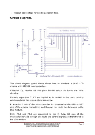
TAPI DIPLOMA ENGINEERING COLLEGE, SURAT Page 1
ELECTRICAL ENGINEERING DEPARTMENT
EXPERIMENT NO: ________ DATE: _______
AIM: Interface LCD display with 8051 kit.
OBJECTIVES:
• To understand Interface of LCD display with 8051 kit.
THEORY
16×2 LCD module.
16×2 LCD module is a very common type of LCD module. It consists of 16
rows and 2 columns of 5×7 or 5×8 LCD dot matrices. It is available in a 16
pin package with back light, contrast adjustment function and each dot
matrix has 5×8 dot resolution. The pin numbers, their name and
corresponding functions are shown in the table below.
Pin No: Name Function
1 VSS This pin must be connected to the ground
2 VCC Positive supply voltage pin (5V DC)
3 VEE Contrast adjustment
4 RS Register selection
5 R/W Read or write
6 E Enable
7 DB0 Data
8 DB1 Data
9 DB2 Data
10 DB3 Data
11 DB4 Data
12 DB5 Data
13 DB6 Data
14 DB7 Data
15 LED+ Back light LED+
16 LED- Back light LED-
VEE pin is meant for adjusting the contrast of the LCD display and the
contrast can be adjusted by varying the voltage at this pin. This is done by
connecting one end of a POT to the Vcc (5V), other end to the Ground and
connecting the center terminal (wiper) of of the POT to the VEE pin.
It has two built in registers namely data register and command
register. Data register is for placing the data to be displayed and the
command register is to place the commands.
TAPI DIPLOMA ENGINEERING COLLEGE, SURAT Page 2
ELECTRICAL ENGINEERING DEPARTMENT
The 16×2 LCD module has a set of commands each meant for doing a
particular job with the display.
High logic at the RS pin will select the data register and Low logic at the RS
pin will select the command register. If RS pin is high and the put a data
in the 8 bit data line (DB0 to DB7), the LCD module will recognize it as a
data to be displayed. If RS pin is low and put a data on the data line, the
module will recognize it as a command.
R/W pin is meant for selecting between read and write modes. High level at
this pin enables read mode and low level at this pin enables write mode.
E pin is for enabling the module. A high to low transition at this pin will
enable the module.
DB0 to DB7 are the data pins. The data to be displayed and the command
instructions are placed on these pins.
LED+ is the anode of the back light LED and this pin must be connected to
VCC through a suitable series current limiting resistor. LED- is the cathode
of the back light LED and this pin must be connected to ground.
16×2 LCD module commands.
16×2 LCD module has a set of preset command instructions. Each
command will make the module to do a particular task. The commonly
used commands and their function are given in the table below.
Command Function
0F LCD ON, Cursor ON, Cursor blinking ON
01 Clear screen
02 Return home
04 Decrement cursor
06 Increment cursor
0E Display ON ,Cursor blinking OFF
80 Force cursor to the beginning of 1st line
TAPI DIPLOMA ENGINEERING COLLEGE, SURAT Page 3
ELECTRICAL ENGINEERING DEPARTMENT
Command Function
C0 Force cursor to the beginning of 2nd line
38 Use 2 lines and 5×7 matrix
83 Cursor line 1 position 3
3C Activate second line
08 Display OFF, Cursor OFF
C1 Jump to second line, position1
OC Display ON, Cursor OFF
C1 Jump to second line, position1
C2 Jump to second line, position2
LCD initialization.
The steps that has to be done for initializing the LCD display is given below
and these steps are common for almost all applications.
 Send 38H to the 8 bit data line for initialization.
 Send 0FH for making LCD ON, cursor ON and cursor blinking ON.
 Send 06H for incrementing cursor position.
 Send 01H for clearing the display and return the cursor.
Sending data to the LCD.
The steps for sending data to the LCD module is given below. It is the logic
state of these pins that make the module to determine whether a given
data input is a command or data to be displayed.
 Make R/W low.
 Make RS=0 if data byte is a command and make RS=1 if the data byte
is a data to be displayed.
 Place data byte on the data register.
 Pulse E from high to low.
TAPI DIPLOMA ENGINEERING COLLEGE, SURAT Page 4
ELECTRICAL ENGINEERING DEPARTMENT
 Repeat above steps for sending another data.
Circuit diagram.
The circuit diagram given above shows how to interface a 16×2 LCD
module with AT89S1 microcontroller.
Capacitor C3, resistor R3 and push button switch S1 forms the reset
circuitry.
Ceramic capacitors C1,C2 and crystal X1 is related to the clock circuitry
which produces the system clock frequency.
P1.0 to P1.7 pins of the microcontroller is connected to the DB0 to DB7
pins of the module respectively and through this route the data goes to the
LCD module.
P3.3, P3.4 and P3.5 are connected to the E, R/W, RS pins of the
microcontroller and through this route the control signals are transffered to
the LCD module.
TAPI DIPLOMA ENGINEERING COLLEGE, SURAT Page 5
ELECTRICAL ENGINEERING DEPARTMENT
Resistor R1 limits the current through the back light LED and so do the back
light intensity. POT R2 is used for adjusting the contrast of the display.
Conclusion:
_____________________________________________________
_____________________________________________________
__________________________________________________
Short Questions:
1. How much total external data memory that can be interfaced to the
8051?
2. Write format of PSW for 8051.

LCD WITH 8051.docx

  • 1.
    TAPI DIPLOMA ENGINEERINGCOLLEGE, SURAT Page 1 ELECTRICAL ENGINEERING DEPARTMENT EXPERIMENT NO: ________ DATE: _______ AIM: Interface LCD display with 8051 kit. OBJECTIVES: • To understand Interface of LCD display with 8051 kit. THEORY 16×2 LCD module. 16×2 LCD module is a very common type of LCD module. It consists of 16 rows and 2 columns of 5×7 or 5×8 LCD dot matrices. It is available in a 16 pin package with back light, contrast adjustment function and each dot matrix has 5×8 dot resolution. The pin numbers, their name and corresponding functions are shown in the table below. Pin No: Name Function 1 VSS This pin must be connected to the ground 2 VCC Positive supply voltage pin (5V DC) 3 VEE Contrast adjustment 4 RS Register selection 5 R/W Read or write 6 E Enable 7 DB0 Data 8 DB1 Data 9 DB2 Data 10 DB3 Data 11 DB4 Data 12 DB5 Data 13 DB6 Data 14 DB7 Data 15 LED+ Back light LED+ 16 LED- Back light LED- VEE pin is meant for adjusting the contrast of the LCD display and the contrast can be adjusted by varying the voltage at this pin. This is done by connecting one end of a POT to the Vcc (5V), other end to the Ground and connecting the center terminal (wiper) of of the POT to the VEE pin. It has two built in registers namely data register and command register. Data register is for placing the data to be displayed and the command register is to place the commands.
  • 2.
    TAPI DIPLOMA ENGINEERINGCOLLEGE, SURAT Page 2 ELECTRICAL ENGINEERING DEPARTMENT The 16×2 LCD module has a set of commands each meant for doing a particular job with the display. High logic at the RS pin will select the data register and Low logic at the RS pin will select the command register. If RS pin is high and the put a data in the 8 bit data line (DB0 to DB7), the LCD module will recognize it as a data to be displayed. If RS pin is low and put a data on the data line, the module will recognize it as a command. R/W pin is meant for selecting between read and write modes. High level at this pin enables read mode and low level at this pin enables write mode. E pin is for enabling the module. A high to low transition at this pin will enable the module. DB0 to DB7 are the data pins. The data to be displayed and the command instructions are placed on these pins. LED+ is the anode of the back light LED and this pin must be connected to VCC through a suitable series current limiting resistor. LED- is the cathode of the back light LED and this pin must be connected to ground. 16×2 LCD module commands. 16×2 LCD module has a set of preset command instructions. Each command will make the module to do a particular task. The commonly used commands and their function are given in the table below. Command Function 0F LCD ON, Cursor ON, Cursor blinking ON 01 Clear screen 02 Return home 04 Decrement cursor 06 Increment cursor 0E Display ON ,Cursor blinking OFF 80 Force cursor to the beginning of 1st line
  • 3.
    TAPI DIPLOMA ENGINEERINGCOLLEGE, SURAT Page 3 ELECTRICAL ENGINEERING DEPARTMENT Command Function C0 Force cursor to the beginning of 2nd line 38 Use 2 lines and 5×7 matrix 83 Cursor line 1 position 3 3C Activate second line 08 Display OFF, Cursor OFF C1 Jump to second line, position1 OC Display ON, Cursor OFF C1 Jump to second line, position1 C2 Jump to second line, position2 LCD initialization. The steps that has to be done for initializing the LCD display is given below and these steps are common for almost all applications.  Send 38H to the 8 bit data line for initialization.  Send 0FH for making LCD ON, cursor ON and cursor blinking ON.  Send 06H for incrementing cursor position.  Send 01H for clearing the display and return the cursor. Sending data to the LCD. The steps for sending data to the LCD module is given below. It is the logic state of these pins that make the module to determine whether a given data input is a command or data to be displayed.  Make R/W low.  Make RS=0 if data byte is a command and make RS=1 if the data byte is a data to be displayed.  Place data byte on the data register.  Pulse E from high to low.
  • 4.
    TAPI DIPLOMA ENGINEERINGCOLLEGE, SURAT Page 4 ELECTRICAL ENGINEERING DEPARTMENT  Repeat above steps for sending another data. Circuit diagram. The circuit diagram given above shows how to interface a 16×2 LCD module with AT89S1 microcontroller. Capacitor C3, resistor R3 and push button switch S1 forms the reset circuitry. Ceramic capacitors C1,C2 and crystal X1 is related to the clock circuitry which produces the system clock frequency. P1.0 to P1.7 pins of the microcontroller is connected to the DB0 to DB7 pins of the module respectively and through this route the data goes to the LCD module. P3.3, P3.4 and P3.5 are connected to the E, R/W, RS pins of the microcontroller and through this route the control signals are transffered to the LCD module.
  • 5.
    TAPI DIPLOMA ENGINEERINGCOLLEGE, SURAT Page 5 ELECTRICAL ENGINEERING DEPARTMENT Resistor R1 limits the current through the back light LED and so do the back light intensity. POT R2 is used for adjusting the contrast of the display. Conclusion: _____________________________________________________ _____________________________________________________ __________________________________________________ Short Questions: 1. How much total external data memory that can be interfaced to the 8051? 2. Write format of PSW for 8051.