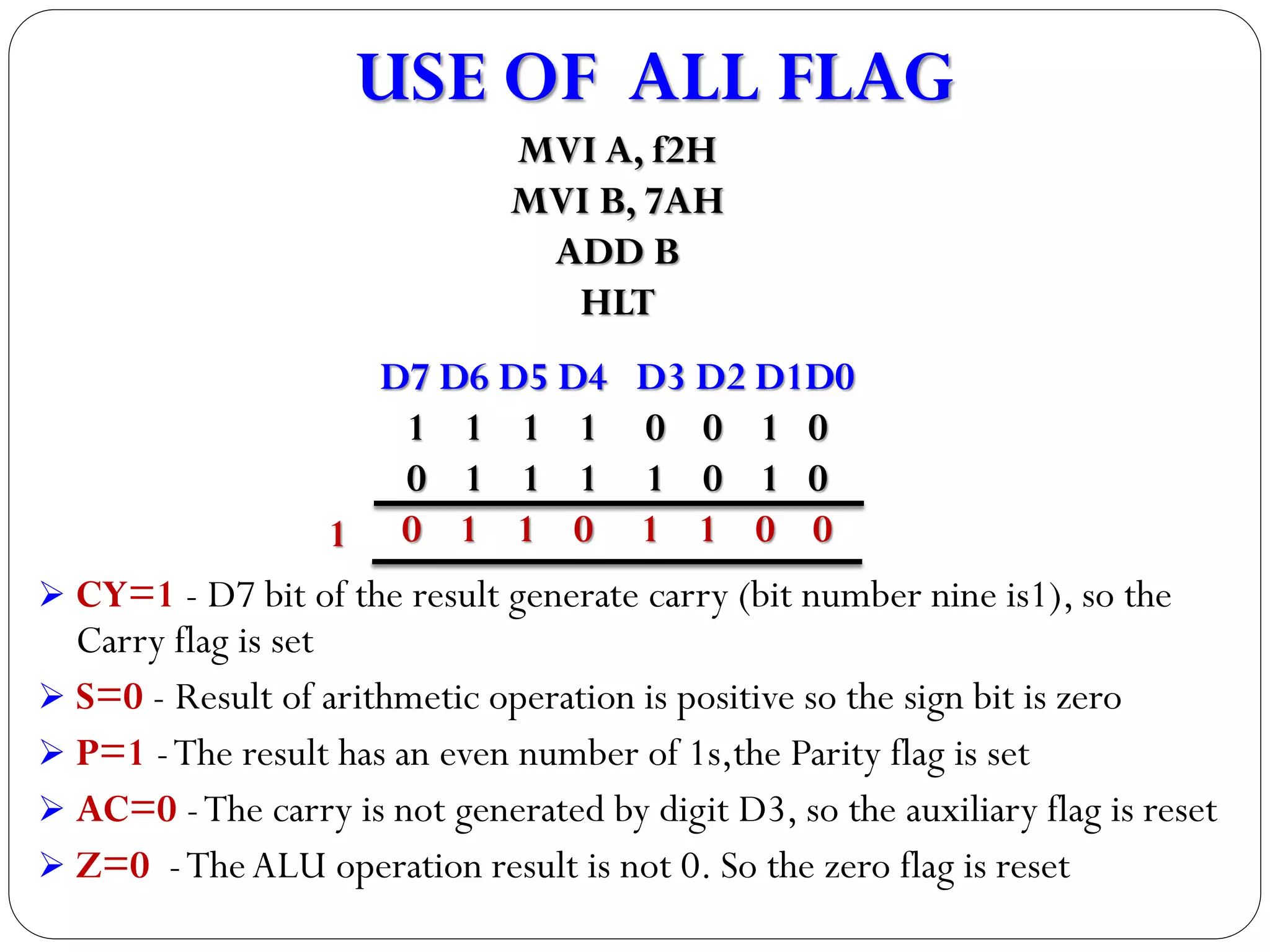
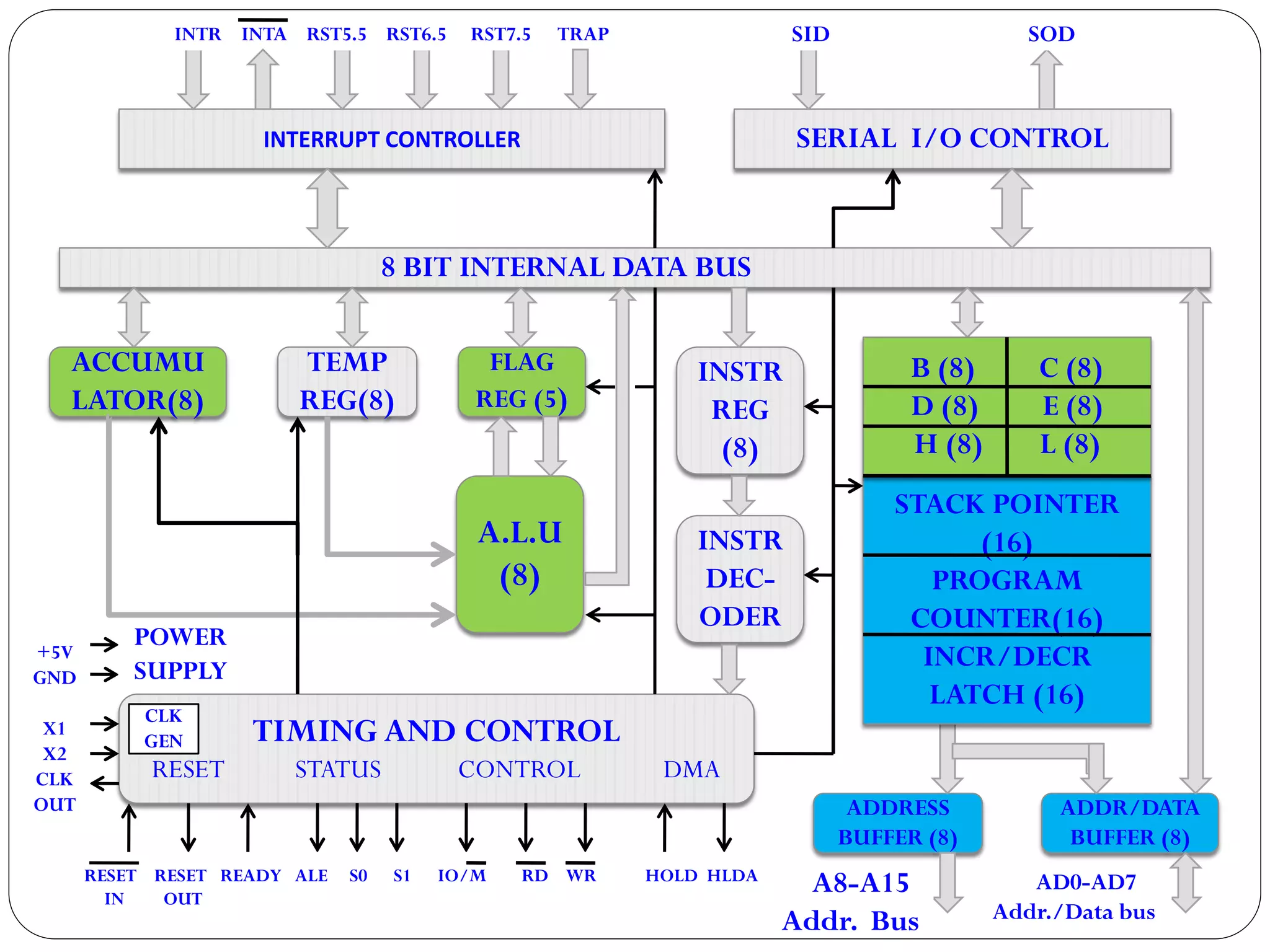
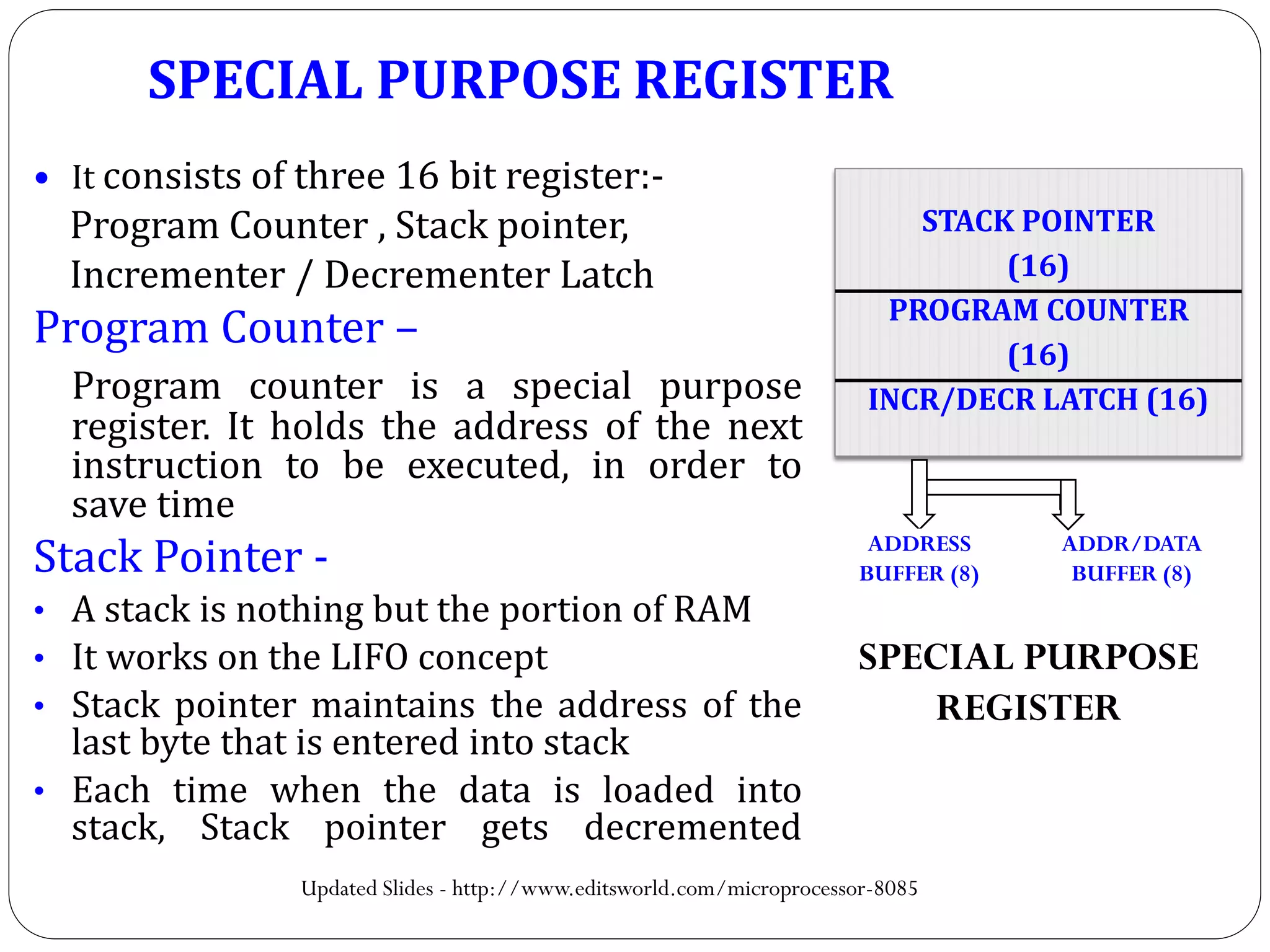
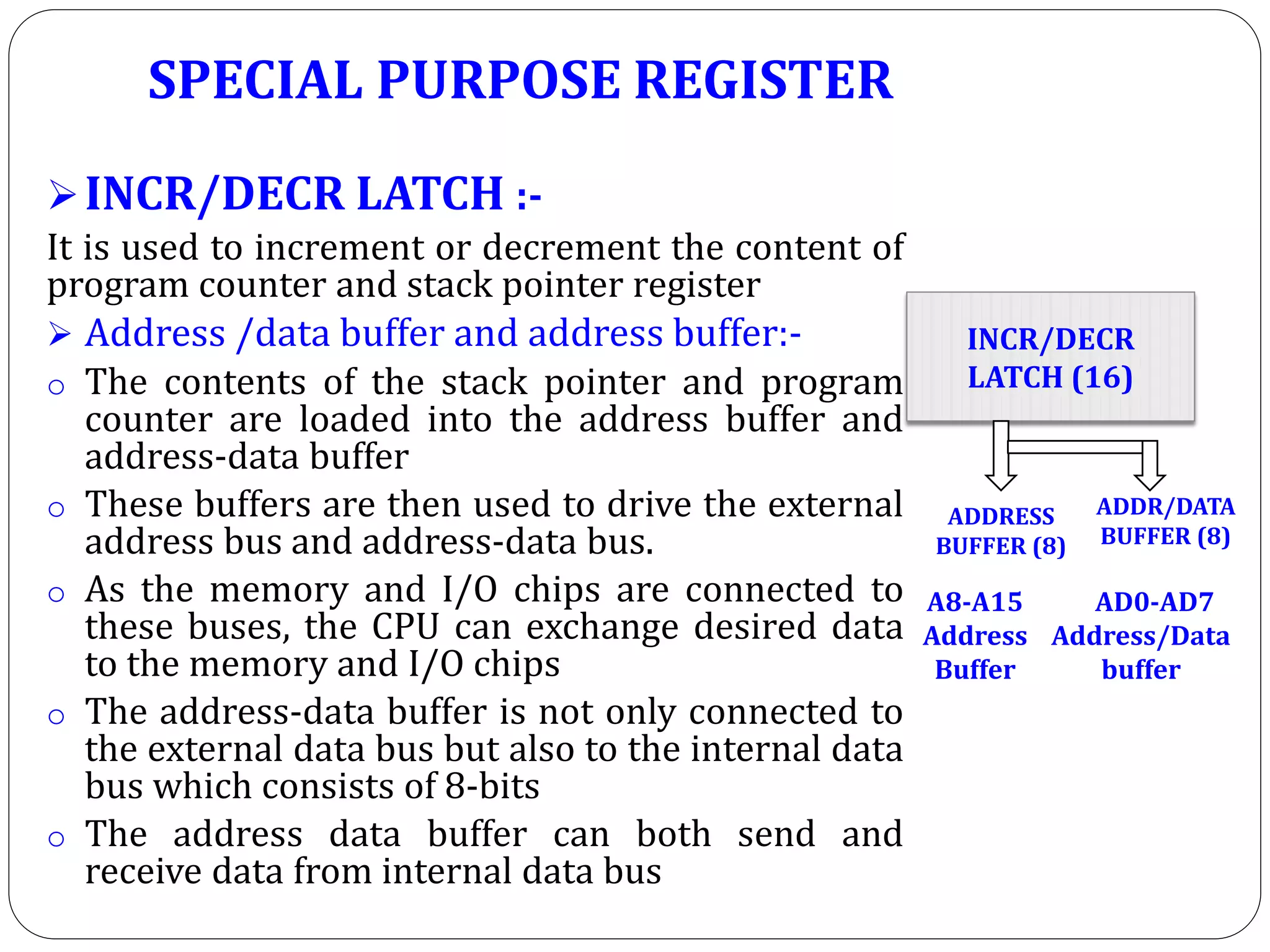
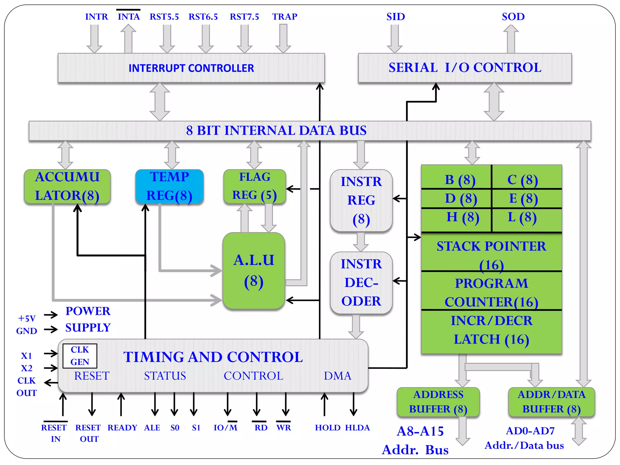
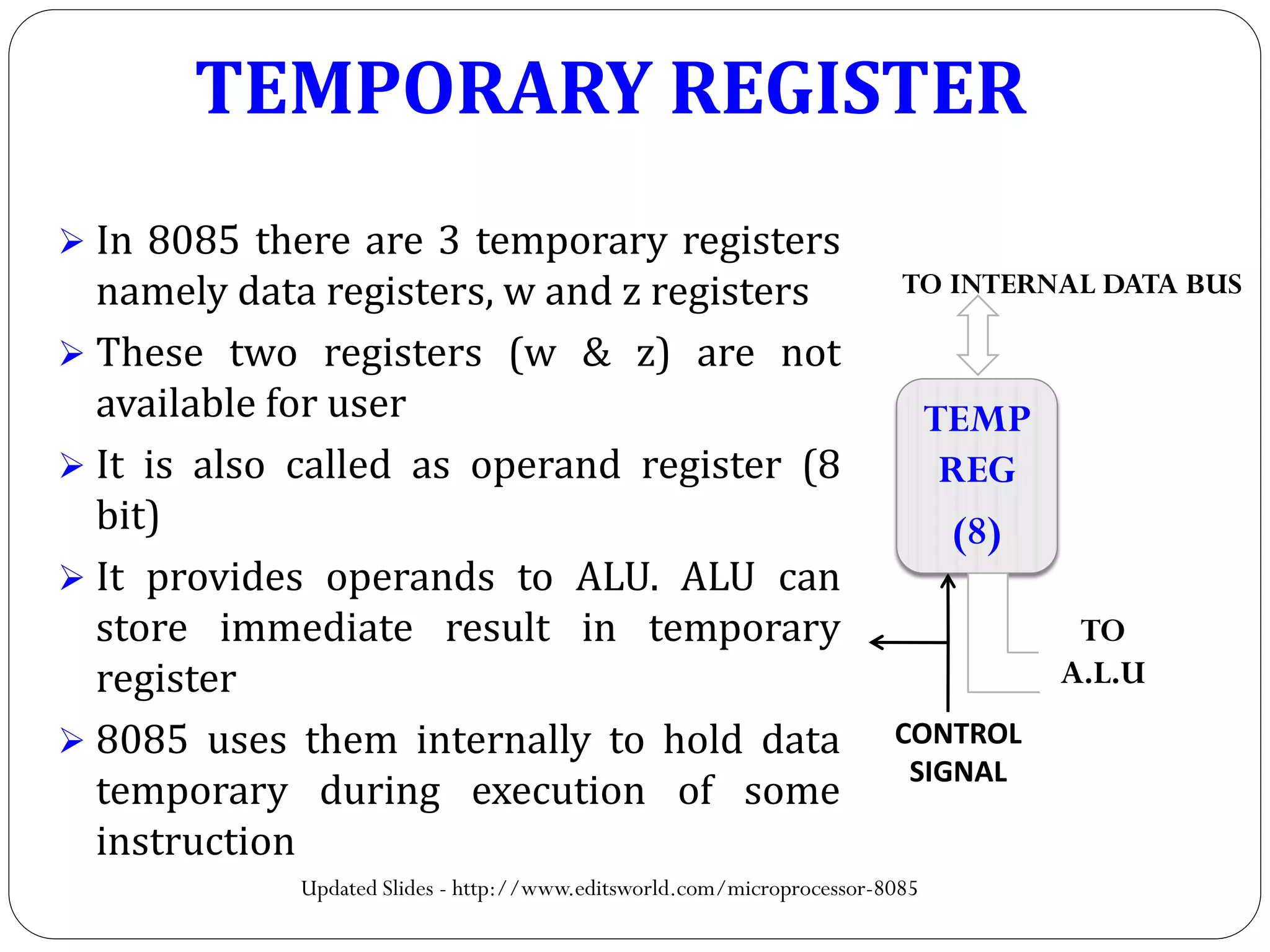
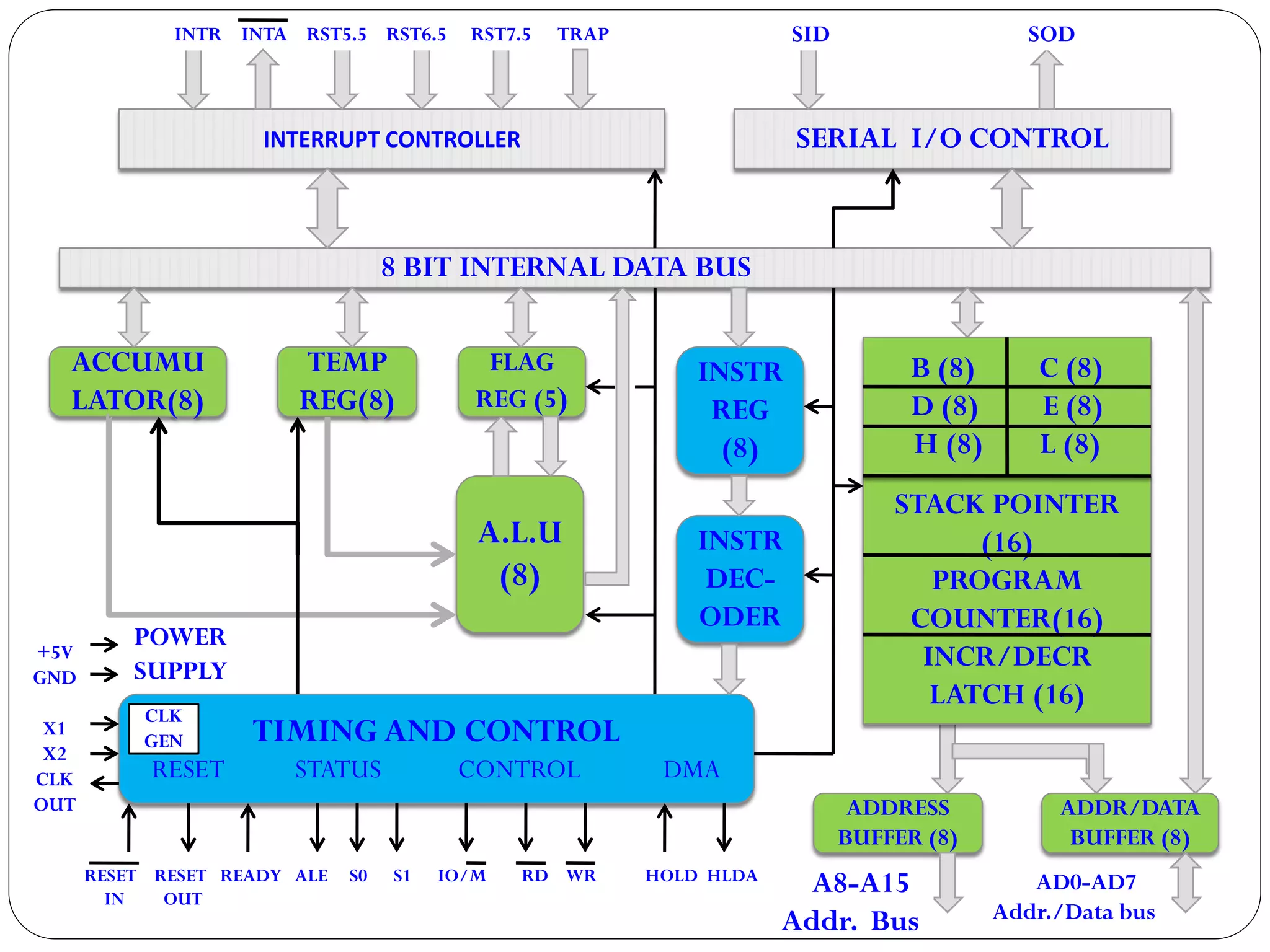
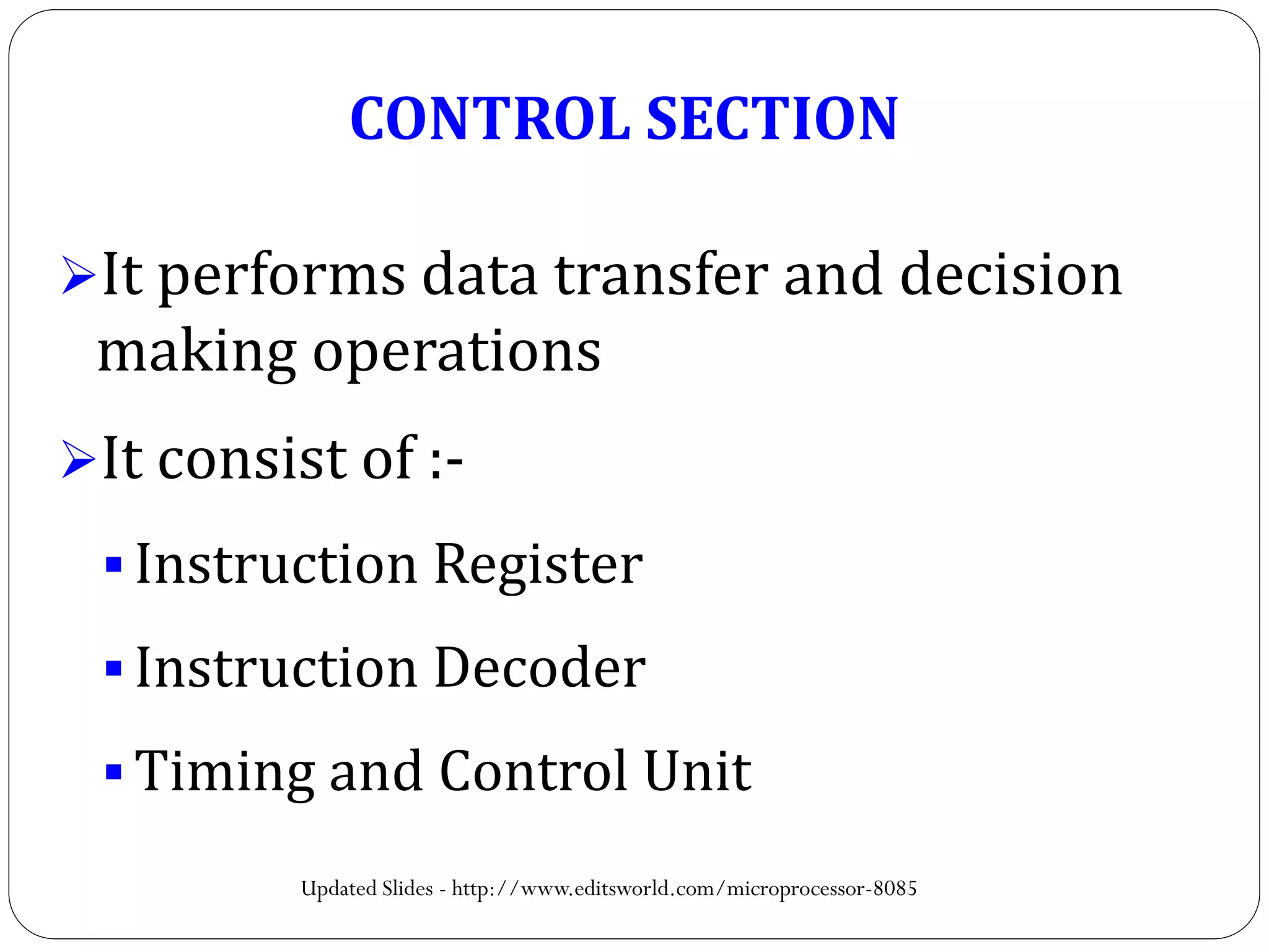
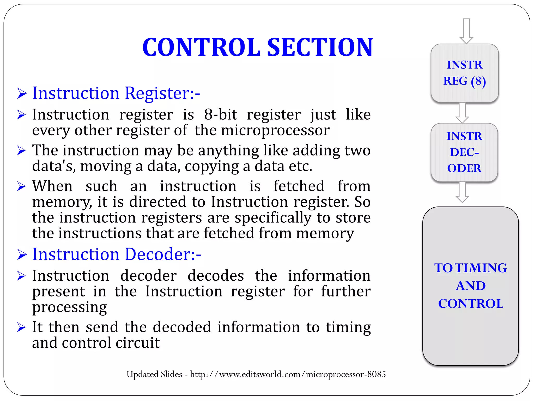
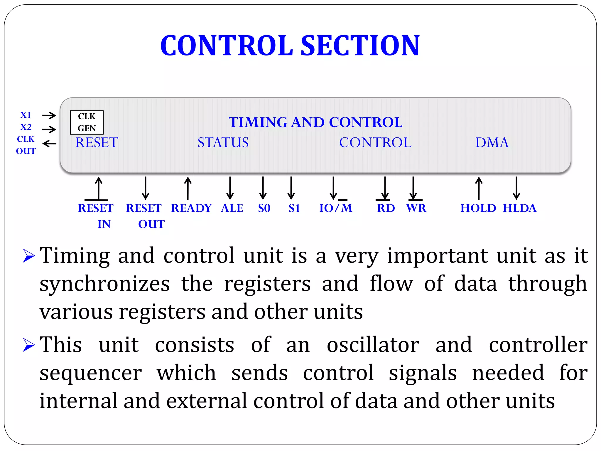
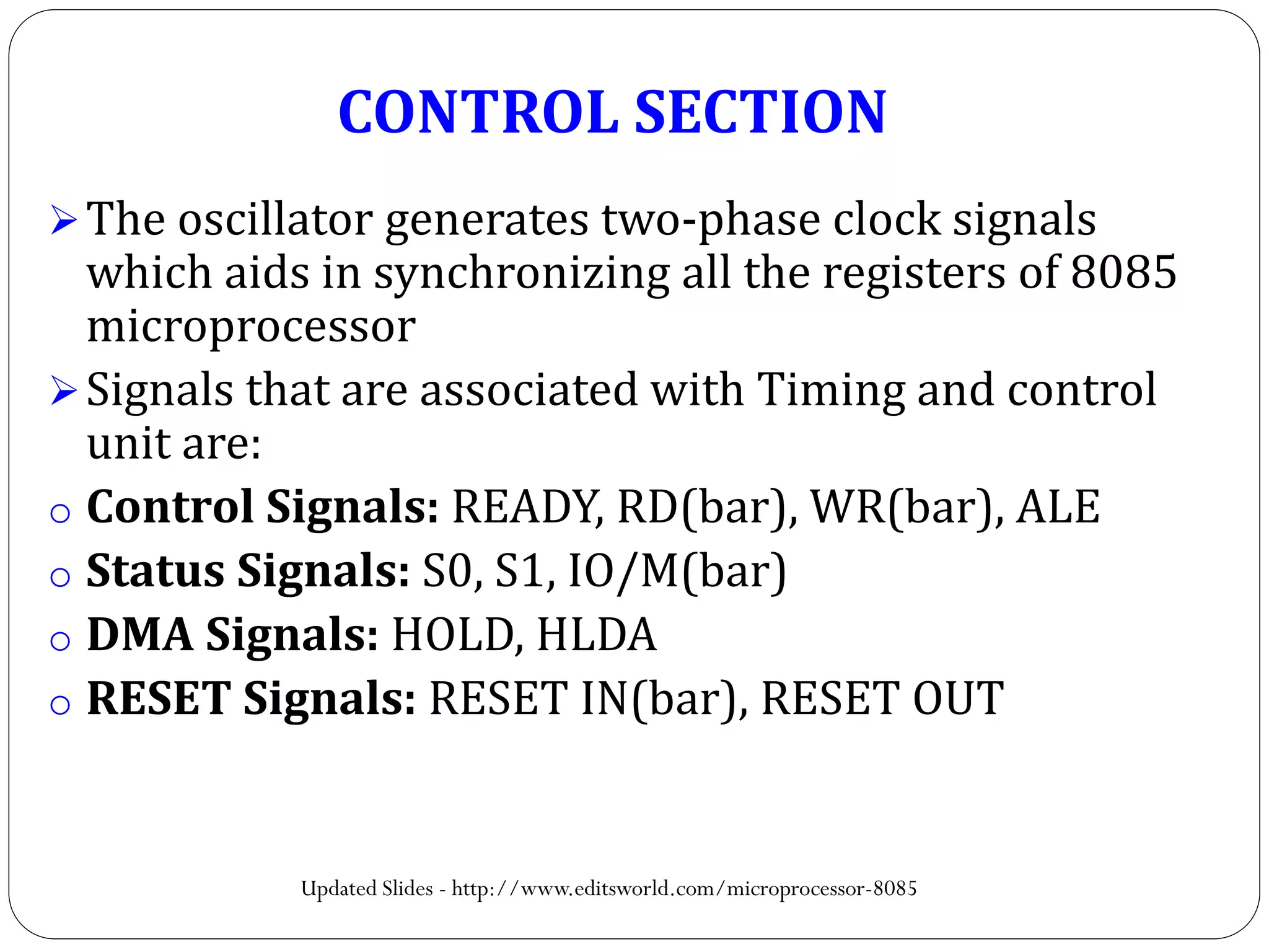
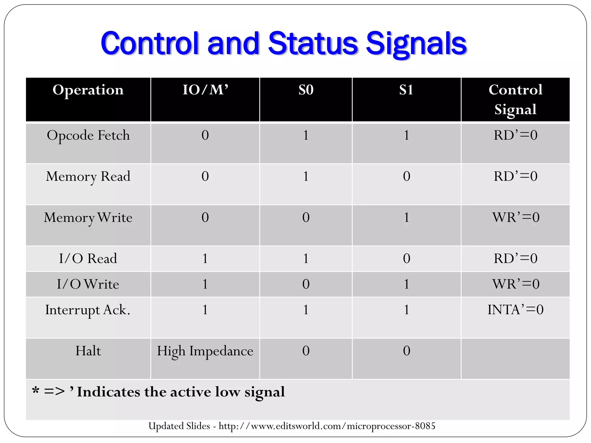
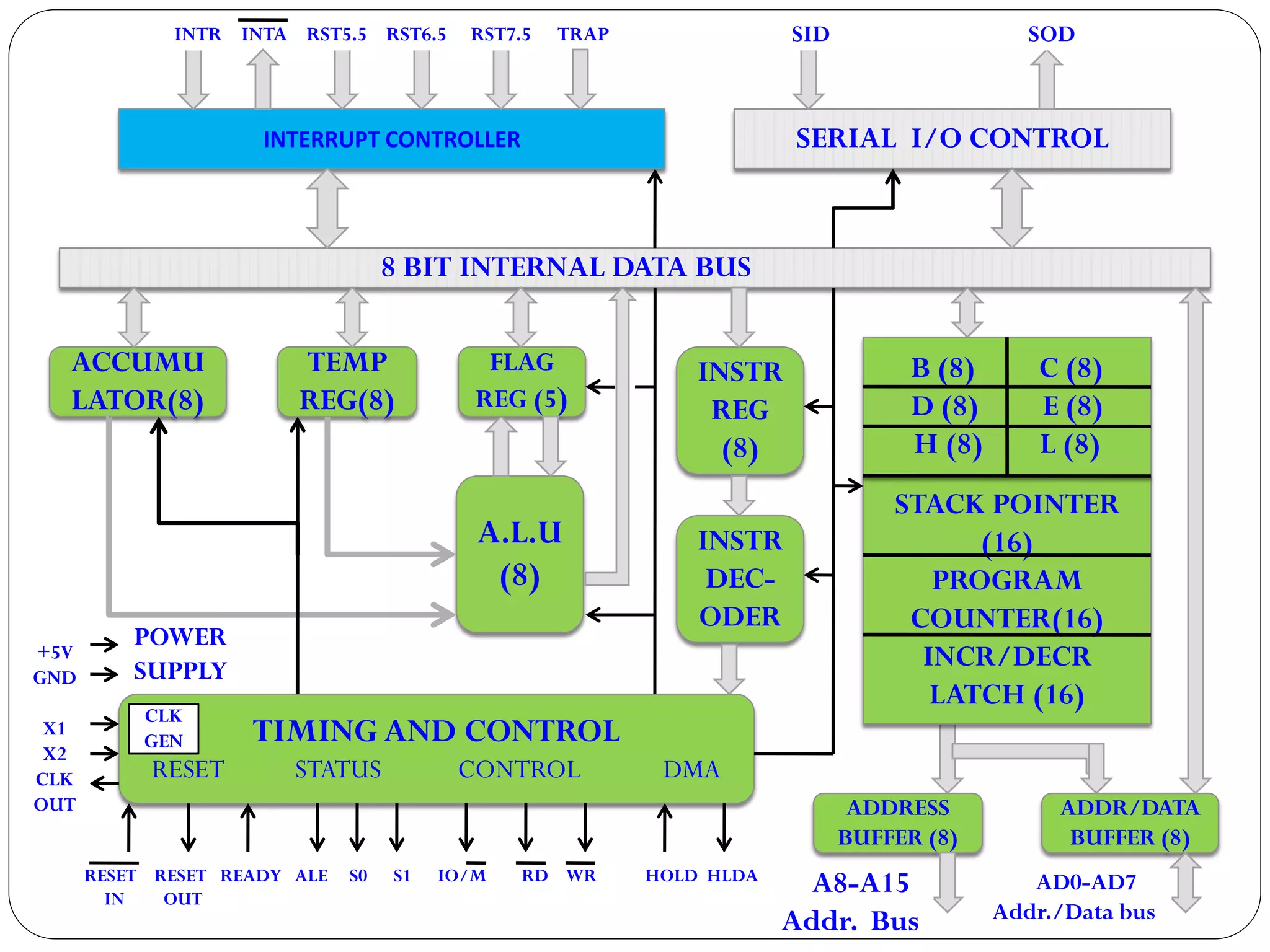
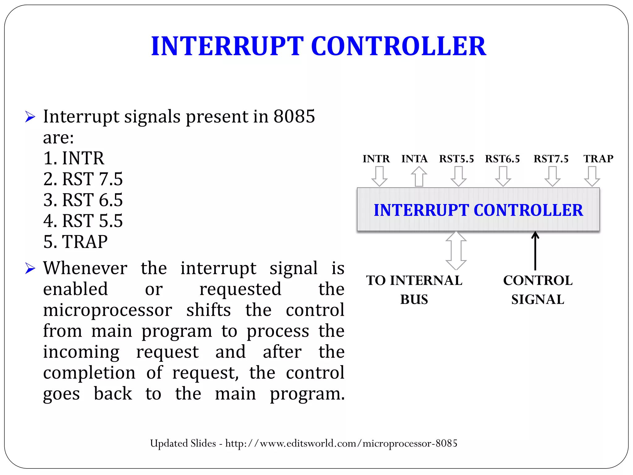
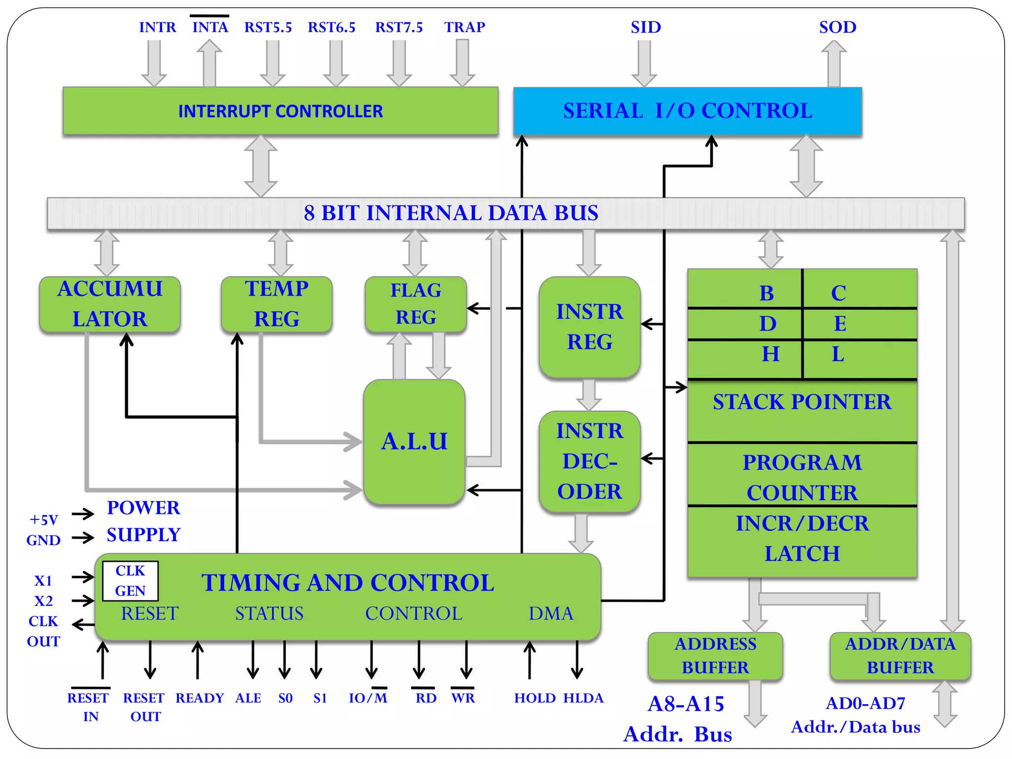
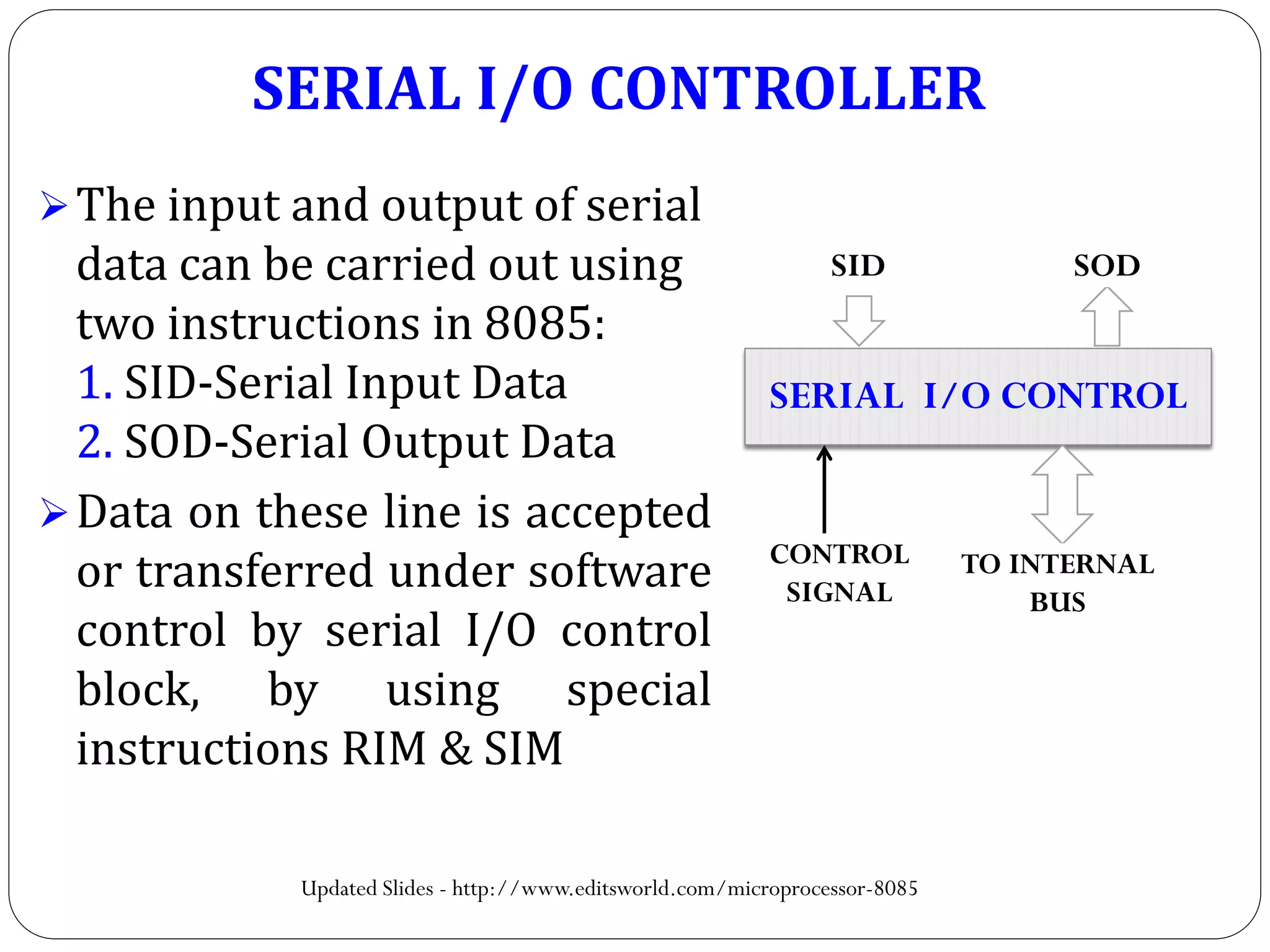
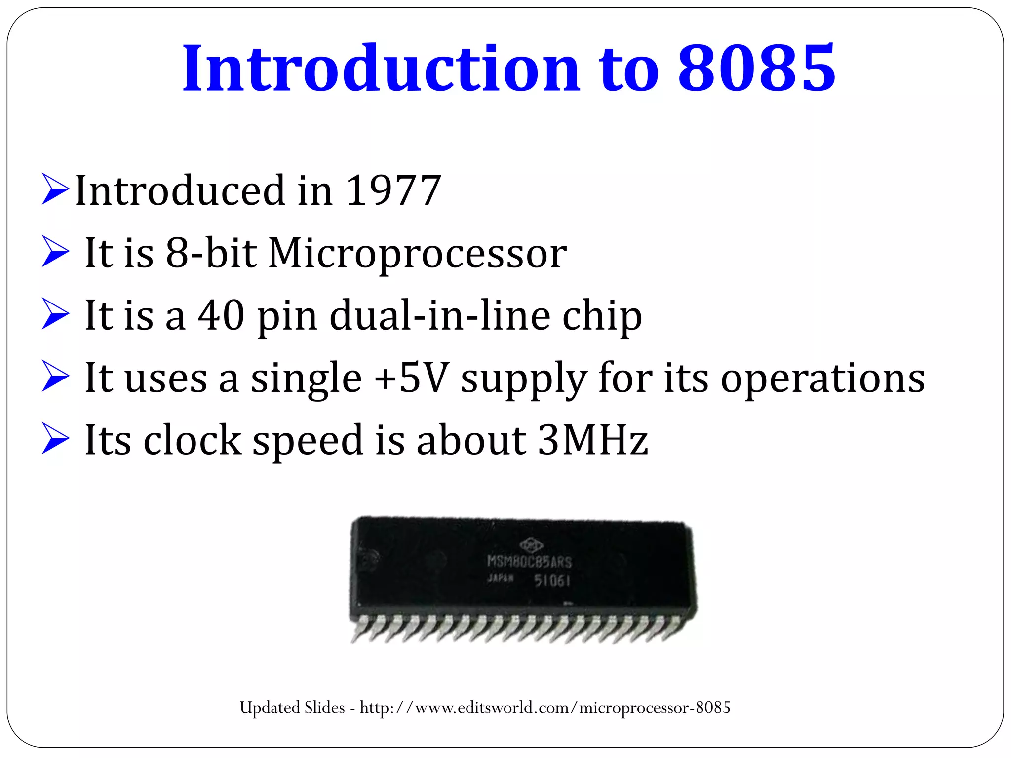
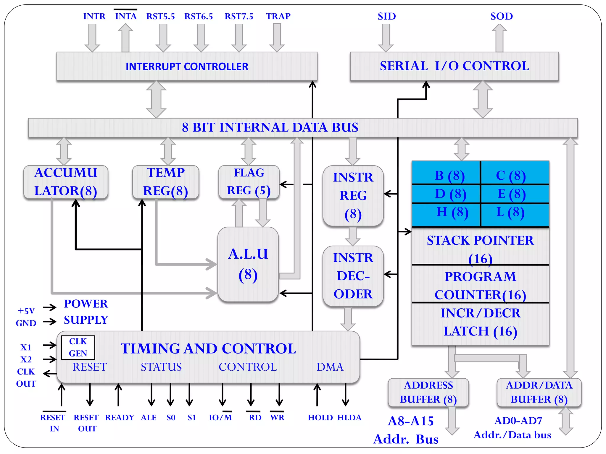
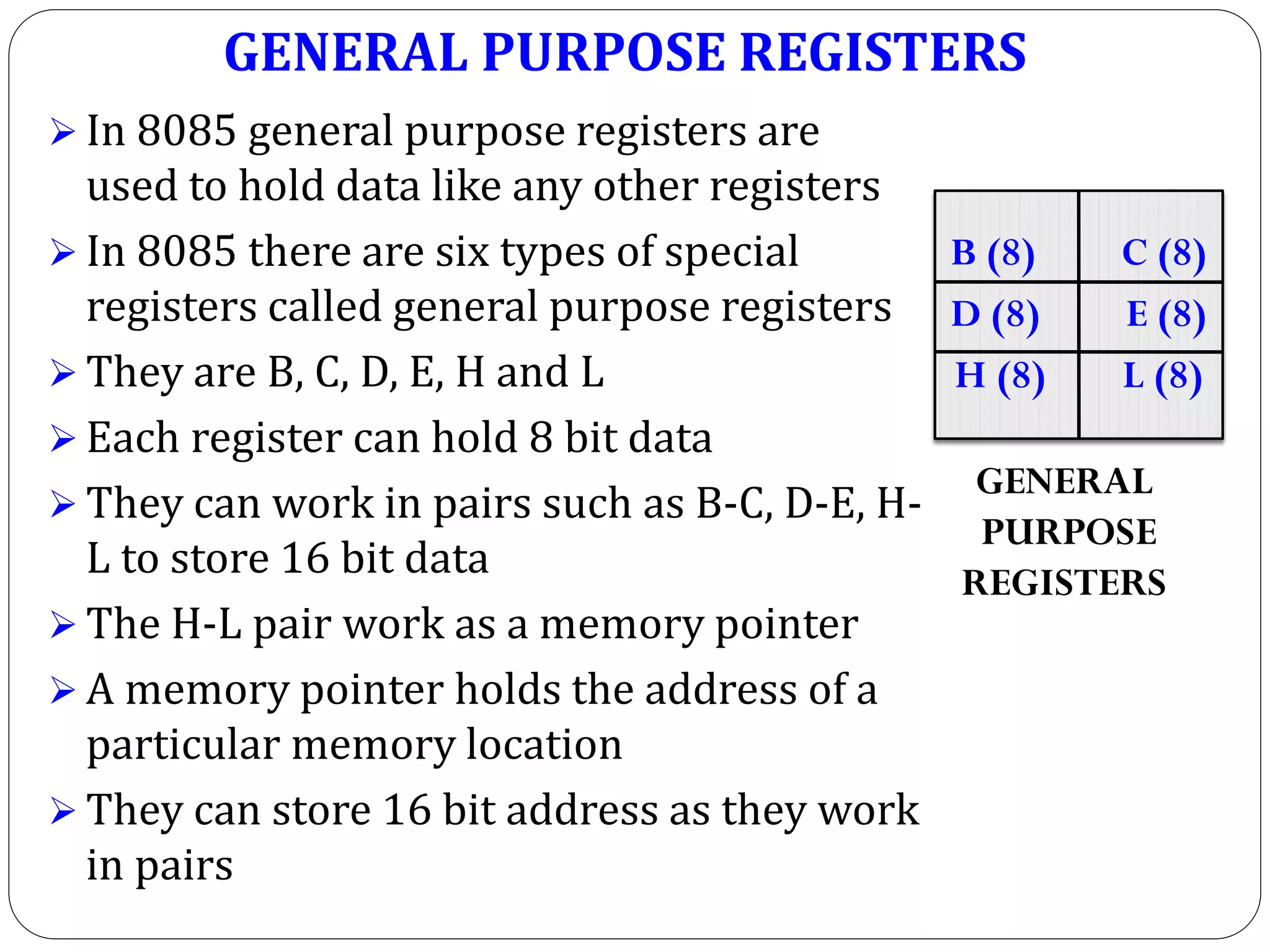
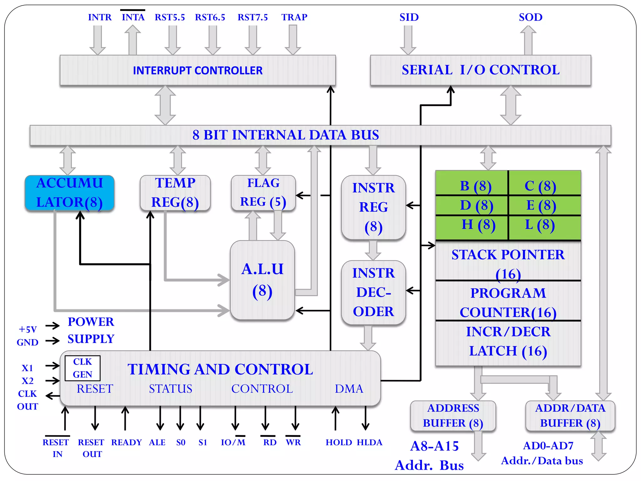
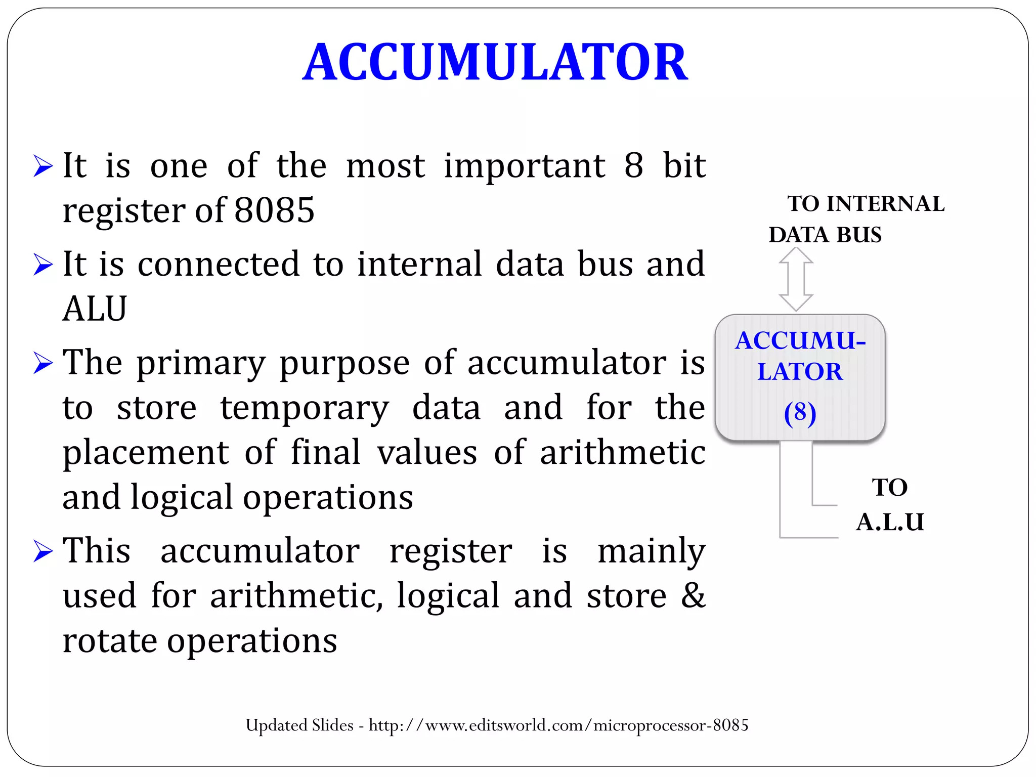
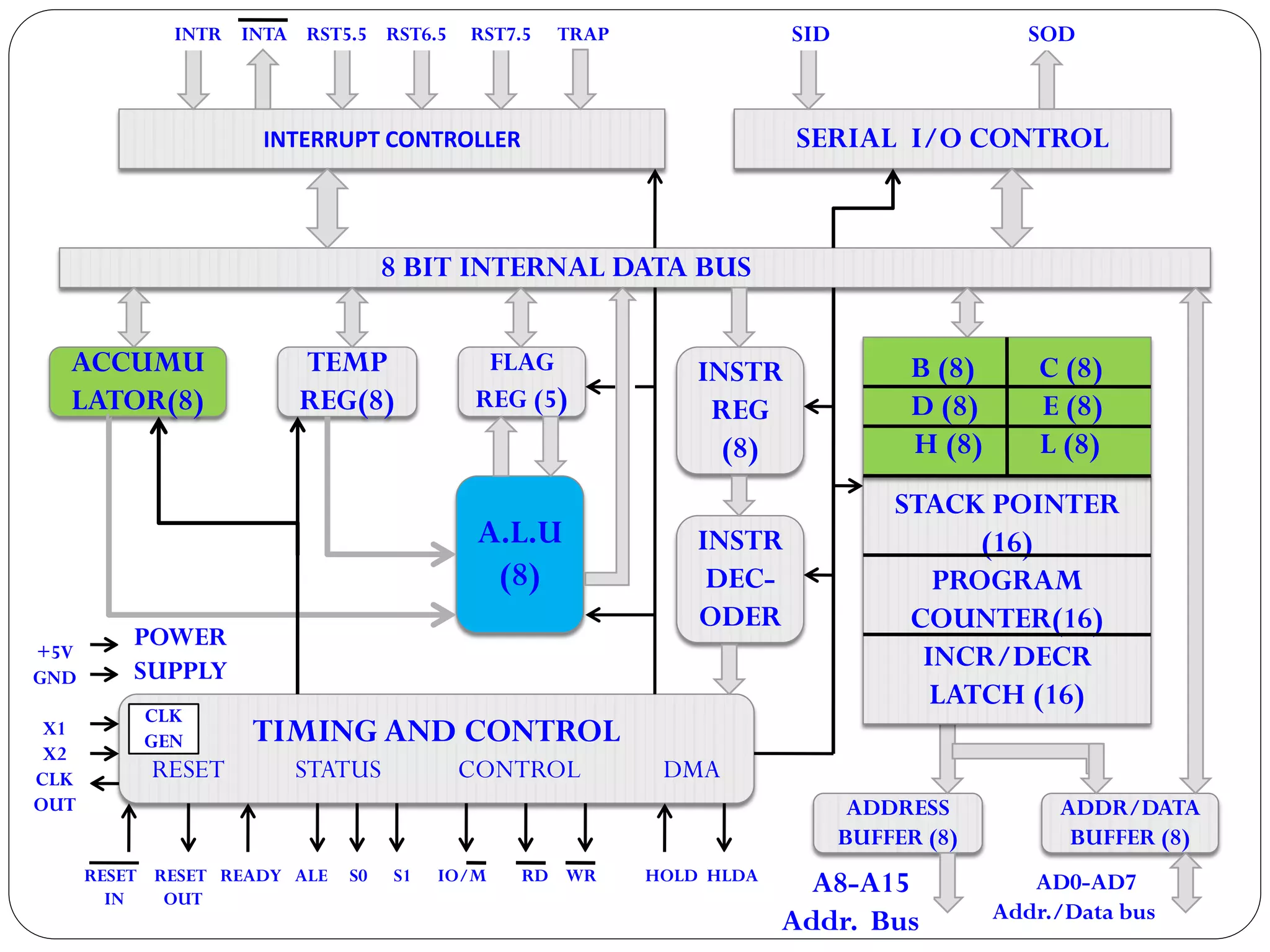
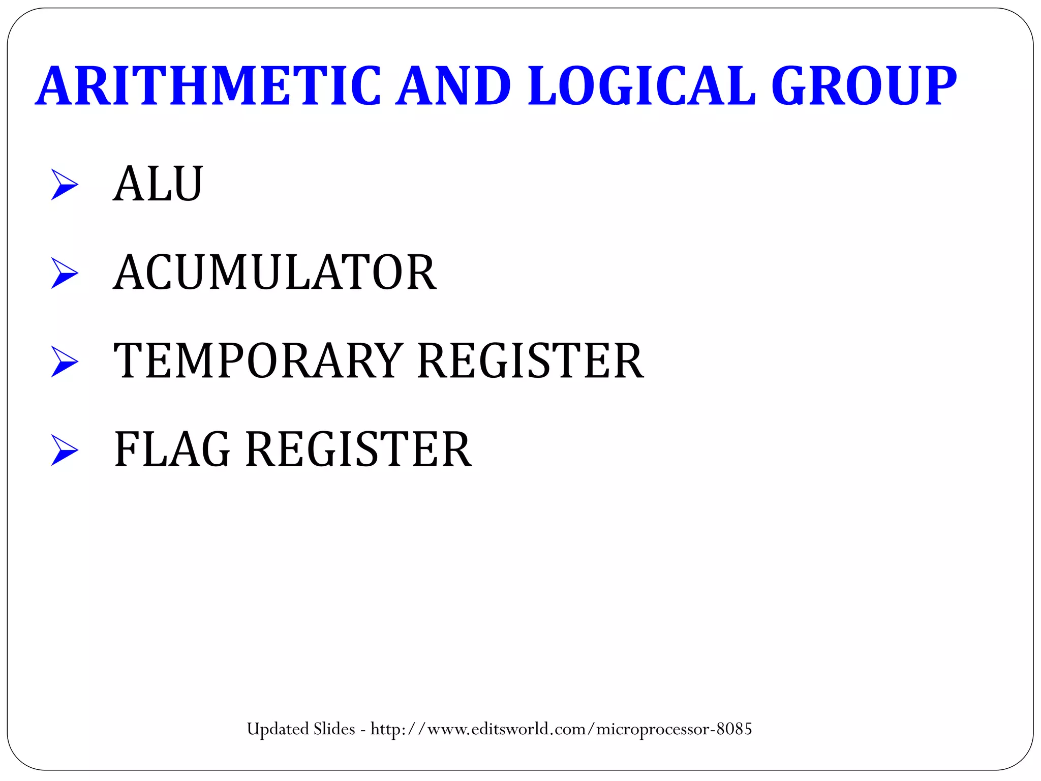
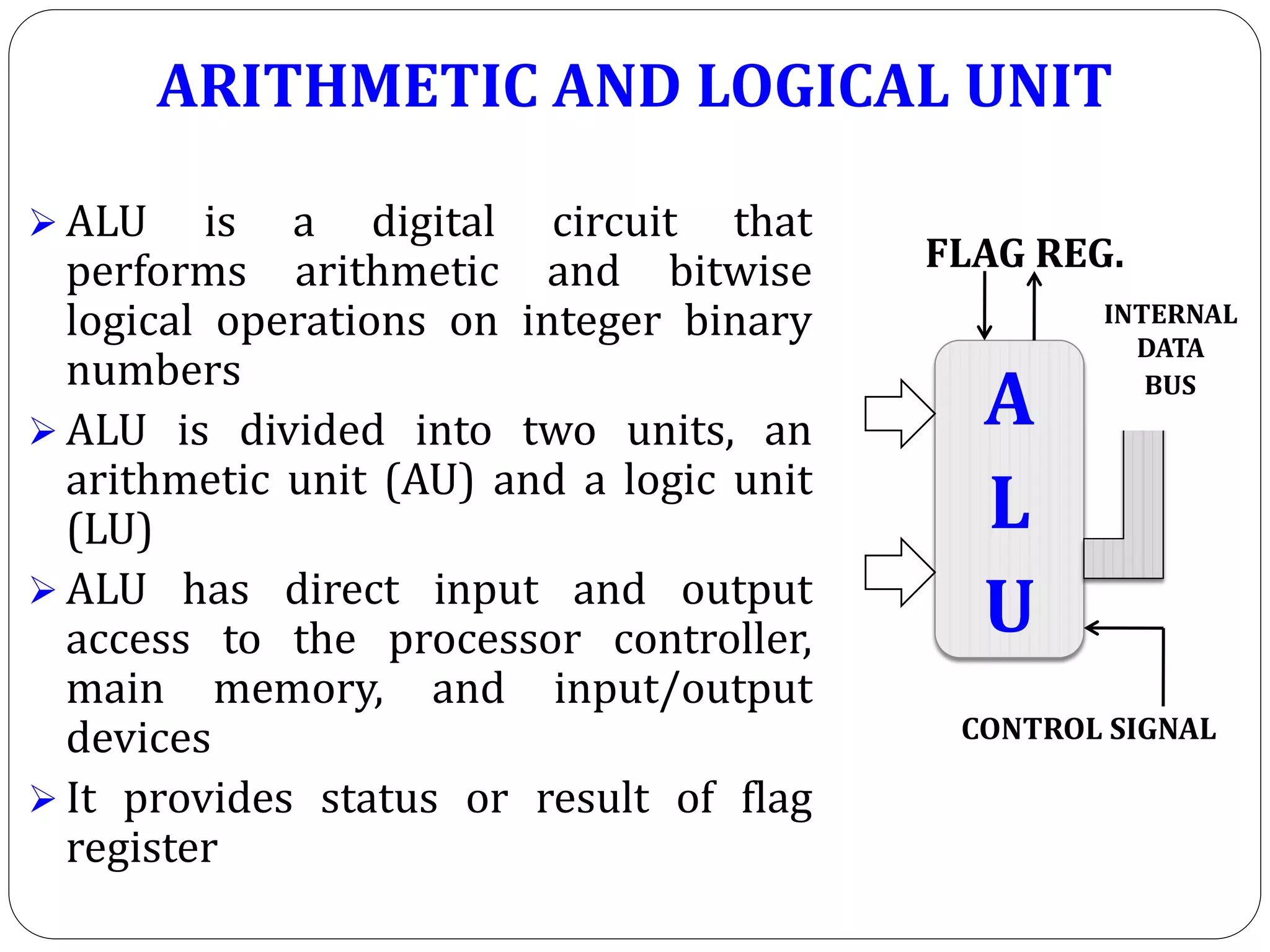
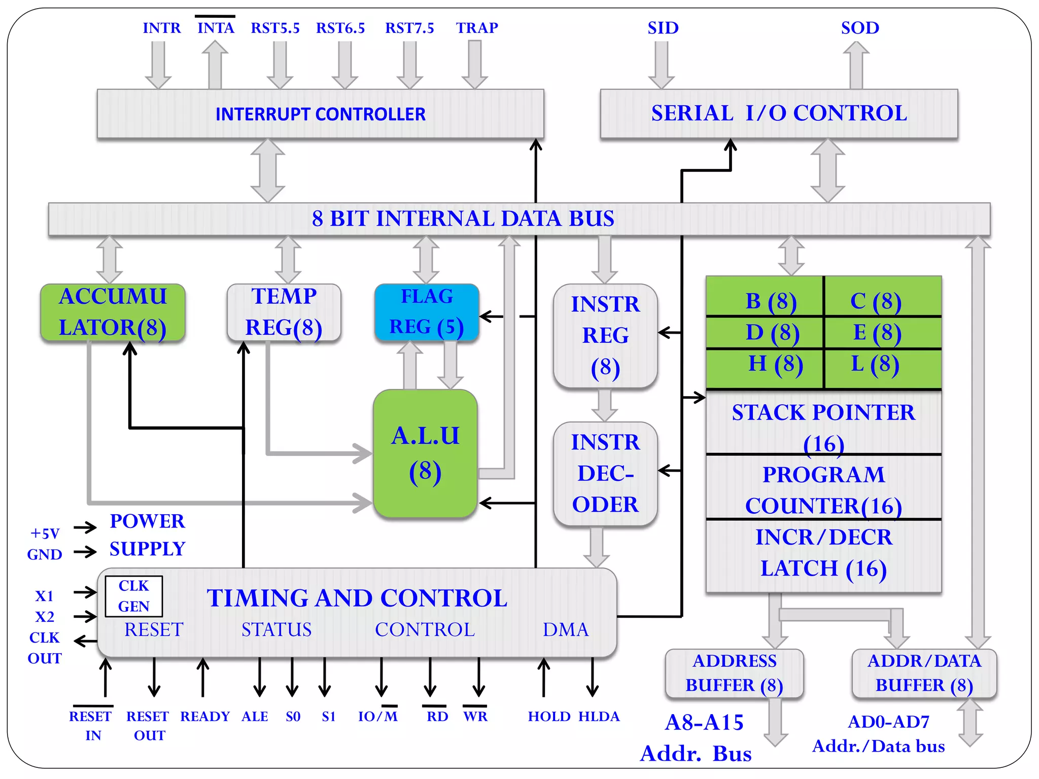
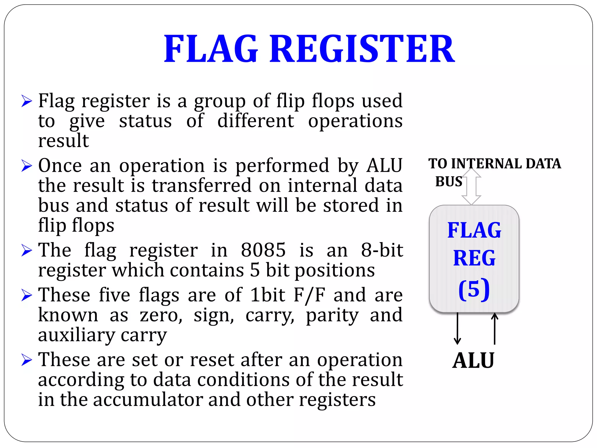
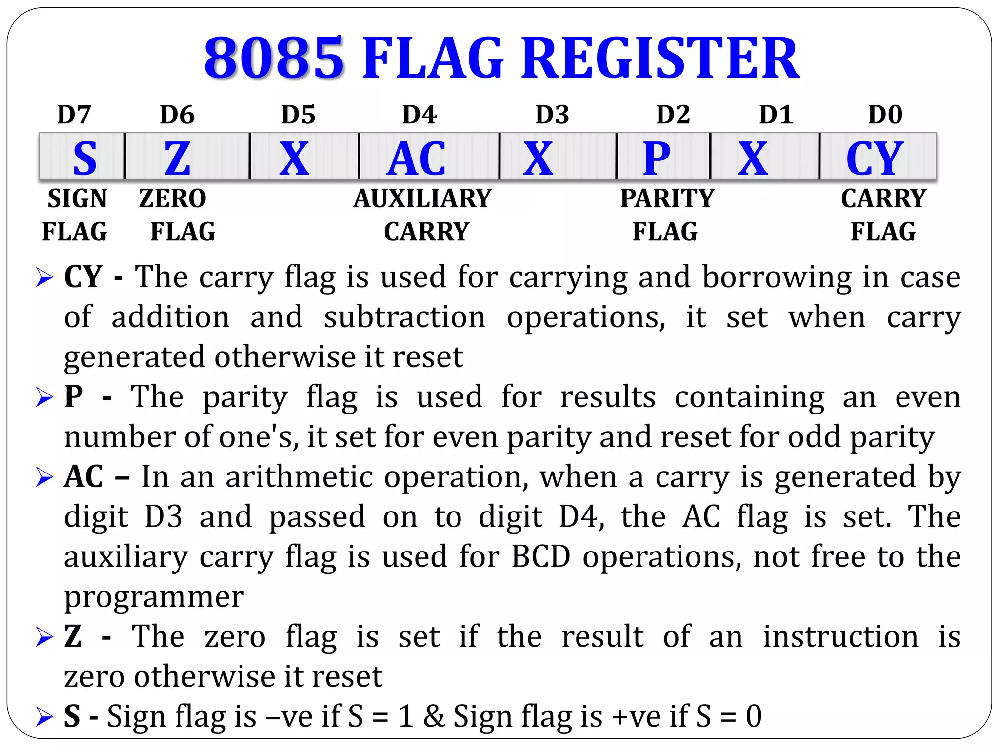
By-
Dileep Kumar Tiwari, Uday Kumar,
Shubham Gupta, Neeti Srivastav
Architecture of 8085
Microprocessor
Introduction to 8085
Introduced in 1977
 It is 8-bit Microprocessor
 It is a 40 pin dual-in-line chip
 It uses a single +5V supply for its operations
 Its clock speed is about 3MHz
Updated Slides - http://www.editsworld.com/microprocessor-8085
Parts of 8085 Microprocessor
Arithmetic and Logical group
Register group
Interrupt control group
Serial I/O control group
Instruction register , decoder, timing
and control group
Updated Slides - http://www.editsworld.com/microprocessor-8085
INTERRUPT CONTROLLER
8 BIT INTERNAL DATA BUS
SERIAL I/O CONTROL
ACCUMU
LATOR(8)
TEMP
REG(8)
FLAG
REG (5)
INSTR
REG
(8)
A.L.U
(8)
TIMING AND CONTROL
RESET STATUS CONTROL DMA
ADDRESS
BUFFER (8)
ADDR/DATA
BUFFER (8)
INSTR
DEC-
ODER
INTR INTA RST5.5 RST6.5 RST7.5 TRAP SID SOD
A8-A15
Addr. Bus
AD0-AD7
Addr./Data bus
RESET RESET READY ALE S0 S1 IO/M RD WR HOLD HLDA
IN OUT
+5V
GND
X1
X2
CLK
OUT
POWER
SUPPLY
CLK
GEN
STACK POINTER
(16)
PROGRAM
COUNTER(16)
INCR/DECR
LATCH (16)
B (8) C (8)
D (8) E (8)
H (8) L (8)
GENERAL PURPOSE REGISTERS
 In 8085 general purpose registers are
used to hold data like any other registers
 In 8085 there are six types of special
registers called general purpose registers
 They are B, C, D, E, H and L
 Each register can hold 8 bit data
 They can work in pairs such as B-C, D-E, H-
L to store 16 bit data
 The H-L pair work as a memory pointer
 A memory pointer holds the address of a
particular memory location
 They can store 16 bit address as they work
in pairs
B (8) C (8)
D (8) E (8)
H (8) L (8)
GENERAL
PURPOSE
REGISTERS
INTERRUPT CONTROLLER
8 BIT INTERNAL DATA BUS
SERIAL I/O CONTROL
ACCUMU
LATOR(8)
TEMP
REG(8)
FLAG
REG (5)
INSTR
REG
(8)
A.L.U
(8)
TIMING AND CONTROL
RESET STATUS CONTROL DMA
ADDRESS
BUFFER (8)
ADDR/DATA
BUFFER (8)
INSTR
DEC-
ODER
INTR INTA RST5.5 RST6.5 RST7.5 TRAP SID SOD
A8-A15
Addr. Bus
AD0-AD7
Addr./Data bus
RESET RESET READY ALE S0 S1 IO/M RD WR HOLD HLDA
IN OUT
+5V
GND
X1
X2
CLK
OUT
POWER
SUPPLY
CLK
GEN
STACK POINTER
(16)
PROGRAM
COUNTER(16)
INCR/DECR
LATCH (16)
B (8) C (8)
D (8) E (8)
H (8) L (8)
ACCUMULATOR
 It is one of the most important 8 bit
register of 8085
 It is connected to internal data bus and
ALU
 The primary purpose of accumulator is
to store temporary data and for the
placement of final values of arithmetic
and logical operations
 This accumulator register is mainly
used for arithmetic, logical and store &
rotate operations
ACCUMU-
LATOR
(8)
TO INTERNAL
DATA BUS
TO
A.L.U
Updated Slides - http://www.editsworld.com/microprocessor-8085
INTERRUPT CONTROLLER
8 BIT INTERNAL DATA BUS
SERIAL I/O CONTROL
ACCUMU
LATOR(8)
TEMP
REG(8)
FLAG
REG (5)
INSTR
REG
(8)
A.L.U
(8)
TIMING AND CONTROL
RESET STATUS CONTROL DMA
ADDRESS
BUFFER (8)
ADDR/DATA
BUFFER (8)
INSTR
DEC-
ODER
INTR INTA RST5.5 RST6.5 RST7.5 TRAP SID SOD
A8-A15
Addr. Bus
AD0-AD7
Addr./Data bus
RESET RESET READY ALE S0 S1 IO/M RD WR HOLD HLDA
IN OUT
+5V
GND
X1
X2
CLK
OUT
POWER
SUPPLY
CLK
GEN
STACK POINTER
(16)
PROGRAM
COUNTER(16)
INCR/DECR
LATCH (16)
B (8) C (8)
D (8) E (8)
H (8) L (8)
ARITHMETIC AND LOGICAL GROUP
 ALU
 ACUMULATOR
 TEMPORARY REGISTER
 FLAG REGISTER
Updated Slides - http://www.editsworld.com/microprocessor-8085
ARITHMETIC AND LOGICAL UNIT
 ALU is a digital circuit that
performs arithmetic and bitwise
logical operations on integer binary
numbers
 ALU is divided into two units, an
arithmetic unit (AU) and a logic unit
(LU)
 ALU has direct input and output
access to the processor controller,
main memory, and input/output
devices
 It provides status or result of flag
register
A
L
U
FLAG REG.
INTERNAL
DATA
BUS
CONTROL SIGNAL
INTERRUPT CONTROLLER
8 BIT INTERNAL DATA BUS
SERIAL I/O CONTROL
ACCUMU
LATOR(8)
TEMP
REG(8)
FLAG
REG (5)
INSTR
REG
(8)
A.L.U
(8)
TIMING AND CONTROL
RESET STATUS CONTROL DMA
ADDRESS
BUFFER (8)
ADDR/DATA
BUFFER (8)
INSTR
DEC-
ODER
INTR INTA RST5.5 RST6.5 RST7.5 TRAP SID SOD
A8-A15
Addr. Bus
AD0-AD7
Addr./Data bus
RESET RESET READY ALE S0 S1 IO/M RD WR HOLD HLDA
IN OUT
+5V
GND
X1
X2
CLK
OUT
POWER
SUPPLY
CLK
GEN
STACK POINTER
(16)
PROGRAM
COUNTER(16)
INCR/DECR
LATCH (16)
B (8) C (8)
D (8) E (8)
H (8) L (8)
FLAG REGISTER
 Flag register is a group of flip flops used
to give status of different operations
result
 Once an operation is performed by ALU
the result is transferred on internal data
bus and status of result will be stored in
flip flops
 The flag register in 8085 is an 8-bit
register which contains 5 bit positions
 These five flags are of 1bit F/F and are
known as zero, sign, carry, parity and
auxiliary carry
 These are set or reset after an operation
according to data conditions of the result
in the accumulator and other registers
FLAG
REG
(5)
TO INTERNAL DATA
BUS
ALU
8085 FLAG REGISTER
 CY - The carry flag is used for carrying and borrowing in case
of addition and subtraction operations, it set when carry
generated otherwise it reset
 P - The parity flag is used for results containing an even
number of one's, it set for even parity and reset for odd parity
 AC – In an arithmetic operation, when a carry is generated by
digit D3 and passed on to digit D4, the AC flag is set. The
auxiliary carry flag is used for BCD operations, not free to the
programmer
 Z - The zero flag is set if the result of an instruction is
zero otherwise it reset
 S - Sign flag is –ve if S = 1 & Sign flag is +ve if S = 0
S Z X AC X P X CY
D7 D6 D5 D4 D3 D2 D1 D0
SIGN ZERO AUXILIARY PARITY CARRY
FLAG FLAG CARRY FLAG FLAG
(Carry) 10 0 10
D7 D6 D5 D4 D3 D2 D1 D0
[A] 0 1 1 1 0 0 0 1
[B] 1 0 1 0 1 0 0 1
1 1 0 0 1 0 0 0 (RESULT)
MSB LSB
AC=1,In an airithmetic operation D3 bit borrow
a carry from D4 bit. So the auxiliary flag is set.
EXAMPLE OF AUXILIARY FLAG
MVI B, A9H
MVI C, 71H
MOV A,C
SBB B
HLT
EXAMPLE OF ZERO FLAG
Z=1,The Zero flag is set because the ALU
operation result in 0
MVI A,25H
XRA A
HLT
(XOR A register with Accumulator)
D7 D6 D5 D4 D3 D2 D1D0
0 0 1 0 0 1 0 1
0 0 1 0 0 1 0 1
0 0 0 0 0 0 0 0
Updated Slides - http://www.editsworld.com/microprocessor-8085
P=1, After an arithmetic and logic operation the result
has an even number of 1s,the Parity flag is set
EXAMPLE OF PARITY FLAG
MVI A,71
ANA A
HLT
( AND A register with Accumulator)
D7 D6 D5 D4 D3 D2 D1 D0
0 1 1 1 0 0 0 1
0 1 1 1 0 0 0 1
0 1 1 1 0 0 0 1
Updated Slides - http://www.editsworld.com/microprocessor-8085
EXAMPLE OF CARRY FLAG
CY=1, After ALU operation D7 bit of the result
generate carry (bit no nine is 1), the Carry flag is set
D7 D6 D5 D4 D3 D2 D1 D0
1 1 1 1 0 0 0 0
0 1 1 1 1 0 0 0
Carry 1 0 0 0 0 1 0 0 0
MVI A,F2H
MVI B,7AH
ADD B
HLT
Updated Slides - http://www.editsworld.com/microprocessor-8085
EXAMPLE OF SIGN FLAG
D7 D6 D5 D4 D3 D2 D1D0
0 0 1 0 0 0 0 0
1 0 0 0 0 0 0 0
1 0 1 0 0 0 0 0
MVI A,20H
MVI B,80H
ADD B
1
S=1, After an ALU operation,D7 bit of the result is 1,the Sign
flag is set. Sign bit 1 indicates the result is negative;
otherwise it is positive
Updated Slides - http://www.editsworld.com/microprocessor-8085
USE OF ALL FLAG
 CY=1 - D7 bit of the result generate carry (bit number nine is1), so the
Carry flag is set
 S=0 - Result of arithmetic operation is positive so the sign bit is zero
 P=1 -The result has an even number of 1s,the Parity flag is set
 AC=0 -The carry is not generated by digit D3, so the auxiliary flag is reset
 Z=0 -TheALU operation result is not 0. So the zero flag is reset
MVI A, f2H
MVI B, 7AH
ADD B
HLT
D7 D6 D5 D4 D3 D2 D1D0
1 1 1 1 0 0 1 0
0 1 1 1 1 0 1 0
0 1 1 0 1 1 0 01
INTERRUPT CONTROLLER
8 BIT INTERNAL DATA BUS
SERIAL I/O CONTROL
ACCUMU
LATOR(8)
TEMP
REG(8)
FLAG
REG (5)
INSTR
REG
(8)
A.L.U
(8)
TIMING AND CONTROL
RESET STATUS CONTROL DMA
ADDRESS
BUFFER (8)
ADDR/DATA
BUFFER (8)
INSTR
DEC-
ODER
INTR INTA RST5.5 RST6.5 RST7.5 TRAP SID SOD
A8-A15
Addr. Bus
AD0-AD7
Addr./Data bus
RESET RESET READY ALE S0 S1 IO/M RD WR HOLD HLDA
IN OUT
+5V
GND
X1
X2
CLK
OUT
POWER
SUPPLY
CLK
GEN
STACK POINTER
(16)
PROGRAM
COUNTER(16)
INCR/DECR
LATCH (16)
B (8) C (8)
D (8) E (8)
H (8) L (8)
SPECIAL PURPOSE REGISTER
 It consists of three 16 bit register:-
Program Counter , Stack pointer,
Incrementer / Decrementer Latch
Program Counter –
Program counter is a special purpose
register. It holds the address of the next
instruction to be executed, in order to
save time
Stack Pointer -
• A stack is nothing but the portion of RAM
• It works on the LIFO concept
• Stack pointer maintains the address of the
last byte that is entered into stack
• Each time when the data is loaded into
stack, Stack pointer gets decremented
STACK POINTER
(16)
PROGRAM COUNTER
(16)
INCR/DECR LATCH (16)
ADDRESS
BUFFER (8)
ADDR/DATA
BUFFER (8)
SPECIAL PURPOSE
REGISTER
Updated Slides - http://www.editsworld.com/microprocessor-8085
INCR/DECR LATCH :-
It is used to increment or decrement the content of
program counter and stack pointer register
 Address /data buffer and address buffer:-
o The contents of the stack pointer and program
counter are loaded into the address buffer and
address-data buffer
o These buffers are then used to drive the external
address bus and address-data bus.
o As the memory and I/O chips are connected to
these buses, the CPU can exchange desired data
to the memory and I/O chips
o The address-data buffer is not only connected to
the external data bus but also to the internal data
bus which consists of 8-bits
o The address data buffer can both send and
receive data from internal data bus
INCR/DECR
LATCH (16)
ADDR/DATA
BUFFER (8)
ADDRESS
BUFFER (8)
A8-A15
Address
Buffer
AD0-AD7
Address/Data
buffer
SPECIAL PURPOSE REGISTER
INTERRUPT CONTROLLER
8 BIT INTERNAL DATA BUS
SERIAL I/O CONTROL
ACCUMU
LATOR(8)
TEMP
REG(8)
FLAG
REG (5)
INSTR
REG
(8)
A.L.U
(8)
TIMING AND CONTROL
RESET STATUS CONTROL DMA
ADDRESS
BUFFER (8)
ADDR/DATA
BUFFER (8)
INSTR
DEC-
ODER
INTR INTA RST5.5 RST6.5 RST7.5 TRAP SID SOD
A8-A15
Addr. Bus
AD0-AD7
Addr./Data bus
RESET RESET READY ALE S0 S1 IO/M RD WR HOLD HLDA
IN OUT
+5V
GND
X1
X2
CLK
OUT
POWER
SUPPLY
CLK
GEN
STACK POINTER
(16)
PROGRAM
COUNTER(16)
INCR/DECR
LATCH (16)
B (8) C (8)
D (8) E (8)
H (8) L (8)
TEMPORARY REGISTER
 In 8085 there are 3 temporary registers
namely data registers, w and z registers
 These two registers (w & z) are not
available for user
 It is also called as operand register (8
bit)
 It provides operands to ALU. ALU can
store immediate result in temporary
register
 8085 uses them internally to hold data
temporary during execution of some
instruction
TEMP
REG
(8)
TO INTERNAL DATA BUS
TO
A.L.U
CONTROL
SIGNAL
Updated Slides - http://www.editsworld.com/microprocessor-8085
INTERRUPT CONTROLLER
8 BIT INTERNAL DATA BUS
SERIAL I/O CONTROL
ACCUMU
LATOR(8)
TEMP
REG(8)
FLAG
REG (5)
INSTR
REG
(8)
A.L.U
(8)
TIMING AND CONTROL
RESET STATUS CONTROL DMA
ADDRESS
BUFFER (8)
ADDR/DATA
BUFFER (8)
INSTR
DEC-
ODER
INTR INTA RST5.5 RST6.5 RST7.5 TRAP SID SOD
A8-A15
Addr. Bus
AD0-AD7
Addr./Data bus
RESET RESET READY ALE S0 S1 IO/M RD WR HOLD HLDA
IN OUT
+5V
GND
X1
X2
CLK
OUT
POWER
SUPPLY
CLK
GEN
STACK POINTER
(16)
PROGRAM
COUNTER(16)
INCR/DECR
LATCH (16)
B (8) C (8)
D (8) E (8)
H (8) L (8)
CONTROL SECTION
It performs data transfer and decision
making operations
It consist of :-
 Instruction Register
 Instruction Decoder
 Timing and Control Unit
Updated Slides - http://www.editsworld.com/microprocessor-8085
 Instruction Register:-
 Instruction register is 8-bit register just like
every other register of the microprocessor
 The instruction may be anything like adding two
data's, moving a data, copying a data etc.
 When such an instruction is fetched from
memory, it is directed to Instruction register. So
the instruction registers are specifically to store
the instructions that are fetched from memory
 Instruction Decoder:-
 Instruction decoder decodes the information
present in the Instruction register for further
processing
 It then send the decoded information to timing
and control circuit
INSTR
REG (8)
INSTR
DEC-
ODER
TOTIMING
AND
CONTROL
CONTROL SECTION
Updated Slides - http://www.editsworld.com/microprocessor-8085
Timing and control unit is a very important unit as it
synchronizes the registers and flow of data through
various registers and other units
This unit consists of an oscillator and controller
sequencer which sends control signals needed for
internal and external control of data and other units
TIMING AND CONTROL
RESET STATUS CONTROL DMA
CLK
GEN
X1
X2
CLK
OUT
RESET RESET READY ALE S0 S1 IO/M RD WR HOLD HLDA
IN OUT
CONTROL SECTION
The oscillator generates two-phase clock signals
which aids in synchronizing all the registers of 8085
microprocessor
Signals that are associated with Timing and control
unit are:
o Control Signals: READY, RD(bar), WR(bar), ALE
o Status Signals: S0, S1, IO/M(bar)
o DMA Signals: HOLD, HLDA
o RESET Signals: RESET IN(bar), RESET OUT
CONTROL SECTION
Updated Slides - http://www.editsworld.com/microprocessor-8085
Control and Status Signals
Signals:
 RD – Read (active low). To indicate that the I/O or
memory selected is to be read and data are available on
the bus.
 WR – Write: Active low. This is to indicate that the data
available on the bus are to be written to memory or I/O
ports.
 IO/M – To differentiate I/O operation of memory
operations.
• ‘0’ - indicates a memory operation.
• ‘1’-indicates an I/O operation.
 IO/M combined with RD and WR to generate I/O and
memory control signals.
 S1 and S0: Status signals, similar to IO/M, can identify
various operations as shown on the following table :
Control and Status Signals
Operation IO/M’ S0 S1 Control
Signal
Opcode Fetch 0 1 1 RD’=0
Memory Read 0 1 0 RD’=0
MemoryWrite 0 0 1 WR’=0
I/O Read 1 1 0 RD’=0
I/OWrite 1 0 1 WR’=0
Interrupt Ack. 1 1 1 INTA’=0
Halt High Impedance 0 0
* => ’ Indicates the active low signal
Updated Slides - http://www.editsworld.com/microprocessor-8085
INTERRUPT CONTROLLER
8 BIT INTERNAL DATA BUS
SERIAL I/O CONTROL
ACCUMU
LATOR(8)
TEMP
REG(8)
FLAG
REG (5)
INSTR
REG
(8)
A.L.U
(8)
TIMING AND CONTROL
RESET STATUS CONTROL DMA
ADDRESS
BUFFER (8)
ADDR/DATA
BUFFER (8)
INSTR
DEC-
ODER
INTR INTA RST5.5 RST6.5 RST7.5 TRAP SID SOD
A8-A15
Addr. Bus
AD0-AD7
Addr./Data bus
RESET RESET READY ALE S0 S1 IO/M RD WR HOLD HLDA
IN OUT
+5V
GND
X1
X2
CLK
OUT
POWER
SUPPLY
CLK
GEN
STACK POINTER
(16)
PROGRAM
COUNTER(16)
INCR/DECR
LATCH (16)
B (8) C (8)
D (8) E (8)
H (8) L (8)
INTERRUPT CONTROLLER
 Interrupt signals present in 8085
are:
1. INTR
2. RST 7.5
3. RST 6.5
4. RST 5.5
5. TRAP
 Whenever the interrupt signal is
enabled or requested the
microprocessor shifts the control
from main program to process the
incoming request and after the
completion of request, the control
goes back to the main program.
INTERRUPT CONTROLLER
INTR INTA RST5.5 RST6.5 RST7.5 TRAP
TO INTERNAL
BUS
CONTROL
SIGNAL
Updated Slides - http://www.editsworld.com/microprocessor-8085
 Of the four interrupts TRAP is a NON-MASKABLE interrupt
control and other three are maskable interrupts.
 A non-maskable interrupt is an interrupt which is given the
highest priority in the order of interrupts.
 Suppose you want an instruction to be processed
immediately, then you can give the instruction as a non-
maskable interrupt.
 Further the non-maskable interrupt cannot be disabled by
programmer at any point of time.
 Whereas the maskable interrupts can be disabled and
enabled using EI and DI instructions.
 Among the maskable interrupts RST 7.5 is given the highest
priority above RST 6.5 and least priority is given to INTR.
INTERRUPT CONTROLLER
Updated Slides - http://www.editsworld.com/microprocessor-8085
An interrupt is a hardware-initiated subroutine CALL. When
interrupt pin is activated, an ISR will be called interrupting the
program that is currently executing
INTERRUPT SIGNALS
PIN Subroutine Location
TRAP 0024
RST 5.5 002C
RST 6.5 0034
RST 7.5 003C
FIND THE INTERRUPT X8 IN ALL MASK
 TRAP>RST7.5>RST 6.5>RST 5.5
 TRAP is also called RST 4.5.This is nonmaskable interrupt and has the
highest priority
RST7.5, 6.5, 5.5 - Restart interrupt: These are vectored
interrupts that transfer the program control to specific memory
locations. They have higher priorities than the INTR interrupt
among of these three. Because INTR is non vectored it does not
have any address.
 TRAP or RST 4.5 = (4.5*8=36), it convert hexadecimal no.
16 36
2 4 =0024H
Updated Slides - http://www.editsworld.com/microprocessor-8085
 RST 7.5=(7.5*8=60), it convert hexadecimal no.
16 60
3 12 =312H=>003CH
 RST 6.5=(6.5*8=52), it convert hexadecimal no.
16 52
3 4 =0034H
 RST 5.5=(5.5*8=44), it convert hexadecimal no.
16 44
2 12 =212H=>002CH
Updated Slides - http://www.editsworld.com/microprocessor-8085
INTERRUPT CONTROLLER
8 BIT INTERNAL DATA BUS
SERIAL I/O CONTROL
ACCUMU
LATOR
TEMP
REG
FLAG
REG INSTR
REG
A.L.U
TIMING AND CONTROL
RESET STATUS CONTROL DMA
ADDRESS
BUFFER
ADDR/DATA
BUFFER
INSTR
DEC-
ODER
INTR INTA RST5.5 RST6.5 RST7.5 TRAP SID SOD
A8-A15
Addr. Bus
AD0-AD7
Addr./Data bus
RESET RESET READY ALE S0 S1 IO/M RD WR HOLD HLDA
IN OUT
+5V
GND
X1
X2
CLK
OUT
POWER
SUPPLY
CLK
GEN
STACK POINTER
PROGRAM
COUNTER
INCR/DECR
LATCH
B C
D E
H L
SERIAL I/O CONTROLLER
The input and output of serial
data can be carried out using
two instructions in 8085:
1. SID-Serial Input Data
2. SOD-Serial Output Data
Data on these line is accepted
or transferred under software
control by serial I/O control
block, by using special
instructions RIM & SIM
SERIAL I/O CONTROL
SID SOD
TO INTERNAL
BUS
CONTROL
SIGNAL
Updated Slides - http://www.editsworld.com/microprocessor-8085
THANKYOU
For any Query feel free to contact
E-mail – dil.371987@gmail.com
Updated Slides - http://www.editsworld.com/microprocessor-8085

Architecture of 8085

  • 1.
    By- Dileep Kumar Tiwari,Uday Kumar, Shubham Gupta, Neeti Srivastav Architecture of 8085 Microprocessor
  • 2.
    Introduction to 8085 Introducedin 1977  It is 8-bit Microprocessor  It is a 40 pin dual-in-line chip  It uses a single +5V supply for its operations  Its clock speed is about 3MHz Updated Slides - http://www.editsworld.com/microprocessor-8085
  • 3.
    Parts of 8085Microprocessor Arithmetic and Logical group Register group Interrupt control group Serial I/O control group Instruction register , decoder, timing and control group Updated Slides - http://www.editsworld.com/microprocessor-8085
  • 4.
    INTERRUPT CONTROLLER 8 BITINTERNAL DATA BUS SERIAL I/O CONTROL ACCUMU LATOR(8) TEMP REG(8) FLAG REG (5) INSTR REG (8) A.L.U (8) TIMING AND CONTROL RESET STATUS CONTROL DMA ADDRESS BUFFER (8) ADDR/DATA BUFFER (8) INSTR DEC- ODER INTR INTA RST5.5 RST6.5 RST7.5 TRAP SID SOD A8-A15 Addr. Bus AD0-AD7 Addr./Data bus RESET RESET READY ALE S0 S1 IO/M RD WR HOLD HLDA IN OUT +5V GND X1 X2 CLK OUT POWER SUPPLY CLK GEN STACK POINTER (16) PROGRAM COUNTER(16) INCR/DECR LATCH (16) B (8) C (8) D (8) E (8) H (8) L (8)
  • 5.
    GENERAL PURPOSE REGISTERS In 8085 general purpose registers are used to hold data like any other registers  In 8085 there are six types of special registers called general purpose registers  They are B, C, D, E, H and L  Each register can hold 8 bit data  They can work in pairs such as B-C, D-E, H- L to store 16 bit data  The H-L pair work as a memory pointer  A memory pointer holds the address of a particular memory location  They can store 16 bit address as they work in pairs B (8) C (8) D (8) E (8) H (8) L (8) GENERAL PURPOSE REGISTERS
  • 6.
    INTERRUPT CONTROLLER 8 BITINTERNAL DATA BUS SERIAL I/O CONTROL ACCUMU LATOR(8) TEMP REG(8) FLAG REG (5) INSTR REG (8) A.L.U (8) TIMING AND CONTROL RESET STATUS CONTROL DMA ADDRESS BUFFER (8) ADDR/DATA BUFFER (8) INSTR DEC- ODER INTR INTA RST5.5 RST6.5 RST7.5 TRAP SID SOD A8-A15 Addr. Bus AD0-AD7 Addr./Data bus RESET RESET READY ALE S0 S1 IO/M RD WR HOLD HLDA IN OUT +5V GND X1 X2 CLK OUT POWER SUPPLY CLK GEN STACK POINTER (16) PROGRAM COUNTER(16) INCR/DECR LATCH (16) B (8) C (8) D (8) E (8) H (8) L (8)
  • 7.
    ACCUMULATOR  It isone of the most important 8 bit register of 8085  It is connected to internal data bus and ALU  The primary purpose of accumulator is to store temporary data and for the placement of final values of arithmetic and logical operations  This accumulator register is mainly used for arithmetic, logical and store & rotate operations ACCUMU- LATOR (8) TO INTERNAL DATA BUS TO A.L.U Updated Slides - http://www.editsworld.com/microprocessor-8085
  • 8.
    INTERRUPT CONTROLLER 8 BITINTERNAL DATA BUS SERIAL I/O CONTROL ACCUMU LATOR(8) TEMP REG(8) FLAG REG (5) INSTR REG (8) A.L.U (8) TIMING AND CONTROL RESET STATUS CONTROL DMA ADDRESS BUFFER (8) ADDR/DATA BUFFER (8) INSTR DEC- ODER INTR INTA RST5.5 RST6.5 RST7.5 TRAP SID SOD A8-A15 Addr. Bus AD0-AD7 Addr./Data bus RESET RESET READY ALE S0 S1 IO/M RD WR HOLD HLDA IN OUT +5V GND X1 X2 CLK OUT POWER SUPPLY CLK GEN STACK POINTER (16) PROGRAM COUNTER(16) INCR/DECR LATCH (16) B (8) C (8) D (8) E (8) H (8) L (8)
  • 9.
    ARITHMETIC AND LOGICALGROUP  ALU  ACUMULATOR  TEMPORARY REGISTER  FLAG REGISTER Updated Slides - http://www.editsworld.com/microprocessor-8085
  • 10.
    ARITHMETIC AND LOGICALUNIT  ALU is a digital circuit that performs arithmetic and bitwise logical operations on integer binary numbers  ALU is divided into two units, an arithmetic unit (AU) and a logic unit (LU)  ALU has direct input and output access to the processor controller, main memory, and input/output devices  It provides status or result of flag register A L U FLAG REG. INTERNAL DATA BUS CONTROL SIGNAL
  • 11.
    INTERRUPT CONTROLLER 8 BITINTERNAL DATA BUS SERIAL I/O CONTROL ACCUMU LATOR(8) TEMP REG(8) FLAG REG (5) INSTR REG (8) A.L.U (8) TIMING AND CONTROL RESET STATUS CONTROL DMA ADDRESS BUFFER (8) ADDR/DATA BUFFER (8) INSTR DEC- ODER INTR INTA RST5.5 RST6.5 RST7.5 TRAP SID SOD A8-A15 Addr. Bus AD0-AD7 Addr./Data bus RESET RESET READY ALE S0 S1 IO/M RD WR HOLD HLDA IN OUT +5V GND X1 X2 CLK OUT POWER SUPPLY CLK GEN STACK POINTER (16) PROGRAM COUNTER(16) INCR/DECR LATCH (16) B (8) C (8) D (8) E (8) H (8) L (8)
  • 12.
    FLAG REGISTER  Flagregister is a group of flip flops used to give status of different operations result  Once an operation is performed by ALU the result is transferred on internal data bus and status of result will be stored in flip flops  The flag register in 8085 is an 8-bit register which contains 5 bit positions  These five flags are of 1bit F/F and are known as zero, sign, carry, parity and auxiliary carry  These are set or reset after an operation according to data conditions of the result in the accumulator and other registers FLAG REG (5) TO INTERNAL DATA BUS ALU
  • 13.
    8085 FLAG REGISTER CY - The carry flag is used for carrying and borrowing in case of addition and subtraction operations, it set when carry generated otherwise it reset  P - The parity flag is used for results containing an even number of one's, it set for even parity and reset for odd parity  AC – In an arithmetic operation, when a carry is generated by digit D3 and passed on to digit D4, the AC flag is set. The auxiliary carry flag is used for BCD operations, not free to the programmer  Z - The zero flag is set if the result of an instruction is zero otherwise it reset  S - Sign flag is –ve if S = 1 & Sign flag is +ve if S = 0 S Z X AC X P X CY D7 D6 D5 D4 D3 D2 D1 D0 SIGN ZERO AUXILIARY PARITY CARRY FLAG FLAG CARRY FLAG FLAG
  • 14.
    (Carry) 10 010 D7 D6 D5 D4 D3 D2 D1 D0 [A] 0 1 1 1 0 0 0 1 [B] 1 0 1 0 1 0 0 1 1 1 0 0 1 0 0 0 (RESULT) MSB LSB AC=1,In an airithmetic operation D3 bit borrow a carry from D4 bit. So the auxiliary flag is set. EXAMPLE OF AUXILIARY FLAG MVI B, A9H MVI C, 71H MOV A,C SBB B HLT
  • 15.
    EXAMPLE OF ZEROFLAG Z=1,The Zero flag is set because the ALU operation result in 0 MVI A,25H XRA A HLT (XOR A register with Accumulator) D7 D6 D5 D4 D3 D2 D1D0 0 0 1 0 0 1 0 1 0 0 1 0 0 1 0 1 0 0 0 0 0 0 0 0 Updated Slides - http://www.editsworld.com/microprocessor-8085
  • 16.
    P=1, After anarithmetic and logic operation the result has an even number of 1s,the Parity flag is set EXAMPLE OF PARITY FLAG MVI A,71 ANA A HLT ( AND A register with Accumulator) D7 D6 D5 D4 D3 D2 D1 D0 0 1 1 1 0 0 0 1 0 1 1 1 0 0 0 1 0 1 1 1 0 0 0 1 Updated Slides - http://www.editsworld.com/microprocessor-8085
  • 17.
    EXAMPLE OF CARRYFLAG CY=1, After ALU operation D7 bit of the result generate carry (bit no nine is 1), the Carry flag is set D7 D6 D5 D4 D3 D2 D1 D0 1 1 1 1 0 0 0 0 0 1 1 1 1 0 0 0 Carry 1 0 0 0 0 1 0 0 0 MVI A,F2H MVI B,7AH ADD B HLT Updated Slides - http://www.editsworld.com/microprocessor-8085
  • 18.
    EXAMPLE OF SIGNFLAG D7 D6 D5 D4 D3 D2 D1D0 0 0 1 0 0 0 0 0 1 0 0 0 0 0 0 0 1 0 1 0 0 0 0 0 MVI A,20H MVI B,80H ADD B 1 S=1, After an ALU operation,D7 bit of the result is 1,the Sign flag is set. Sign bit 1 indicates the result is negative; otherwise it is positive Updated Slides - http://www.editsworld.com/microprocessor-8085
  • 19.
    USE OF ALLFLAG  CY=1 - D7 bit of the result generate carry (bit number nine is1), so the Carry flag is set  S=0 - Result of arithmetic operation is positive so the sign bit is zero  P=1 -The result has an even number of 1s,the Parity flag is set  AC=0 -The carry is not generated by digit D3, so the auxiliary flag is reset  Z=0 -TheALU operation result is not 0. So the zero flag is reset MVI A, f2H MVI B, 7AH ADD B HLT D7 D6 D5 D4 D3 D2 D1D0 1 1 1 1 0 0 1 0 0 1 1 1 1 0 1 0 0 1 1 0 1 1 0 01
  • 20.
    INTERRUPT CONTROLLER 8 BITINTERNAL DATA BUS SERIAL I/O CONTROL ACCUMU LATOR(8) TEMP REG(8) FLAG REG (5) INSTR REG (8) A.L.U (8) TIMING AND CONTROL RESET STATUS CONTROL DMA ADDRESS BUFFER (8) ADDR/DATA BUFFER (8) INSTR DEC- ODER INTR INTA RST5.5 RST6.5 RST7.5 TRAP SID SOD A8-A15 Addr. Bus AD0-AD7 Addr./Data bus RESET RESET READY ALE S0 S1 IO/M RD WR HOLD HLDA IN OUT +5V GND X1 X2 CLK OUT POWER SUPPLY CLK GEN STACK POINTER (16) PROGRAM COUNTER(16) INCR/DECR LATCH (16) B (8) C (8) D (8) E (8) H (8) L (8)
  • 21.
    SPECIAL PURPOSE REGISTER It consists of three 16 bit register:- Program Counter , Stack pointer, Incrementer / Decrementer Latch Program Counter – Program counter is a special purpose register. It holds the address of the next instruction to be executed, in order to save time Stack Pointer - • A stack is nothing but the portion of RAM • It works on the LIFO concept • Stack pointer maintains the address of the last byte that is entered into stack • Each time when the data is loaded into stack, Stack pointer gets decremented STACK POINTER (16) PROGRAM COUNTER (16) INCR/DECR LATCH (16) ADDRESS BUFFER (8) ADDR/DATA BUFFER (8) SPECIAL PURPOSE REGISTER Updated Slides - http://www.editsworld.com/microprocessor-8085
  • 22.
    INCR/DECR LATCH :- Itis used to increment or decrement the content of program counter and stack pointer register  Address /data buffer and address buffer:- o The contents of the stack pointer and program counter are loaded into the address buffer and address-data buffer o These buffers are then used to drive the external address bus and address-data bus. o As the memory and I/O chips are connected to these buses, the CPU can exchange desired data to the memory and I/O chips o The address-data buffer is not only connected to the external data bus but also to the internal data bus which consists of 8-bits o The address data buffer can both send and receive data from internal data bus INCR/DECR LATCH (16) ADDR/DATA BUFFER (8) ADDRESS BUFFER (8) A8-A15 Address Buffer AD0-AD7 Address/Data buffer SPECIAL PURPOSE REGISTER
  • 23.
    INTERRUPT CONTROLLER 8 BITINTERNAL DATA BUS SERIAL I/O CONTROL ACCUMU LATOR(8) TEMP REG(8) FLAG REG (5) INSTR REG (8) A.L.U (8) TIMING AND CONTROL RESET STATUS CONTROL DMA ADDRESS BUFFER (8) ADDR/DATA BUFFER (8) INSTR DEC- ODER INTR INTA RST5.5 RST6.5 RST7.5 TRAP SID SOD A8-A15 Addr. Bus AD0-AD7 Addr./Data bus RESET RESET READY ALE S0 S1 IO/M RD WR HOLD HLDA IN OUT +5V GND X1 X2 CLK OUT POWER SUPPLY CLK GEN STACK POINTER (16) PROGRAM COUNTER(16) INCR/DECR LATCH (16) B (8) C (8) D (8) E (8) H (8) L (8)
  • 24.
    TEMPORARY REGISTER  In8085 there are 3 temporary registers namely data registers, w and z registers  These two registers (w & z) are not available for user  It is also called as operand register (8 bit)  It provides operands to ALU. ALU can store immediate result in temporary register  8085 uses them internally to hold data temporary during execution of some instruction TEMP REG (8) TO INTERNAL DATA BUS TO A.L.U CONTROL SIGNAL Updated Slides - http://www.editsworld.com/microprocessor-8085
  • 25.
    INTERRUPT CONTROLLER 8 BITINTERNAL DATA BUS SERIAL I/O CONTROL ACCUMU LATOR(8) TEMP REG(8) FLAG REG (5) INSTR REG (8) A.L.U (8) TIMING AND CONTROL RESET STATUS CONTROL DMA ADDRESS BUFFER (8) ADDR/DATA BUFFER (8) INSTR DEC- ODER INTR INTA RST5.5 RST6.5 RST7.5 TRAP SID SOD A8-A15 Addr. Bus AD0-AD7 Addr./Data bus RESET RESET READY ALE S0 S1 IO/M RD WR HOLD HLDA IN OUT +5V GND X1 X2 CLK OUT POWER SUPPLY CLK GEN STACK POINTER (16) PROGRAM COUNTER(16) INCR/DECR LATCH (16) B (8) C (8) D (8) E (8) H (8) L (8)
  • 26.
    CONTROL SECTION It performsdata transfer and decision making operations It consist of :-  Instruction Register  Instruction Decoder  Timing and Control Unit Updated Slides - http://www.editsworld.com/microprocessor-8085
  • 27.
     Instruction Register:- Instruction register is 8-bit register just like every other register of the microprocessor  The instruction may be anything like adding two data's, moving a data, copying a data etc.  When such an instruction is fetched from memory, it is directed to Instruction register. So the instruction registers are specifically to store the instructions that are fetched from memory  Instruction Decoder:-  Instruction decoder decodes the information present in the Instruction register for further processing  It then send the decoded information to timing and control circuit INSTR REG (8) INSTR DEC- ODER TOTIMING AND CONTROL CONTROL SECTION Updated Slides - http://www.editsworld.com/microprocessor-8085
  • 28.
    Timing and controlunit is a very important unit as it synchronizes the registers and flow of data through various registers and other units This unit consists of an oscillator and controller sequencer which sends control signals needed for internal and external control of data and other units TIMING AND CONTROL RESET STATUS CONTROL DMA CLK GEN X1 X2 CLK OUT RESET RESET READY ALE S0 S1 IO/M RD WR HOLD HLDA IN OUT CONTROL SECTION
  • 29.
    The oscillator generatestwo-phase clock signals which aids in synchronizing all the registers of 8085 microprocessor Signals that are associated with Timing and control unit are: o Control Signals: READY, RD(bar), WR(bar), ALE o Status Signals: S0, S1, IO/M(bar) o DMA Signals: HOLD, HLDA o RESET Signals: RESET IN(bar), RESET OUT CONTROL SECTION Updated Slides - http://www.editsworld.com/microprocessor-8085
  • 30.
    Control and StatusSignals Signals:  RD – Read (active low). To indicate that the I/O or memory selected is to be read and data are available on the bus.  WR – Write: Active low. This is to indicate that the data available on the bus are to be written to memory or I/O ports.  IO/M – To differentiate I/O operation of memory operations. • ‘0’ - indicates a memory operation. • ‘1’-indicates an I/O operation.  IO/M combined with RD and WR to generate I/O and memory control signals.  S1 and S0: Status signals, similar to IO/M, can identify various operations as shown on the following table :
  • 31.
    Control and StatusSignals Operation IO/M’ S0 S1 Control Signal Opcode Fetch 0 1 1 RD’=0 Memory Read 0 1 0 RD’=0 MemoryWrite 0 0 1 WR’=0 I/O Read 1 1 0 RD’=0 I/OWrite 1 0 1 WR’=0 Interrupt Ack. 1 1 1 INTA’=0 Halt High Impedance 0 0 * => ’ Indicates the active low signal Updated Slides - http://www.editsworld.com/microprocessor-8085
  • 32.
    INTERRUPT CONTROLLER 8 BITINTERNAL DATA BUS SERIAL I/O CONTROL ACCUMU LATOR(8) TEMP REG(8) FLAG REG (5) INSTR REG (8) A.L.U (8) TIMING AND CONTROL RESET STATUS CONTROL DMA ADDRESS BUFFER (8) ADDR/DATA BUFFER (8) INSTR DEC- ODER INTR INTA RST5.5 RST6.5 RST7.5 TRAP SID SOD A8-A15 Addr. Bus AD0-AD7 Addr./Data bus RESET RESET READY ALE S0 S1 IO/M RD WR HOLD HLDA IN OUT +5V GND X1 X2 CLK OUT POWER SUPPLY CLK GEN STACK POINTER (16) PROGRAM COUNTER(16) INCR/DECR LATCH (16) B (8) C (8) D (8) E (8) H (8) L (8)
  • 33.
    INTERRUPT CONTROLLER  Interruptsignals present in 8085 are: 1. INTR 2. RST 7.5 3. RST 6.5 4. RST 5.5 5. TRAP  Whenever the interrupt signal is enabled or requested the microprocessor shifts the control from main program to process the incoming request and after the completion of request, the control goes back to the main program. INTERRUPT CONTROLLER INTR INTA RST5.5 RST6.5 RST7.5 TRAP TO INTERNAL BUS CONTROL SIGNAL Updated Slides - http://www.editsworld.com/microprocessor-8085
  • 34.
     Of thefour interrupts TRAP is a NON-MASKABLE interrupt control and other three are maskable interrupts.  A non-maskable interrupt is an interrupt which is given the highest priority in the order of interrupts.  Suppose you want an instruction to be processed immediately, then you can give the instruction as a non- maskable interrupt.  Further the non-maskable interrupt cannot be disabled by programmer at any point of time.  Whereas the maskable interrupts can be disabled and enabled using EI and DI instructions.  Among the maskable interrupts RST 7.5 is given the highest priority above RST 6.5 and least priority is given to INTR. INTERRUPT CONTROLLER Updated Slides - http://www.editsworld.com/microprocessor-8085
  • 35.
    An interrupt isa hardware-initiated subroutine CALL. When interrupt pin is activated, an ISR will be called interrupting the program that is currently executing INTERRUPT SIGNALS PIN Subroutine Location TRAP 0024 RST 5.5 002C RST 6.5 0034 RST 7.5 003C
  • 36.
    FIND THE INTERRUPTX8 IN ALL MASK  TRAP>RST7.5>RST 6.5>RST 5.5  TRAP is also called RST 4.5.This is nonmaskable interrupt and has the highest priority RST7.5, 6.5, 5.5 - Restart interrupt: These are vectored interrupts that transfer the program control to specific memory locations. They have higher priorities than the INTR interrupt among of these three. Because INTR is non vectored it does not have any address.  TRAP or RST 4.5 = (4.5*8=36), it convert hexadecimal no. 16 36 2 4 =0024H Updated Slides - http://www.editsworld.com/microprocessor-8085
  • 37.
     RST 7.5=(7.5*8=60),it convert hexadecimal no. 16 60 3 12 =312H=>003CH  RST 6.5=(6.5*8=52), it convert hexadecimal no. 16 52 3 4 =0034H  RST 5.5=(5.5*8=44), it convert hexadecimal no. 16 44 2 12 =212H=>002CH Updated Slides - http://www.editsworld.com/microprocessor-8085
  • 38.
    INTERRUPT CONTROLLER 8 BITINTERNAL DATA BUS SERIAL I/O CONTROL ACCUMU LATOR TEMP REG FLAG REG INSTR REG A.L.U TIMING AND CONTROL RESET STATUS CONTROL DMA ADDRESS BUFFER ADDR/DATA BUFFER INSTR DEC- ODER INTR INTA RST5.5 RST6.5 RST7.5 TRAP SID SOD A8-A15 Addr. Bus AD0-AD7 Addr./Data bus RESET RESET READY ALE S0 S1 IO/M RD WR HOLD HLDA IN OUT +5V GND X1 X2 CLK OUT POWER SUPPLY CLK GEN STACK POINTER PROGRAM COUNTER INCR/DECR LATCH B C D E H L
  • 39.
    SERIAL I/O CONTROLLER Theinput and output of serial data can be carried out using two instructions in 8085: 1. SID-Serial Input Data 2. SOD-Serial Output Data Data on these line is accepted or transferred under software control by serial I/O control block, by using special instructions RIM & SIM SERIAL I/O CONTROL SID SOD TO INTERNAL BUS CONTROL SIGNAL Updated Slides - http://www.editsworld.com/microprocessor-8085
  • 40.
    THANKYOU For any Queryfeel free to contact E-mail – dil.371987@gmail.com Updated Slides - http://www.editsworld.com/microprocessor-8085