An Analysis of Current Mode Instrumentation
Amplifier Topologies & Methods of Bandwidth
Improvement
Sunny Gupta, Nitin Gandhi, Kunal Gupta, Hemant Mudgal
Department of Electronics Engineering
Delhi College of Engineering
Bawana Road, Delhi, India 110042
Abstract- In this paper we present the analysis of two
current-mode instrumentation amplifier topologies and highlight
upon some of the subtle yet important characteristics of the
same. Based on a comprehensive mathematical analysis, we
suggest methods to improve the circuit bandwidth upto the unity
gain frequency of the constituent current conveyors. Further our
analysis also justifies the highly improved CMRR observed in
one of the IA topology.
I. INTRODUCTION
High performance instrumentation amplifiers are in
demand in all kinds of applications where common mode
signal suppression is desired. Conventional designs of
instrumentation amplifier are based on voltage feedback
operational amplifiers. These designs rely on precise matching
between resistors to obtain high CMRR. Moreover, due to
finite gain-bandwidth product of VOAs, these designs are
limited to very low frequencies of operation with high gain.
Recently, the inherent advantages of current mode analog
circuits [1] have reflected into instrumentation amplifier
designs as well, and many topologies have been proposed
based on the initial proposal [2]. An improved performance
was shown to have been obtained in the topology presented in
[3]. However the analysis presented in the previous works
have used simplified models of current conveyors. These only
consider the non-idealities in current and voltage transfer and
ignore some of the important parameters such as X and Z
terminal impedances and parasitic transfer terms.
In this paper we use a standard non-ideal model of a
current conveyor, which is explained in the next section, to
analyze the two standard topologies. This leads us to a variety
of interesting results that help us propose techniques to
improve the bandwidth of the circuit and moreover justify the
observed improvement in the CMRR.
II. THE CURRENT CONVEYOR MODEL
A general representation of a current conveyor is
given by (1),
(1)
which, for the ideal case becomes,
(2)
with the values of the triplet (a,b,c) deciding the generation
and type of current conveyor.
Let us now explain each of the current conveyor
parameters in (1), with reference to a second generation non-
inverting type current conveyor (CCII+)
1) Y terminal admittance (Yy): - Ideally, it should be zero,
as no Y terminal current is allowed, irrespective of the Y
terminal voltage and operating frequency. However, as in
most of the cases, Y terminal of a current conveyor is directly
connected to the gate of a MOSFET; this parameter depends
on frequency, dominantly due to the MOSFET gate
capacitance. In most of the cases, therefore, Yy can be
represented by a first order RC admittance, as a close and
valid approximation.
2) Reverse Current Gain (Air): - The dependence of Y
terminal current on the X terminal current is depicted in this
parameter, which is ideally zero. However, as X terminal of a
CMOS current conveyor is usually a source follower, channel
length modulation plays its role to affect the Y terminal input
stage voltages, which in turn affect the Y terminal voltage
dependent capacitances. Overall, this parameter is quite small
over the lower range of frequencies, and it grows
exponentially with increasing frequencies; this is due to the
fact that channel length modulation effect becomes more
significant at higher frequencies.
⎥
⎥
⎥
⎦
⎤
⎢
⎢
⎢
⎣
⎡
⎥
⎥
⎥
⎦
⎤
⎢
⎢
⎢
⎣
⎡
=
⎥
⎥
⎥
⎦
⎤
⎢
⎢
⎢
⎣
⎡
z
x
y
zifmf
vrxvf
mriry
z
x
y
v
i
v
YAG
AZA
GAY
i
v
i
0 0
0 0
0 0
y y
x x
z z
i a v
v b i
i c v
⎡ ⎤ ⎡ ⎤ ⎡ ⎤
⎢ ⎥ ⎢ ⎥ ⎢ ⎥=⎢ ⎥ ⎢ ⎥ ⎢ ⎥
⎢ ⎥ ⎢ ⎥ ⎢ ⎥⎣ ⎦ ⎣ ⎦ ⎣ ⎦
3) Reverse Transconductance (Gmr): - Just as channel length
modulation operates as X terminal, so it does at the Z
terminal, albeit to a much smaller degree; however, it still has,
thought negligibly small effect on the Y terminal current. It
also exhibits a similar frequency dependent behavior as Air.
4) Forward voltage gain (Avf): - This parameter represents
the transfer of voltage from the Y terminal to the X terminal,
as is therefore responsible for the voltage conveying
operation. It exhibits a behavior typical of a unity gain voltage
amplifier, whose gain begins to drop from unity as the
frequency increases above the unity gain frequency of the
devices in use. Here again, the use of a first order pole is
sufficient for quite an accurate analysis.
5) X terminal Impedance (Zx): - This is one of the most
important parameter of a current conveyor. The more it
deviates from its ideal value of zero, the performance of the
CC deteriorates. As frequency increases, channel length
modulation effect becomes more predominant, and thus the X
terminal voltage becomes more and more dependent on the
current into the X terminal, and thus we see that there is a
strong inductive component in Zx. However, there is still a
small capacitive component due to the parasitic MOS
capacitances. Overall, such a combination makes second order
RLC impedance at the X terminal that might occasionally
have resonant minimum impedance at an intermediate
frequency. However, such an observation is not very common
due to the fact that X terminal capacitance is quite
insignificant as compared to its impedance.
6) Reverse voltage gain (Avr): - Again due to the channel
length modulation in the current mirror configuration for
current conveying action from X terminal to the Z terminal,
there is a small reverse voltage gain that is usually very small,
although it increases with frequency in a first order manner.
7) Forward Transconductance (Gmf): - The culprit keeps
emerging again and again, and here’s again the channel length
modulation at the X terminal that helps X terminal voltage
control the current at Z terminal, though slightly. This is again
one of the important parameters, as we shall see later, with
regard to CMIA. It also exhibits a first order zero type
frequency behaviour, although has a very small DC value.
8) Forward current gain (Aif): - This parameter represents
the transfer of current from the X terminal to the Z terminal,
as is therefore responsible for the current conveying operation.
It exhibits a behavior typical of a unity gain current amplifier,
whose gain begins to drop from unity as the frequency
increases above the unity gain frequency of the devices in use.
Here again, the use of a first order pole is sufficient for quite
an accurate analysis.
9) Z terminal admittance (Yz): - The Z terminal is a typical
current mirror output, and exhibits similar output admittance;
very low at DC, which increases rapidly with the increase in
frequency. However, a single order RC admittance suffices for
the analysis purpose.
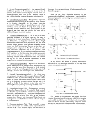
Based on the above discussion regarding all the
parameters described by (1), we formulate a macro-model for
the second generation non-inverting type current conveyor, as
shown in the Fig. 1.
X
0
X2
0
+
-
Gmf
1e-13
0
-
+
+
-
Av r
1e-4
X2
{Ry } Ry
0
{Rz}
Rz
0
0
{Cz}
Cz
Y
0
0
Y
+
-
Gmr
1e-10
{Rx}
Rx
Z
{Lx}
Lx
Z
{Cy }Cy
Air
1e-5
Aif
0.999
0
0
X1
X
Z
0
Y
X2
{Cx}
Cx
0
X1
0
0
-
+
+
-
Av f
0.999
Fig. 1. The Current Conveyor Macromodel
III. CIRCUIT ANALYSIS OF IA TOPOLOGIES
In this section, we present a detailed mathematical
analysis of the two topologies consisting of two and three
current conveyors respectively.
0
R2
{Rload}
CCII+_1
Y
X
Z
a
R1
{Rgain}
OUT
b
CCII+
Y
X
Z
V1
V2
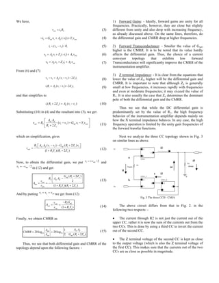
Fig. 2. Two CCII+ Instrumentation Amplifier
Fig. 2 shows the first topology. We analyze the above
circuit to determine its differential gain and CMRR, using the
macro-model described above. Note that such analyses have
been done before, however, while taking simplified models
and only the non-idealities in the voltage and current transfer.
i2i1
We have,
(3)
(4)
(5)
(6)
(7)
From (6) and (7)
(8)
(9)
and that simplifies to
(10)
Substituting (10) in (4) and the resultant into (3), we get
(11)
which on simplification, gives
(12)
Now, to obtain the differential gain, we put 1 / 2dmv v= + and
2 / 2dmv v= − in (12) and get
(13)
And by putting 1 2 cmv v v= = we get from (12)
(14)
Finally, we obtain CMRR as
(15)
Thus, we see that both differential gain and CMRR of the
topology depend upon the following factors: -
1) Forward Gains: - Ideally, forward gains are unity for all
frequencies. Practically, however, they are close but slightly
different from unity and also drop with increasing frequency,
as already discussed above. On the same lines, therefore, do
the differential gain and CMRR drop at higher frequencies.
2) Forward Transconductance: - Smaller the value of Gmf,
higher is the CMRR. It is to be noted that its value hardly
affects the differential gain. Thus, the choice of a current
conveyor topology that exhibits low forward
Transconductance will significantly improve the CMRR of the
instrumentation amplifier.
3) Z terminal Impedance: - It is clear from the equations that
lower the value of Zx, higher will be the differential gain and
CMRR. It is important to note that although Zx is generally
small at low frequencies, it increases rapidly with frequencies
and even at moderate frequencies; it may exceed the value of
R1. It is also usually the case that Zx determines the dominant
pole of both the differential gain and the CMRR.
Thus we see that while the DC differential gain is
predominantly set by the value of R1, the high frequency
behavior of the instrumentation amplifier depends mainly on
how the X terminal impedance behaves. In any case, the high
frequency operation is limited by the unity gain frequencies of
the forward transfer functions.
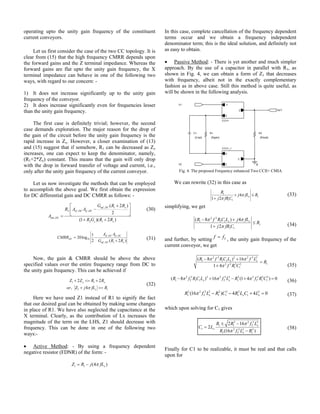
Next we analyze the three CC topology shown in Fig. 3
on similar lines as above.
V1
R1
{Rgain}
R3
{Rload}
V2
OUT
0CCII+_1
Y
X
Z
CCII+_2
Y
X
Z
CCII+
Y
X
Z
Fig. 3 The three CCII+ CMIA
The above circuit differs from that in Fig. 2. in the
following two respects: -
• The current through R2 is not just the current out of the
upper CC, rather it is now the sum of the currents out from the
two CCs. This is done by using a third CC to invert the current
out of the second CC.
• The Z terminal voltage of the second CC is kept as close
to the output voltage (which is also the Z terminal voltage of
the first CC). This makes sure that the currents out of the two
CCs are as close as possible in magnitude.
c i3
i1
2 2outv i R=
2 1 1( )mf if z outi G v A i Y v− = + − +
1 1( ) /a bi v v R= −
1 1( )a if x ir outv A v Z i A v= + − +
2 1b if x ir outv A v Z i A v= + +
1 2 1( ) 2a b if xv v A v v Z i− = − −
1 1 1 2 1( ) 2if xi R A v v Z i= − −
1 1 1 2( 2 ) ( )x ifi R Z A v v+ = −
2 1 2 1
1
( )
2
vf if
out mf z out
x
A A
v R v v G v Y v
R Z
⎡ ⎤
= − − −⎢ ⎥
+⎣ ⎦
2 1 2 1 1
2 1
( ) ( 2 )
(1 )( 2 )
vf if mf x
out
z x
R A A v v G R Z v
v
R Y R Z
⎡ ⎤− − +⎣ ⎦=
+ +
1
2
2 1
( 2 )
2
(1 )( 2 )
mf x
vf if
out
dm
dm z x
G R Z
R A A
v
A
v R Y R Z
+⎡ ⎤
−⎢ ⎥
⎣ ⎦= =
+ +
2
2(1 )
mfout
cm
cm z
R Gv
A
v R Y
−
= =
+
10 10
1
1
20log 20log
2 ( 2 )
vf ifdm
cm mf x
A AA
CMRR
A G R Z
= = −
+
a
b
i2
i4
i5
Let us now proceed to analysis this circuit, in the same fashion
as we did for the previous topology.
We have
(16)
(17)
(18)
neglecting iy,3
(19)
(20)
(21)
(22)
from (20) & (22), we get
(23)
from (16), (17), (18), (19) & (23), we get
(24)
simplifying
(25)
(26)
Now, to obtain the differential gain, we put 1 / 2dmv v= +
and
2 / 2dmv v= − in (26) and get
(27)
and by putting 1 2 cmv v v= =
we get from (26)
(28)
Finally, we obtain CMRR as
(29)
Let us now compare (15) and (29). The CMRR in both
cases depends upon the forward current gains and inversely on
the value of R1. Whereas in case of two CC topology, the
effect of Zx is to reduce the CMRR as it increases with
frequency, its effect in case of three CC topology is much
more pronounced. In the latter case, it combines with Yz to
produce the following two effects: -
1) For low frequencies, their effect is to provide a large
increase in CMRR as compared to that in two CC topology.
For example, with Zx = 10 ohm & Yz = 10-7
mho, an increase
of 66 dB in CMRR is observed, as is verified in the simulation
results as well.
Let us now try to understand qualitatively such a
phenomenal increase in CMRR. In the differential mode, the
third CC reverses the direction of i3 and the result is that the
current through R2 is now double the magnitude as compared
to that in two CC case. This effectively doubles the
differential gain, which explains one of the fractions of
observed increase.
The most important contribution to the increase, however,
is in the common mode operation. In this mode, the current i1
is virtually zero, which essentially leaves away only the offset
components in currents i2 and i3. These currents are in the
same direction and the third CC inverts one of them, to the
result that now the current through R2 is the difference of i2
and i3. This current is very much smaller than what flows
through in the case of two CC topology, and this explains the
highly reduced common mode gain in the three CC topology.
The combined effect is the large increase in CMRR, as
observed.
2) Whereas Zx introduces a first order pole in the CMRR of
the two CC topology, the combined effect of Zx and Yz is
responsible for a second order pole in the CMRR of the three
CC topology. This effect also creates a problem, as we will
discuss in the section on bandwidth optimization.
IV. BANDWIDTH OPTIMIZATION TECHNIQUES
One of the main advantages of current mode circuits is
their inherent gain independent bandwidth. This is also the
expected case with the above circuits. However as we see
below, there are parasitic effects that restrict the circuits from
5 2outv i R=
5 2 4i i i= +
2 1 1( )mf if z outi G v A i Y v− = + − +
4 ,3 3( ( ) )z mf out if z outi i G v A i Y v= = − + − +
3 2 1mf if z ci G v A i Y v= + +
1 1 2 1( ) /i v v R= −
3( )c vf out x vr outv A v Z i A v= + − +
3 2 1(1 ) ( )z x mf if z vf vr outi Y Z G v A i Y A A v+ = + + +
2 1
2 1 1
( )
[ ( 2 ) ( )]
(1 )
mf if z vf vr out
out mf mf z out if
z x
G v A i Y A A v
v R G v G Y v A i
Y Z
+ + +
− = + + − +
+
2 1
1 2
[ (1 ) ( 2 )(1 )
{(1 ) ( ) }]
out mf z x mf z z x out
if z x if mf z vf vr out
v R G Y Z v G Y Y Z v
A Y Z A i G v Y A A v
− = + + + +
− + + + + +
1 2
2 1 1 2 1 2 2 1 2
[ {( 2 )(1 ) ( )} 1]
(1 ) (1 )( )
mf z z x z if vf vr out
mf z x mf if if z x if
R R G Y Y Z Y A A A v
R R G Y Z v R R G A v R A Y Z A v v
− + + − + +
= + − − + + −
12
1 2
(1 )
2 [ {( 2 )(1 ) ( )} 1]
mf z x ifout
dm if
dm mf z z x z if vf vr
R G Y Z Av R
A A
v R R G Y Y Z Y A A A
+ +⎛ ⎞
= = −⎜ ⎟
+ + − + +⎝ ⎠
2
2
(1 )
[ {( 2 )(1 ) ( )} 1]
mf z x ifout
cm
cm mf z z x z if vf vr
R G Y Z Av
A
v R G Y Y Z Y A A A
− + −
= =
+ + − + +
10 10
1
11
20log 20log
2 1
if z x ifdm
cm mf z x if
A Y Z AA
CMRR
A R G Y Z A
⎛ ⎞⎛ ⎞+ +
= = −⎜ ⎟⎜ ⎟⎜ ⎟⎜ ⎟+ −⎝ ⎠⎝ ⎠
operating upto the unity gain frequency of the constituent
current conveyors.
Let us first consider the case of the two CC topology. It is
clear from (15) that the high frequency CMRR depends upon
the forward gains and the Z terminal impedance. Whereas the
forward gains are flat upto the unity gain frequency, the X
terminal impedance can behave in one of the following two
ways, with regard to our concern: -
1) It does not increase significantly up to the unity gain
frequency of the conveyor.
2) It does increase significantly even for frequencies lesser
than the unity gain frequency.
The first case is definitely trivial; however, the second
case demands exploration. The major reason for the drop of
the gain of the circuit before the unity gain frequency is the
rapid increase in Zx. However, a closer examination of (13)
and (15) suggest that if somehow, R1 can be decreased as Zx
increases, one can expect to keep the denominator, namely,
(R1+2*Zx) constant. This means that the gain will only drop
with the drop in forward transfer of voltage and current, i.e.,
only after the unity gain frequency of the current conveyor.
Let us now investigate the methods that can be employed
to accomplish the above goal. We first obtain the expression
for DC differential gain and DC CMRR as follows: -
(30)
(31)
Now, the gain & CMRR should be above the above
specified values over the entire frequency range from DC to
the unity gain frequency. This can be achieved if
(32)
Here we have used Z1 instead of R1 to signify the fact
that our desired goal can be obtained by making some changes
in place of R1. We have also neglected the capacitance at the
X terminal. Clearly, as the contribution of Lx increases the
magnitude of the term on the LHS, Z1 should decrease with
frequency. This can be done in one of the following two
ways:-
• Active Method: - By using a frequency dependent
negative resistor (FDNR) of the form: -
1 1 (4 )xZ R j fLπ= −
In this case, complete cancellation of the frequency dependent
terms occur and we obtain a frequency independent
denominator term; this is the ideal solution, and definitely not
as easy to obtain.
• Passive Method: - There is yet another and much simpler
approach. By the use of a capacitor in parallel with R1, as
shown in Fig. 4, we can obtain a form of Z1 that decreases
with frequency, albeit not in the exactly complementary
fashion as in above case. Still this method is quite useful, as
will be shown in the following analysis.
V2
CCII+
Y
X
Z
V1
OUT
R2
{Rload}
CCII+_1
Y
X
Z
R1
{Rgain}
C1
{Copt}
0
Fig. 4. The proposed Frequency enhanced Two CCII+ CMIA
We can rewrite (32) in this case as
(33)
simplifying, we get
(34)
and further, by setting Tf f= , the unity gain frequency of the
current conveyor, we get
(35)
(36)
(37)
which upon solving for C1 gives
(38)
Finally for C1 to be realizable, it must be real and that calls
upon for
, ,
10
, 1
1
20log
2 ( 2 )
vf DC if DC
DC
mf DC x
A A
CMRR
G R R
= −
+
, 1
2 , ,
,
2 1
( 2 )
2
(1 )( 2 )
mf DC x
vf DC if DC
dm DC
z x
G R R
R A A
A
R G R R
+⎡ ⎤
−⎢ ⎥
⎣ ⎦=
+ +
1 1
1 1
2 2
, Z 4
x x
x
Z Z R R
or j fL Rπ
+ <= +
+ <=
1
1
1 1
4
1 2
x
R
j fL R
j fRC
π
π
+ ≤
+
2 2
1 1 1
1
1 1
( 8 ) 4
1 2
x xR f R C L j fL
R
j fR C
π π
π
− +
≤
+
2 2 2 2 2 2
1 1 1
12 2 2 2
1 1
( 8 ) 16
1 4
x xR f R C L f L
R
f R C
π π
π
− +
=
+
2 2 2 2 2 2 2 2 2 2 2
1 1 1 1 1 1( 8 ) 16 (1 4 ) 0T x T x TR f R C L f L R f R Cπ π π− + − + =
2 2 2 2 2 2 2 2
1 1 1 1 1(16 ) 4 4 0T x x xR f L R C R L C Lπ − − + =
2 2 2 2
1 1
1 2 2 2 2
1 1
2 16
2
(16 )
T x
x
T x
R R f L
C L
R f L R
π
π
± −
=
−
(39)
Let us try to interpret (38). In one sense, it says that the
proposed scheme works only up to a limited frequency. There
is no value of C1 that can enhance the bandwidth above a
certain limit, which is given by (38). However, this is only
half the story. By increasing the value of R1, this limit can also
be increased. But increasing R1 would decrease the gain /
CMRR and in this regard, the circuit does not exhibit
bandwidth independent gain / CMRR.
Now in a manner similar to that of the 2 CCII+ circuit, for
the three CC circuit we can optimize the high frequency
behaviour using a capacitor in parallel with R1. This can be
explained as following.
As frequency increases, the product YzZx increases. This
means that the denominator in the CMRR expression increases
with frequency and thus the CMRR decreases. Now the only
term that can be exploited to overcome this decrease in CMRR
is R1. If we decrease the effective value of R1 by some means
with frequency, we can obtain a nearly constant CMRR over a
wider frequency range, i.e. upto the unity gain frequency of
the current conveyor. On the similar lines as above, therefore
we add a capacitor in parallel with R1 to achieve the effect.
The analysis of the same follows below.
To keep CMRR constant, we need 1
11
1
z x if
z x if
Y Z A
Z Y Z A
⎛ ⎞+ +
⎜ ⎟⎜ ⎟+ −⎝ ⎠ to be
constant over the desired frequency range. This can be written
as
(40)
Under the approximation that
1 z x ifY Z A+ +
remains relatively
constant over the frequencies of interest, and approximately
equal to 2, we get
(41)
Let us call 1 z x ifoG R A K+ − =
, and thus
(42)
The above equation clearly shows that this scheme
would not work in this case, at least the passive solution. The
denominator has a second order increase while a passive Z1
can at most decrease in a first order fashion. It may be
possible to obtain the desired results using an active scheme,
such as using a D-type FDNR in place of C1. This technique
can be further explored to obtain superior performance.
V. SIMULATION & RESULTS
In this section we present the results obtained from
PSPICE simulations. We have used the current conveyor
implementation as presented in [4]. Table 1 shows the various
parameters used in (1) for the CC implementation. The values
of R1 and R2 are taken to be 100 ohm each. The results are in
close agreement with the theoretical analysis presented above.
TABLE I
CC IMPLEMENTATION PARAMETERS
Parameter Value
Gy 10-16
mho
Cy I59 Ff
Rx 0.3 ohm
Lx 27 uH
Gz 31 nano-ohm
Cz 10 fF
Aif 1; -3dB = 20 MHz
Avf 1; -3dB = 20 MHz
Gmf 31 nano-mho; -3 dB = 100 kHz
Fig. 5 shows the CMRR vs Frequency for the two CC
topology. The theoretical DC CMRR in this case comes out to
be 109.6 dB, very close to the simulated 109.1 dB.
Fig. 5. Two CCII+ instrumentation amplifier CMRR vs. Frequency
Curve
Fig. 6. Two CCII+ instrumentation amplifier CMRR vs. Frequency
Curve with bandwidth optimization.
Fig. 6 shows the CMRR plot with C in place. The values
of C are taken to be 1nF, 33nF & 100nF. The first value of C
is too small to cause any appreciable effect. The last value of
100 nF turns to be too large for the purpose and this is shown
by a peak. The second value of 33nF seems to be close to the
1
2 2
T
x
R
f
Lπ
≤
1 1
1 11 1
1 1
z x if z x ifo
z x if z x ifo
Y Z A G R A
Z Y Z A R G R A
⎛ ⎞ ⎛ ⎞+ + + +
≥⎜ ⎟ ⎜ ⎟⎜ ⎟ ⎜ ⎟+ − + −⎝ ⎠ ⎝ ⎠
1 1
1 1
1 2 2 1 2
1 1z x if z x ifo
j R C
R Y Z A R G R A
π ⎛ ⎞ ⎛ ⎞+
≥⎜ ⎟ ⎜ ⎟⎜ ⎟ ⎜ ⎟+ − + −⎝ ⎠ ⎝ ⎠
1 11 2 1
1 ( 2 )( 2 )z z x x if
j fR C
G j fC R j fL A K
π
π π
+
≥
+ + + −
requirement, which is able to push the bandwidth to 141.1 kHz
without any appreciable overshoot.
Fig. 7. Three CCII+ instrumentation amplifier CMRR vs. Frequency
Curve.
Fig. 7 shows the CMRR vs Frequency curve for three CC
topology. The theoretical DC CMRR comes out to be 276.8
dB, which is close to 268.8 dB, as obtained from the
simulation.
VI. CONCLUSIONS
In this paper we have studied two IA topologies and
presented a comprehensive mathematical analysis based on a
linear CC model. The theoretical results have been verified
with the help of PSPICE simulations. An explanation has been
provided for the observed increase in the CMRR of the three
CC topology. Also, results have been provided showing the
bandwidth enhancement of the two CC topology. Further
another method has been suggested for bandwidth
improvement of the three CC topology.
VII. REFERENCES
[1] Toumozou, Lidgey & Haigh, “Analog IC Design – The Current Mode
Approach”
[2] C. Toumazou and F. Lidgey, “Novel current-mode instrumentation
amplifier,” Electron. Lett., vol. 25, pp. 228–230, Feb. 1989.
[3] Anwar A. Khan,Mohammed A. Al-Turaigi, Mohamed Abou El-Ela,
“An Improved Current-Mode Instrumentation Amplifier with
Bandwidth independent of Gain”, IEEE Transactions on Instrumentation
and Measurement, Vol. 44. No. 4, August 1995
[4] Hassan O. Elwan and Ahmed M. Soliman, “Low-Voltage Low-Power
CMOS Current Conveyors.” IEEE TRANSACTIONS ON CIRCUITS
AND SYSTEMS—I: FUNDAMENTAL THEORY AND APPLICATIONS,
VOL. 44, NO. 9, SEPTEMBER 1997
VII. ABOUT THE AUTHORS
The authors are final year undergraduate students at the
Department of Electronics & Communication Engineering at
Delhi College of Engineering, Delhi, India. Their interests lie
in the fields of CMOS analog circuit design & embedded
systems, especially in the field of communication & signal
processing systems. They plan to further their interests in
these fields by working in industry and going for higher
studies in the same.
CMIA paper

CMIA paper

  • 1.
    An Analysis ofCurrent Mode Instrumentation Amplifier Topologies & Methods of Bandwidth Improvement Sunny Gupta, Nitin Gandhi, Kunal Gupta, Hemant Mudgal Department of Electronics Engineering Delhi College of Engineering Bawana Road, Delhi, India 110042 Abstract- In this paper we present the analysis of two current-mode instrumentation amplifier topologies and highlight upon some of the subtle yet important characteristics of the same. Based on a comprehensive mathematical analysis, we suggest methods to improve the circuit bandwidth upto the unity gain frequency of the constituent current conveyors. Further our analysis also justifies the highly improved CMRR observed in one of the IA topology. I. INTRODUCTION High performance instrumentation amplifiers are in demand in all kinds of applications where common mode signal suppression is desired. Conventional designs of instrumentation amplifier are based on voltage feedback operational amplifiers. These designs rely on precise matching between resistors to obtain high CMRR. Moreover, due to finite gain-bandwidth product of VOAs, these designs are limited to very low frequencies of operation with high gain. Recently, the inherent advantages of current mode analog circuits [1] have reflected into instrumentation amplifier designs as well, and many topologies have been proposed based on the initial proposal [2]. An improved performance was shown to have been obtained in the topology presented in [3]. However the analysis presented in the previous works have used simplified models of current conveyors. These only consider the non-idealities in current and voltage transfer and ignore some of the important parameters such as X and Z terminal impedances and parasitic transfer terms. In this paper we use a standard non-ideal model of a current conveyor, which is explained in the next section, to analyze the two standard topologies. This leads us to a variety of interesting results that help us propose techniques to improve the bandwidth of the circuit and moreover justify the observed improvement in the CMRR. II. THE CURRENT CONVEYOR MODEL A general representation of a current conveyor is given by (1), (1) which, for the ideal case becomes, (2) with the values of the triplet (a,b,c) deciding the generation and type of current conveyor. Let us now explain each of the current conveyor parameters in (1), with reference to a second generation non- inverting type current conveyor (CCII+) 1) Y terminal admittance (Yy): - Ideally, it should be zero, as no Y terminal current is allowed, irrespective of the Y terminal voltage and operating frequency. However, as in most of the cases, Y terminal of a current conveyor is directly connected to the gate of a MOSFET; this parameter depends on frequency, dominantly due to the MOSFET gate capacitance. In most of the cases, therefore, Yy can be represented by a first order RC admittance, as a close and valid approximation. 2) Reverse Current Gain (Air): - The dependence of Y terminal current on the X terminal current is depicted in this parameter, which is ideally zero. However, as X terminal of a CMOS current conveyor is usually a source follower, channel length modulation plays its role to affect the Y terminal input stage voltages, which in turn affect the Y terminal voltage dependent capacitances. Overall, this parameter is quite small over the lower range of frequencies, and it grows exponentially with increasing frequencies; this is due to the fact that channel length modulation effect becomes more significant at higher frequencies. ⎥ ⎥ ⎥ ⎦ ⎤ ⎢ ⎢ ⎢ ⎣ ⎡ ⎥ ⎥ ⎥ ⎦ ⎤ ⎢ ⎢ ⎢ ⎣ ⎡ = ⎥ ⎥ ⎥ ⎦ ⎤ ⎢ ⎢ ⎢ ⎣ ⎡ z x y zifmf vrxvf mriry z x y v i v YAG AZA GAY i v i 0 0 0 0 0 0 y y x x z z i a v v b i i c v ⎡ ⎤ ⎡ ⎤ ⎡ ⎤ ⎢ ⎥ ⎢ ⎥ ⎢ ⎥=⎢ ⎥ ⎢ ⎥ ⎢ ⎥ ⎢ ⎥ ⎢ ⎥ ⎢ ⎥⎣ ⎦ ⎣ ⎦ ⎣ ⎦
  • 2.
    3) Reverse Transconductance(Gmr): - Just as channel length modulation operates as X terminal, so it does at the Z terminal, albeit to a much smaller degree; however, it still has, thought negligibly small effect on the Y terminal current. It also exhibits a similar frequency dependent behavior as Air. 4) Forward voltage gain (Avf): - This parameter represents the transfer of voltage from the Y terminal to the X terminal, as is therefore responsible for the voltage conveying operation. It exhibits a behavior typical of a unity gain voltage amplifier, whose gain begins to drop from unity as the frequency increases above the unity gain frequency of the devices in use. Here again, the use of a first order pole is sufficient for quite an accurate analysis. 5) X terminal Impedance (Zx): - This is one of the most important parameter of a current conveyor. The more it deviates from its ideal value of zero, the performance of the CC deteriorates. As frequency increases, channel length modulation effect becomes more predominant, and thus the X terminal voltage becomes more and more dependent on the current into the X terminal, and thus we see that there is a strong inductive component in Zx. However, there is still a small capacitive component due to the parasitic MOS capacitances. Overall, such a combination makes second order RLC impedance at the X terminal that might occasionally have resonant minimum impedance at an intermediate frequency. However, such an observation is not very common due to the fact that X terminal capacitance is quite insignificant as compared to its impedance. 6) Reverse voltage gain (Avr): - Again due to the channel length modulation in the current mirror configuration for current conveying action from X terminal to the Z terminal, there is a small reverse voltage gain that is usually very small, although it increases with frequency in a first order manner. 7) Forward Transconductance (Gmf): - The culprit keeps emerging again and again, and here’s again the channel length modulation at the X terminal that helps X terminal voltage control the current at Z terminal, though slightly. This is again one of the important parameters, as we shall see later, with regard to CMIA. It also exhibits a first order zero type frequency behaviour, although has a very small DC value. 8) Forward current gain (Aif): - This parameter represents the transfer of current from the X terminal to the Z terminal, as is therefore responsible for the current conveying operation. It exhibits a behavior typical of a unity gain current amplifier, whose gain begins to drop from unity as the frequency increases above the unity gain frequency of the devices in use. Here again, the use of a first order pole is sufficient for quite an accurate analysis. 9) Z terminal admittance (Yz): - The Z terminal is a typical current mirror output, and exhibits similar output admittance; very low at DC, which increases rapidly with the increase in frequency. However, a single order RC admittance suffices for the analysis purpose. Based on the above discussion regarding all the parameters described by (1), we formulate a macro-model for the second generation non-inverting type current conveyor, as shown in the Fig. 1. X 0 X2 0 + - Gmf 1e-13 0 - + + - Av r 1e-4 X2 {Ry } Ry 0 {Rz} Rz 0 0 {Cz} Cz Y 0 0 Y + - Gmr 1e-10 {Rx} Rx Z {Lx} Lx Z {Cy }Cy Air 1e-5 Aif 0.999 0 0 X1 X Z 0 Y X2 {Cx} Cx 0 X1 0 0 - + + - Av f 0.999 Fig. 1. The Current Conveyor Macromodel III. CIRCUIT ANALYSIS OF IA TOPOLOGIES In this section, we present a detailed mathematical analysis of the two topologies consisting of two and three current conveyors respectively. 0 R2 {Rload} CCII+_1 Y X Z a R1 {Rgain} OUT b CCII+ Y X Z V1 V2 Fig. 2. Two CCII+ Instrumentation Amplifier Fig. 2 shows the first topology. We analyze the above circuit to determine its differential gain and CMRR, using the macro-model described above. Note that such analyses have been done before, however, while taking simplified models and only the non-idealities in the voltage and current transfer. i2i1
  • 3.
    We have, (3) (4) (5) (6) (7) From (6)and (7) (8) (9) and that simplifies to (10) Substituting (10) in (4) and the resultant into (3), we get (11) which on simplification, gives (12) Now, to obtain the differential gain, we put 1 / 2dmv v= + and 2 / 2dmv v= − in (12) and get (13) And by putting 1 2 cmv v v= = we get from (12) (14) Finally, we obtain CMRR as (15) Thus, we see that both differential gain and CMRR of the topology depend upon the following factors: - 1) Forward Gains: - Ideally, forward gains are unity for all frequencies. Practically, however, they are close but slightly different from unity and also drop with increasing frequency, as already discussed above. On the same lines, therefore, do the differential gain and CMRR drop at higher frequencies. 2) Forward Transconductance: - Smaller the value of Gmf, higher is the CMRR. It is to be noted that its value hardly affects the differential gain. Thus, the choice of a current conveyor topology that exhibits low forward Transconductance will significantly improve the CMRR of the instrumentation amplifier. 3) Z terminal Impedance: - It is clear from the equations that lower the value of Zx, higher will be the differential gain and CMRR. It is important to note that although Zx is generally small at low frequencies, it increases rapidly with frequencies and even at moderate frequencies; it may exceed the value of R1. It is also usually the case that Zx determines the dominant pole of both the differential gain and the CMRR. Thus we see that while the DC differential gain is predominantly set by the value of R1, the high frequency behavior of the instrumentation amplifier depends mainly on how the X terminal impedance behaves. In any case, the high frequency operation is limited by the unity gain frequencies of the forward transfer functions. Next we analyze the three CC topology shown in Fig. 3 on similar lines as above. V1 R1 {Rgain} R3 {Rload} V2 OUT 0CCII+_1 Y X Z CCII+_2 Y X Z CCII+ Y X Z Fig. 3 The three CCII+ CMIA The above circuit differs from that in Fig. 2. in the following two respects: - • The current through R2 is not just the current out of the upper CC, rather it is now the sum of the currents out from the two CCs. This is done by using a third CC to invert the current out of the second CC. • The Z terminal voltage of the second CC is kept as close to the output voltage (which is also the Z terminal voltage of the first CC). This makes sure that the currents out of the two CCs are as close as possible in magnitude. c i3 i1 2 2outv i R= 2 1 1( )mf if z outi G v A i Y v− = + − + 1 1( ) /a bi v v R= − 1 1( )a if x ir outv A v Z i A v= + − + 2 1b if x ir outv A v Z i A v= + + 1 2 1( ) 2a b if xv v A v v Z i− = − − 1 1 1 2 1( ) 2if xi R A v v Z i= − − 1 1 1 2( 2 ) ( )x ifi R Z A v v+ = − 2 1 2 1 1 ( ) 2 vf if out mf z out x A A v R v v G v Y v R Z ⎡ ⎤ = − − −⎢ ⎥ +⎣ ⎦ 2 1 2 1 1 2 1 ( ) ( 2 ) (1 )( 2 ) vf if mf x out z x R A A v v G R Z v v R Y R Z ⎡ ⎤− − +⎣ ⎦= + + 1 2 2 1 ( 2 ) 2 (1 )( 2 ) mf x vf if out dm dm z x G R Z R A A v A v R Y R Z +⎡ ⎤ −⎢ ⎥ ⎣ ⎦= = + + 2 2(1 ) mfout cm cm z R Gv A v R Y − = = + 10 10 1 1 20log 20log 2 ( 2 ) vf ifdm cm mf x A AA CMRR A G R Z = = − + a b i2 i4 i5
  • 4.
    Let us nowproceed to analysis this circuit, in the same fashion as we did for the previous topology. We have (16) (17) (18) neglecting iy,3 (19) (20) (21) (22) from (20) & (22), we get (23) from (16), (17), (18), (19) & (23), we get (24) simplifying (25) (26) Now, to obtain the differential gain, we put 1 / 2dmv v= + and 2 / 2dmv v= − in (26) and get (27) and by putting 1 2 cmv v v= = we get from (26) (28) Finally, we obtain CMRR as (29) Let us now compare (15) and (29). The CMRR in both cases depends upon the forward current gains and inversely on the value of R1. Whereas in case of two CC topology, the effect of Zx is to reduce the CMRR as it increases with frequency, its effect in case of three CC topology is much more pronounced. In the latter case, it combines with Yz to produce the following two effects: - 1) For low frequencies, their effect is to provide a large increase in CMRR as compared to that in two CC topology. For example, with Zx = 10 ohm & Yz = 10-7 mho, an increase of 66 dB in CMRR is observed, as is verified in the simulation results as well. Let us now try to understand qualitatively such a phenomenal increase in CMRR. In the differential mode, the third CC reverses the direction of i3 and the result is that the current through R2 is now double the magnitude as compared to that in two CC case. This effectively doubles the differential gain, which explains one of the fractions of observed increase. The most important contribution to the increase, however, is in the common mode operation. In this mode, the current i1 is virtually zero, which essentially leaves away only the offset components in currents i2 and i3. These currents are in the same direction and the third CC inverts one of them, to the result that now the current through R2 is the difference of i2 and i3. This current is very much smaller than what flows through in the case of two CC topology, and this explains the highly reduced common mode gain in the three CC topology. The combined effect is the large increase in CMRR, as observed. 2) Whereas Zx introduces a first order pole in the CMRR of the two CC topology, the combined effect of Zx and Yz is responsible for a second order pole in the CMRR of the three CC topology. This effect also creates a problem, as we will discuss in the section on bandwidth optimization. IV. BANDWIDTH OPTIMIZATION TECHNIQUES One of the main advantages of current mode circuits is their inherent gain independent bandwidth. This is also the expected case with the above circuits. However as we see below, there are parasitic effects that restrict the circuits from 5 2outv i R= 5 2 4i i i= + 2 1 1( )mf if z outi G v A i Y v− = + − + 4 ,3 3( ( ) )z mf out if z outi i G v A i Y v= = − + − + 3 2 1mf if z ci G v A i Y v= + + 1 1 2 1( ) /i v v R= − 3( )c vf out x vr outv A v Z i A v= + − + 3 2 1(1 ) ( )z x mf if z vf vr outi Y Z G v A i Y A A v+ = + + + 2 1 2 1 1 ( ) [ ( 2 ) ( )] (1 ) mf if z vf vr out out mf mf z out if z x G v A i Y A A v v R G v G Y v A i Y Z + + + − = + + − + + 2 1 1 2 [ (1 ) ( 2 )(1 ) {(1 ) ( ) }] out mf z x mf z z x out if z x if mf z vf vr out v R G Y Z v G Y Y Z v A Y Z A i G v Y A A v − = + + + + − + + + + + 1 2 2 1 1 2 1 2 2 1 2 [ {( 2 )(1 ) ( )} 1] (1 ) (1 )( ) mf z z x z if vf vr out mf z x mf if if z x if R R G Y Y Z Y A A A v R R G Y Z v R R G A v R A Y Z A v v − + + − + + = + − − + + − 12 1 2 (1 ) 2 [ {( 2 )(1 ) ( )} 1] mf z x ifout dm if dm mf z z x z if vf vr R G Y Z Av R A A v R R G Y Y Z Y A A A + +⎛ ⎞ = = −⎜ ⎟ + + − + +⎝ ⎠ 2 2 (1 ) [ {( 2 )(1 ) ( )} 1] mf z x ifout cm cm mf z z x z if vf vr R G Y Z Av A v R G Y Y Z Y A A A − + − = = + + − + + 10 10 1 11 20log 20log 2 1 if z x ifdm cm mf z x if A Y Z AA CMRR A R G Y Z A ⎛ ⎞⎛ ⎞+ + = = −⎜ ⎟⎜ ⎟⎜ ⎟⎜ ⎟+ −⎝ ⎠⎝ ⎠
  • 5.
    operating upto theunity gain frequency of the constituent current conveyors. Let us first consider the case of the two CC topology. It is clear from (15) that the high frequency CMRR depends upon the forward gains and the Z terminal impedance. Whereas the forward gains are flat upto the unity gain frequency, the X terminal impedance can behave in one of the following two ways, with regard to our concern: - 1) It does not increase significantly up to the unity gain frequency of the conveyor. 2) It does increase significantly even for frequencies lesser than the unity gain frequency. The first case is definitely trivial; however, the second case demands exploration. The major reason for the drop of the gain of the circuit before the unity gain frequency is the rapid increase in Zx. However, a closer examination of (13) and (15) suggest that if somehow, R1 can be decreased as Zx increases, one can expect to keep the denominator, namely, (R1+2*Zx) constant. This means that the gain will only drop with the drop in forward transfer of voltage and current, i.e., only after the unity gain frequency of the current conveyor. Let us now investigate the methods that can be employed to accomplish the above goal. We first obtain the expression for DC differential gain and DC CMRR as follows: - (30) (31) Now, the gain & CMRR should be above the above specified values over the entire frequency range from DC to the unity gain frequency. This can be achieved if (32) Here we have used Z1 instead of R1 to signify the fact that our desired goal can be obtained by making some changes in place of R1. We have also neglected the capacitance at the X terminal. Clearly, as the contribution of Lx increases the magnitude of the term on the LHS, Z1 should decrease with frequency. This can be done in one of the following two ways:- • Active Method: - By using a frequency dependent negative resistor (FDNR) of the form: - 1 1 (4 )xZ R j fLπ= − In this case, complete cancellation of the frequency dependent terms occur and we obtain a frequency independent denominator term; this is the ideal solution, and definitely not as easy to obtain. • Passive Method: - There is yet another and much simpler approach. By the use of a capacitor in parallel with R1, as shown in Fig. 4, we can obtain a form of Z1 that decreases with frequency, albeit not in the exactly complementary fashion as in above case. Still this method is quite useful, as will be shown in the following analysis. V2 CCII+ Y X Z V1 OUT R2 {Rload} CCII+_1 Y X Z R1 {Rgain} C1 {Copt} 0 Fig. 4. The proposed Frequency enhanced Two CCII+ CMIA We can rewrite (32) in this case as (33) simplifying, we get (34) and further, by setting Tf f= , the unity gain frequency of the current conveyor, we get (35) (36) (37) which upon solving for C1 gives (38) Finally for C1 to be realizable, it must be real and that calls upon for , , 10 , 1 1 20log 2 ( 2 ) vf DC if DC DC mf DC x A A CMRR G R R = − + , 1 2 , , , 2 1 ( 2 ) 2 (1 )( 2 ) mf DC x vf DC if DC dm DC z x G R R R A A A R G R R +⎡ ⎤ −⎢ ⎥ ⎣ ⎦= + + 1 1 1 1 2 2 , Z 4 x x x Z Z R R or j fL Rπ + <= + + <= 1 1 1 1 4 1 2 x R j fL R j fRC π π + ≤ + 2 2 1 1 1 1 1 1 ( 8 ) 4 1 2 x xR f R C L j fL R j fR C π π π − + ≤ + 2 2 2 2 2 2 1 1 1 12 2 2 2 1 1 ( 8 ) 16 1 4 x xR f R C L f L R f R C π π π − + = + 2 2 2 2 2 2 2 2 2 2 2 1 1 1 1 1 1( 8 ) 16 (1 4 ) 0T x T x TR f R C L f L R f R Cπ π π− + − + = 2 2 2 2 2 2 2 2 1 1 1 1 1(16 ) 4 4 0T x x xR f L R C R L C Lπ − − + = 2 2 2 2 1 1 1 2 2 2 2 1 1 2 16 2 (16 ) T x x T x R R f L C L R f L R π π ± − = −
  • 6.
    (39) Let us tryto interpret (38). In one sense, it says that the proposed scheme works only up to a limited frequency. There is no value of C1 that can enhance the bandwidth above a certain limit, which is given by (38). However, this is only half the story. By increasing the value of R1, this limit can also be increased. But increasing R1 would decrease the gain / CMRR and in this regard, the circuit does not exhibit bandwidth independent gain / CMRR. Now in a manner similar to that of the 2 CCII+ circuit, for the three CC circuit we can optimize the high frequency behaviour using a capacitor in parallel with R1. This can be explained as following. As frequency increases, the product YzZx increases. This means that the denominator in the CMRR expression increases with frequency and thus the CMRR decreases. Now the only term that can be exploited to overcome this decrease in CMRR is R1. If we decrease the effective value of R1 by some means with frequency, we can obtain a nearly constant CMRR over a wider frequency range, i.e. upto the unity gain frequency of the current conveyor. On the similar lines as above, therefore we add a capacitor in parallel with R1 to achieve the effect. The analysis of the same follows below. To keep CMRR constant, we need 1 11 1 z x if z x if Y Z A Z Y Z A ⎛ ⎞+ + ⎜ ⎟⎜ ⎟+ −⎝ ⎠ to be constant over the desired frequency range. This can be written as (40) Under the approximation that 1 z x ifY Z A+ + remains relatively constant over the frequencies of interest, and approximately equal to 2, we get (41) Let us call 1 z x ifoG R A K+ − = , and thus (42) The above equation clearly shows that this scheme would not work in this case, at least the passive solution. The denominator has a second order increase while a passive Z1 can at most decrease in a first order fashion. It may be possible to obtain the desired results using an active scheme, such as using a D-type FDNR in place of C1. This technique can be further explored to obtain superior performance. V. SIMULATION & RESULTS In this section we present the results obtained from PSPICE simulations. We have used the current conveyor implementation as presented in [4]. Table 1 shows the various parameters used in (1) for the CC implementation. The values of R1 and R2 are taken to be 100 ohm each. The results are in close agreement with the theoretical analysis presented above. TABLE I CC IMPLEMENTATION PARAMETERS Parameter Value Gy 10-16 mho Cy I59 Ff Rx 0.3 ohm Lx 27 uH Gz 31 nano-ohm Cz 10 fF Aif 1; -3dB = 20 MHz Avf 1; -3dB = 20 MHz Gmf 31 nano-mho; -3 dB = 100 kHz Fig. 5 shows the CMRR vs Frequency for the two CC topology. The theoretical DC CMRR in this case comes out to be 109.6 dB, very close to the simulated 109.1 dB. Fig. 5. Two CCII+ instrumentation amplifier CMRR vs. Frequency Curve Fig. 6. Two CCII+ instrumentation amplifier CMRR vs. Frequency Curve with bandwidth optimization. Fig. 6 shows the CMRR plot with C in place. The values of C are taken to be 1nF, 33nF & 100nF. The first value of C is too small to cause any appreciable effect. The last value of 100 nF turns to be too large for the purpose and this is shown by a peak. The second value of 33nF seems to be close to the 1 2 2 T x R f Lπ ≤ 1 1 1 11 1 1 1 z x if z x ifo z x if z x ifo Y Z A G R A Z Y Z A R G R A ⎛ ⎞ ⎛ ⎞+ + + + ≥⎜ ⎟ ⎜ ⎟⎜ ⎟ ⎜ ⎟+ − + −⎝ ⎠ ⎝ ⎠ 1 1 1 1 1 2 2 1 2 1 1z x if z x ifo j R C R Y Z A R G R A π ⎛ ⎞ ⎛ ⎞+ ≥⎜ ⎟ ⎜ ⎟⎜ ⎟ ⎜ ⎟+ − + −⎝ ⎠ ⎝ ⎠ 1 11 2 1 1 ( 2 )( 2 )z z x x if j fR C G j fC R j fL A K π π π + ≥ + + + −
  • 7.
    requirement, which isable to push the bandwidth to 141.1 kHz without any appreciable overshoot. Fig. 7. Three CCII+ instrumentation amplifier CMRR vs. Frequency Curve. Fig. 7 shows the CMRR vs Frequency curve for three CC topology. The theoretical DC CMRR comes out to be 276.8 dB, which is close to 268.8 dB, as obtained from the simulation. VI. CONCLUSIONS In this paper we have studied two IA topologies and presented a comprehensive mathematical analysis based on a linear CC model. The theoretical results have been verified with the help of PSPICE simulations. An explanation has been provided for the observed increase in the CMRR of the three CC topology. Also, results have been provided showing the bandwidth enhancement of the two CC topology. Further another method has been suggested for bandwidth improvement of the three CC topology. VII. REFERENCES [1] Toumozou, Lidgey & Haigh, “Analog IC Design – The Current Mode Approach” [2] C. Toumazou and F. Lidgey, “Novel current-mode instrumentation amplifier,” Electron. Lett., vol. 25, pp. 228–230, Feb. 1989. [3] Anwar A. Khan,Mohammed A. Al-Turaigi, Mohamed Abou El-Ela, “An Improved Current-Mode Instrumentation Amplifier with Bandwidth independent of Gain”, IEEE Transactions on Instrumentation and Measurement, Vol. 44. No. 4, August 1995 [4] Hassan O. Elwan and Ahmed M. Soliman, “Low-Voltage Low-Power CMOS Current Conveyors.” IEEE TRANSACTIONS ON CIRCUITS AND SYSTEMS—I: FUNDAMENTAL THEORY AND APPLICATIONS, VOL. 44, NO. 9, SEPTEMBER 1997 VII. ABOUT THE AUTHORS The authors are final year undergraduate students at the Department of Electronics & Communication Engineering at Delhi College of Engineering, Delhi, India. Their interests lie in the fields of CMOS analog circuit design & embedded systems, especially in the field of communication & signal processing systems. They plan to further their interests in these fields by working in industry and going for higher studies in the same.