This document summarizes research on the optical properties of lanthanum-doped zinc oxide (ZnO) nanostructures prepared using a combustion synthesis method. Coral-shaped ZnO nanostructures with an average grain size of 15 nm were successfully synthesized. Transmission electron microscopy showed the nanostructures were porous with pore sizes of 10-50 nm. X-ray diffraction analysis confirmed the wurtzite crystal structure of both pure and lanthanum-doped ZnO. Doping with lanthanum altered the structural and optical properties of ZnO. Ultraviolet-visible spectroscopy showed the band gap of ZnO increased with higher lanthanum concentration. Photoluminescence spectra exhibited lanthanum characteristic emission and a
![Materials Science in Semiconductor Processing 15 (2012) 308–313
Contents lists available at SciVerse ScienceDirect
Materials Science in Semiconductor Processing
journal homepage: www.elsevier.com/locate/mssp
Optical studies of nano-structured La-doped ZnO prepared by
combustion method
L. Arun Jose a, J. Mary Linet a, V. Sivasubramanian b, Akhilesh K. Arora c, C. Justin Raj d,
T. Maiyalagan e, S. Jerome Das a,n
a
Department of Physics, Loyola College, Chennai 600034, India
b
Light Scattering Studies Section, IGCAR, Kalpakkam 603102, India
c
Condensed Matter Physics Division, IGCAR, Kalpakkam 603102, India
d
Pusan National University, Jangjeon, Geumjeong, Busan 609 735, South Korea
e
School of Chemical and Biomedical Engineering, Nanyang Technological University, Singapore 639 798, Singapore
a r t i c l e in f o abstract
Article history: Coral-shaped nano-structured zinc oxide (ZnO) was successfully synthesized and La-
Received 4 August 2011 doped via a facile combustion process using glycine as a fuel. The auto-ignition
Received in revised form (at $ 185 1C) of viscous reactants zinc nitrate and glycine resulted in ZnO powders.
13 March 2012
Hexagonal wurtzite structure of pure and doped ZnO powder was confirmed by X-ray
Accepted 14 March 2012
Available online 21 April 2012
powder diffraction analysis. The transmission electron micrograph shows that the
nano-structured ZnO is coral-shaped and possess maximal pore ( $ 10–50 nm pore size)
Keywords: density in it and the grain size is approximately about 15 nm. Addition of dopants
Doping subsequently alters the structural and optical properties which were confirmed by
Semiconducting II–VI materials
UV–VIS studies.
Nano-structures
& 2012 Elsevier Ltd. All rights reserved.
combustion
X-ray diffraction spectra
Zinc compounds
Rare earth compounds
1. Introduction types of metallic ions in order to enhance the optical and
conducting properties [10–14]. The exceptional interest
Nano-structured metal oxide semiconductors are gain- on ZnO may be seen in the recent literatures. The
ing attention due to their wide band-gap and related modified ZnO may be used as a base material for diluted
properties [1]. Recent decades are witnessed with magnetic semiconductors [15–18], gas sensors [19],
researchers paying much interest in synthesis and char- photocatalysts [20], field-effect transistors [21,22], light-
acterization of II–VI group semiconducting materials at emitting materials [23–25], solar cells [26,27] and biolo-
nano- [2] and bulk [3] levels. Zinc oxide (ZnO) is a widely gical systems (drug delivery, bio-imaging, etc.) [28,29]. In
exploited, due to its excellent physical and chemical the recent times, rare earth metal-doped ZnO (e.g., Tb, Er,
properties. Numerous researchers proposed the solution Eu, Dy and Sm) has been broadly researched and concen-
combustion method to synthesize simple and mixed trated on luminescence properties [24,30–33]. Lantha-
metal oxides [4–9]. Normally ZnO is doped with different num (La)-doped ZnO nano-structures exhibit excellent
photocatalytic activity and gas sensitivity [20,34–36].
n
Nano-sized ZnO has been synthesized by the solution
Corresponding author. Tel.: þ 91 44 2817 5662;
fax: þ91 44 2817 5566.
combustion method and there are no literature references
E-mail addresses: sjeromedas2004@yahoo.com, for La-doped ZnO using this method. Current work is focused
jerome@loyolacollege.edu (S. Jerome Das). on investigating the result of La doping concentration on the
1369-8001/$ - see front matter & 2012 Elsevier Ltd. All rights reserved.
http://dx.doi.org/10.1016/j.mssp.2012.03.011](https://image.slidesharecdn.com/opticalstudiesofnano-structuredla-dopedznopreparedbycombustionmethod-130209004543-phpapp01/75/Optical-studies-of-nano-structured-la-doped-zn-o-prepared-by-combustion-method-1-2048.jpg)
![310 L. Arun Jose et al. / Materials Science in Semiconductor Processing 15 (2012) 308–313
microstructure and optical properties of ZnO nano-structure when compared with urea (À2.98 kcal/g) or citric acid
prepared by the combustion method. (À2.76 kcal/g) [36]. Lanthanum nitrate (La(NO3)2 Á 6H2O) is
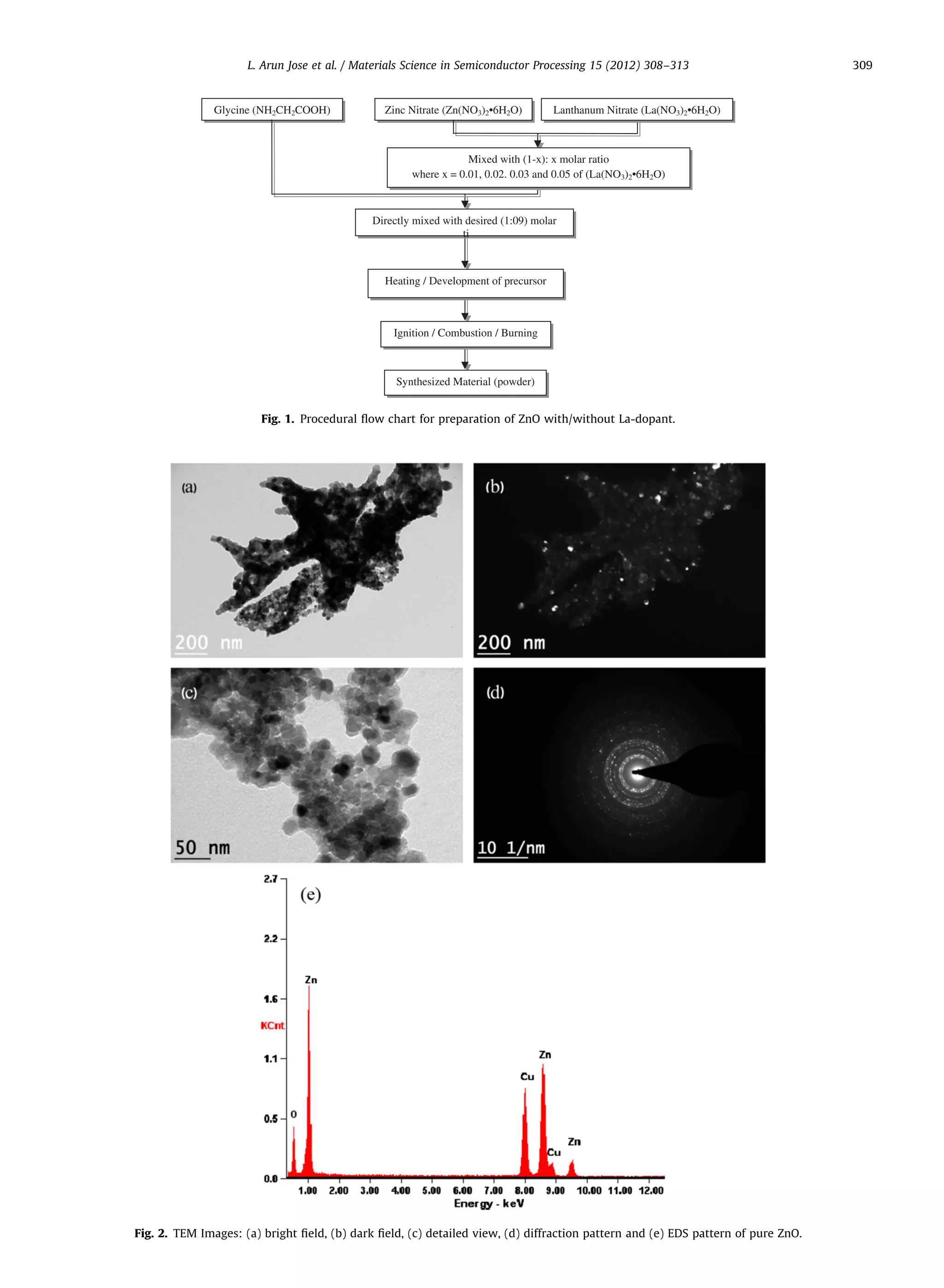
added to zinc nitrate with required molar ratio and glycine
2. Experimental details is also added along with it, in a molar ratio of 0.9:1 (zinc
nitrateþlanthanum nitrate:glycine) and stirred well for 1 h
Distinct from usual thermal evaporation, ZnO nano- in 100 ml double distilled water. The obtained solution is
structures were prepared by the combustion method, which heated ($185 1C) till combustion reaction occurs. Proce-
allows efficient synthesis of nano-size materials. This pro- dural flow chart diagram for the preparation of precursors
cess involves a self-sustained reaction in homogeneous and the formation of nano-structures is shown in Fig. 1.
solution of different oxidizers (e.g., metal nitrates) and fuels Crystallinity of pure ZnO and La-doped ZnO catalysts were
(e.g., urea, glycine, citric acid, hydrazides). Depending on the analyzed by Philips CM 20 Transmission Electron Micro-
type of precursors, and the suitable conditions for chemical scope which was operated between 20 and 200 kV. Com-
reaction to take place, zinc nitrate (Zn(NO3)2 Á 6H2O) was position of the samples were analyzed by energy dispersive
chosen as an oxidizer and glycine (NH2CH2COOH) as a fuel, X-ray spectroscopy (EDS) attached to the TEM instrument.
since its combustion heat (À3.24 kcal/g) is more negative X-ray diffraction patterns of the synthesized samples were
Fig. 3. TEM images: (a) bright field, (b) dark field, (c) detailed view, (d) diffraction pattern and (e) EDS pattern of 5 mol % La-doped ZnO.](https://image.slidesharecdn.com/opticalstudiesofnano-structuredla-dopedznopreparedbycombustionmethod-130209004543-phpapp01/75/Optical-studies-of-nano-structured-la-doped-zn-o-prepared-by-combustion-method-3-2048.jpg)
![L. Arun Jose et al. / Materials Science in Semiconductor Processing 15 (2012) 308–313 311
recorded using PAN analytical X-ray diffractometer with Cu
˚
Ka (1.5405 A) radiation in the scan range 2y between 301
and 701 with a scan speed of 21/min. UV–VIS spectra of pure
ZnO and La-doped ZnO catalysts were recorded using Varian
CARY 5E UV–VIS–NIR Spectrophotometer. The absorbance
spectra were then recorded in the range 200–700 nm.
Photoluminescence of pure ZnO and La-doped ZnO were
measured by Jobin Yvon Fluorolog spectrofluorometer and
the results are discussed in detail.
3. Results and discussion
TEM analysis shows that the nano-structures which
had been synthesized using combustion processing are
coral-shaped and porous as shown in Fig. 2. This shape
may be attributed to the thermal fluctuations while
synthesizing the samples. Grain size is found to be
$10–20 nm both in the case of pure and doped ZnO.
Porous nature of the nano-structures significantly increases
as the La-dopant concentration increases as shown in Fig. 3.
Fig. 4. Powder XRD spectra of samples pure–doped prepared at different
Each individual nano-structure is about 450–1000 nm mol percent of La.
formed by tiny spherical ZnO nanoparticles. We can also
notice that the pores are $ 10–50 nm in diameter which
considerably increase the surface to volume ratio. Selected even for the La-doped sample with a high La concentra-
area diffraction patterns match very well with wurtzite tion, suggesting that lanthanum oxide is uniformly dis-
ZnO in both pure and doped ZnO. EDS analysis shows that persed in the ZnO and no second phase such as La2O3 and
some La3 þ ions have been incorporated into the ZnO lattice La(OH)3 appears. It is evident that the introduction of La
by substituting zinc ions as shown in Fig. 3(e) and in ions does not alter the structure of ZnO and dopant
Table 1. When La is present the composition of oxygen disperses homogeneously in the ZnO matrix as previously
seems to be nearly constant. This may be due to the reported [37]. Using the Scherrer equations the crystallite
addition of oxygen atoms in the La-doped ZnO which was sizes were estimated to be around 450 nm from the full-
accommodated by the additional vacancy in the La3 þ ion. width at half-maximum (FWHM) of diffraction peaks. The
Copper peak in the EDS measurement originates from the diffraction pattern of ZnO is observed between the 2y
TEM supporting carbon coated copper grid. values of 301 and 701. The peak intensities of doped ZnO
XRD profiles of synthesized pure and doped materials increases with dopant concentration. Therefore, the crys-
in appropriate ratio are shown in Fig. 4. The diffraction talline nature of ZnO nanostructure increases with La-
peaks and their relative intensities match with the JCPDS dopant in the same manner as previously reported in the
card no. 36-1451. Hence the observed patterns can be case of Fe doped ZnO [38]. Doping of La ions restrains the
clearly endorsed to the presence of hexagonal wurzite growth of ZnO grains and dopant with smaller ionic
structure. XRD peak of lanthanum oxide was not observed radius has a constructive effect on diffusivity which
promotes orientation growth and good crystal [39]. The
lattice parameters and the unit cell volume were deter-
Table 1 mined using software program UnitCell method of TJB
Composition of elements in La-doped ZnO samples. Holland & SAT Redfern [40]. The determined unit cell
parameters, volume and c/a were plotted as a function of
La concentration (mol%) Element weight (%) Atomic (%)
La concentrations and are shown in Figs. 5 and 6 respec-
0 O 13.30 38.50 tively. The lattice constant gradually increases with
Zn 86.70 61.50 increase in concentration of La3 þ ions. Consequently, cell
1 O 20.30 51.73 volume and c/a ratio changed, agreeing with the fact that
La 04.34 01.27 ionic radii of La3 þ is higher than the Zn2 þ ion (0.106 nm
Zn 75.36 47.00 for La and 0.074 nm for Zn) [41,42] but there is a small
2 O 19.60 51.32 variation in c-axis compared with the results of Chen et al.
La 08.38 02.53 [37]. This distortion in the lattice parameters confirms the
Zn 72.02 46.15
incorporation of La3 þ ions up to 5 mol% in ZnO wurzite
3 O 18.94 50.92 structure.
La 12.15 03.76 UV–VIS spectrum shows that the absorbance is high
Zn 68.91 45.32
below 380 nm for pure ZnO and as the La-dopant con-
5 O 18.30 50.80 centration increases the absorbance of ZnO decreases
La 17.20 05.50
considerably below this region as shown in Fig. 7. The
Zn 64.50 43.70
corresponding band gap values of pure and doped ZnO are](https://image.slidesharecdn.com/opticalstudiesofnano-structuredla-dopedznopreparedbycombustionmethod-130209004543-phpapp01/75/Optical-studies-of-nano-structured-la-doped-zn-o-prepared-by-combustion-method-4-2048.jpg)
![312 L. Arun Jose et al. / Materials Science in Semiconductor Processing 15 (2012) 308–313
Fig. 5. Unit cell parameters a and c were plotted as a function of La
concentration.
Fig. 8. Calculated band gap of pure and La-doped ZnO.
Fig. 6. Unit cell volume and c/a were plotted as a function of La
concentration.
Fig. 9. Room temperature PL emission spectra of ZnO with/without
La-dopant.
less compared with La-doped ZnO and absorbance
increases with increase in dopant concentration.
Photoluminescence (PL) spectra of La-doped ZnO
nano-structures were measured with an excitation wave-
length of 285 nm and is shown in Fig. 9. The intensity of
PL emission is found to increase with increase in La-
dopant, but the intensity of doped ZnO decreases in
comparison with pure ZnO between 3.2 and 3.3 eV. The
PL spectrum shows the La characteristic emission band at
$ 2.9 eV and near UV emission between 3.27 and 3.30 eV.
There is a shift in the emission spectra for pure and doped
ZnO. This may be attributed due to the strain created in
the crystal lattice to accommodate larger La atoms.
Spectra in the range of 340–460 nm (2.7–3.6 eV) shows
Fig. 7. UV–VIS spectra ZnO with/without dopant. that a violet peak at about 420 nm (2.95 eV) and the
intensity of emission are found to be strongly reliant on
presented in Fig. 8. It can be clearly seen that the band gap the La concentration. Traps on the grain surface per unit
of La-doped ZnO also increases gradually with increase in volume increases with the increase of specific surface
La concentration. After 380 nm, absorbance of pure ZnO is area. Cordaro et al. [43] assumed that interface traps lie in](https://image.slidesharecdn.com/opticalstudiesofnano-structuredla-dopedznopreparedbycombustionmethod-130209004543-phpapp01/75/Optical-studies-of-nano-structured-la-doped-zn-o-prepared-by-combustion-method-5-2048.jpg)
![L. Arun Jose et al. / Materials Science in Semiconductor Processing 15 (2012) 308–313 313
the depletion regions and locate at the ZnO–ZnO grain [11] H. Huang, Y. Ou, S. Xu, G. Fang, M. Li, X. Zhao, Applied Surface
boundaries when a polycrystalline varistor forms, and the Science 254 (2008) 2013–2016.
[12] V. Zhitomirsky, E. Cetinorgu, R. Boxman, S. Goldsmith, Thin Solid
level of interface trap was found to be about 0.33 eV Films 516 (2008) 5079–5086.
below the conduction band edge. So violet emission is [13] T. Moriga, Y. Hayashi, K. Kondo, Y. Nishimura, K.-i. Murai,
possibly attributed to the recombination centers linked I. Nakabayashi, H. Fukumoto, K. Tominaga, Journal of Vacuum
Science and Technology A 22 (2004) 1705.
with interface traps existing at the grain boundaries, and [14] S. Saha, V. Gupta, AIP Advances 1 (2011) 042112.
radiative transition occurs between the level of interface [15] T.S. Herng, S.P. Lau, S.F. Yu, H.Y. Yang, K.S. Teng, J.S. Chen, Journal of
traps and the valence band. Physics: Condensed Matter 19 (2007) 356214.
´
[16] N.H. Hong, J. Sakai, V. Brize, Journal of Physics: Condensed Matter
19 (2007) 036219.
4. Conclusions [17] J. Zhang, X.Z. Li, J. Shi, Y.F. Lu, D.J. Sellmyer, Journal of Physics:
Condensed Matter 19 (2007) 036210.
[18] B. Li, X. Xiu, R. Zhang, Z. Tao, L. Chen, Z. Xie, Y. Zheng, Materials
La-doped ZnO was prepared by combustion proces-
Science in Semiconductor Processing 9 (2006) 141–145.
sing; doping levels included undoped, 1, 2, 3 and 5 molar [19] T. Gao, T.H. Wang, Applied Physics A 80 (2004) 1451–1454.
percentage. Significant transformation was observed upon [20] S. Anandan, A. Vinu, T. Mori, N. Gokulakrishnan, P. Srinivasu, V.
different doping concentrations. Transmission electron Murugesan, K. Ariga, Catalysis Communications 8 (2007)
1377–1382.
micrograph shows an enhancement of pore density for [21] Z.-X. Xu, V.A.L. Roy, P. Stallinga, M. Muccini, S. Toffanin, H.-F. Xiang,
doped ZnO. Lattice parameters and unit cell volume were C.-M. Che, Applied Physics Letters 90 (2007) 223509.
determined from the XRD data and it confirms the entry [22] C.-L. Hsu, T.-Y. Tsai, Journal of the Electrochemical Society 158
(2011) K20–K23.
of La-dopant inside ZnO crystal lattice by the increase in [23] Y.R. Ryu, J.A. Lubguban, T.S. Lee, H.W. White, T.S. Jeong, C.J. Youn,
lattice constants. It is evident that the absorbance near UV B.J. Kim, Applied Physics Letters 90 (2007) 131115.
region decreases with increase in dopant concentration. [24] X.M. Teng, H.T. Fan, S.S. Pan, C. Ye, G.H. Li, Journal of Applied
Physics 100 (2006) 053507.
The bandgap is found to increase with addition of La. The [25] S. Chirakkara, S.B. Krupanidhi, Physica Status Solidi RRL 6 (2012)
La-doped ZnO nano-structures prepared at low tempera- 34–36.
tures are more suitable for applications such as chemical [26] X. Chen, B. Xu, J. Xue, Y. Zhao, C. Wei, J. Sun, Y. Wang, X. Zhang,
X. Geng, Thin Solid Films 515 (2007) 3753–3759.
and biological sensors, optoelectronic devices, and
[27] P. Ruankham, T. Sagawa, H. Sakaguchi, S. Yoshikawa, Journal of
solar cells. Materials Chemistry 21 (2011) 9710–9715.
´
[28] S. Mendoza-Galvan, C. Trejo-Cruz, J. Lee, D. Bhattacharyya,
J. Metson, P.J. Evans, U. Pal, Journal of Applied Physics 99 (2006)
Acknowledgments 014306.
[29] I. Honma, S. Hirakawa, K. Yamada, J.M. Bae, Solid State Ionics 118
(1999) 29–36.
The authors gratefully acknowledge BRNS (Board of [30] M. Peres, A. Cruz, S. Pereira, M.R. Correia, M.J. Soares, A. Neves,
Research in Nuclear Sciences—Government of India, Pro- M.C. Carmo, T. Monteiro, A.S. Pereira, M.A. Martins, T. Trindade,
´
E. Alves, S.S. Nobre, R.A.Sa Ferreira, Applied Physics A 88 (2007)
ject no. 2008/37/12/BRNS/1513) for providing financial 129–133.
assistance. They are also thankful to authorities of Indian [31] S. Bachir, K. Azuma, J. Kossanyi, P. Valat, J.C. Ronfard-Haret, Journal
Institute of Technology, Chennai 36, for providing TEM, of Luminescence 75 (1997) 35–49.
[32] X.T. Zhang, Y.C. Liu, J.G. Ma, Y.M. Lu, D.Z. Shen, W. Xu, G.Z. Zhong,
UV–VIS, PL and powder XRD facility. X.W. Fan, Thin Solid Films 413 (2002) 257–261.
[33] G. Wu, Y. Zhuang, Z. Lin, X. Yuan, T. Xie, L. Zhang, Physica E
References 31 (2006) 5–8.
[34] S. Anandan, A. Vinu, K.L.P. Sheeja Lovely, N. Gokulakrishnan,
P. Srinivasu, T. Mori, V. Murugesan, V. Sivamurugan, K. Ariga,
[1] J.B. Varley, A. Janotti, C. Franchini, C.G. Van de Walle, Physical Journal of Molecular Catalysis A: Chemical 266 (2007) 149–157.
Review B 85 (2012) 081109. R. [35] C. Ge, C. Xie, M. Hu, Y. Gui, Z. Bai, D. Zeng, Materials Science and
[2] P.K. Sharma, R.K. Dutta, M. Kumar, P.K. Singh, A.C. Pandey, Journal Engineering: B 141 (2007) 43–48.
of Luminescence 129 (2009) 605–610. [36] C.-C. Hwang, T.-Y. Wu, Journal of Materials Science 39 (2004)
[3] J. Kennedy, D.A. Carder, A. Markwitz, R.J. Reeves, Journal of Applied 6111–6115.
Physics 107 (2010) 103518. [37] J.T. Chen, J. Wang, F. Zhang, G.A. Zhang, Z.G. Wu, P.X. Yan, Journal of
[4] H.-C. Shin, K.-R. Lee, S. Park, C.-H. Jung, S.-J. Kim, Japanese Journal of Crystal Growth 310 (2008) 2627–2632.
Applied Physics 35 (1996) L996–L998. [38] G.-Y. Ahn, S.-I. Park, S.-J. Kim, C.-S. Kim, Journal of Magnetism and
[5] F. Li, K. Hu, J. Li, D. Zhang, G. Chen, Journal of Nuclear Materials 300 Magnetic Materials 304 (2006) e498–e500.
(2002) 82–88. [39] S. Fujihara, C. Sasaki, T. Kimura, Journal of the European Ceramic
[6] L.E. Shea, J. McKittrick, O.A. Lopez, E. Sluzky, Journal of the Society 21 (2001) 2109–2112.
American Ceramic Society 79 (1996) 3257–3265. [40] T.J.B. Holland, S.A.T. Redfern, Journal of Applied Crystallography 30
[7] L. Chick, L. Pederson, G. Maupin, J. Bates, L. Thomas, G. Exarhos, (1997) 84.
Materials Letters 10 (1990) 6–12. [41] S.H. Jeong, B.N. Park, S.B. Lee, J.H. Boo, Surface and Coatings
[8] T. Mimani, K.C. Patil, Materials Physics and Mechanics 4 (2001) Technology 193 (2005) 340–344.
134–137. [42] Q. Yu, W. Fu, C. Yu, H. Yang, R. Wei, Y. Sui, S. Liu, Z. Liu, M. Li,
[9] R.D. Purohit, B.P. Sharma, K.T. Pillai, A.K. Tyagi, Materials Research G. Wang, C. Shao, Y. Liu, G. Zou, Journal of Physics D: Applied
Bulletin 36 (2001) 2711–2721. Physics 40 (2007) 5592.
[10] B.D. Ahn, S.H. Oh, C.H. Lee, G.H. Kim, H.J. Kim, S.Y. Lee, Journal of [43] J.F. Cordaro, Y. Shim, J.E. May, Journal of Applied Physics 60 (1986)
Crystal Growth 309 (2007) 128–133. 4186.](https://image.slidesharecdn.com/opticalstudiesofnano-structuredla-dopedznopreparedbycombustionmethod-130209004543-phpapp01/75/Optical-studies-of-nano-structured-la-doped-zn-o-prepared-by-combustion-method-6-2048.jpg)