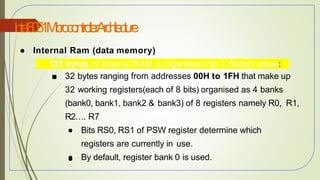
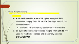
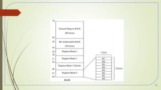
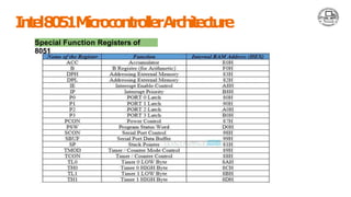
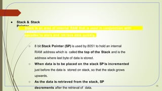
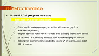
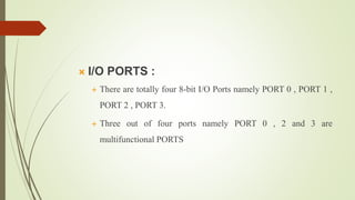
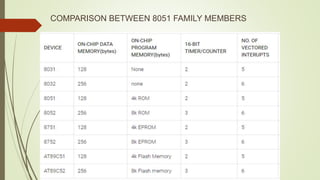
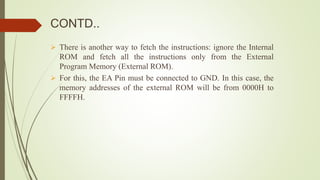
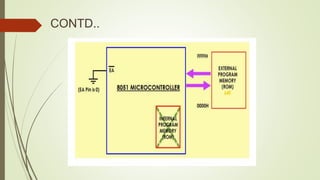
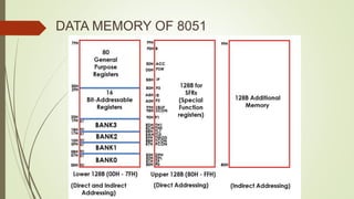
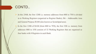
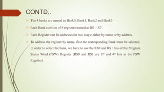
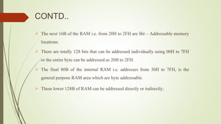
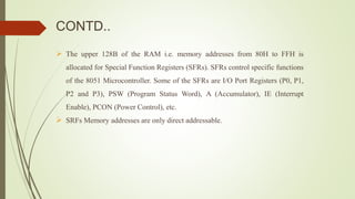
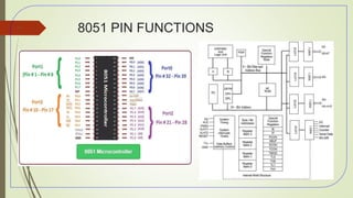
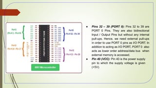
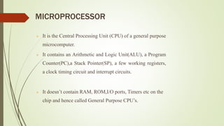
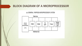
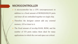
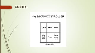
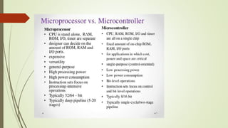
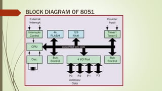
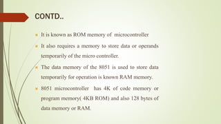
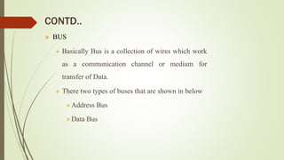
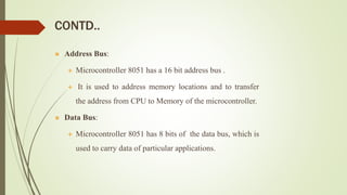
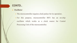
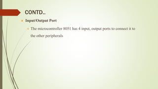
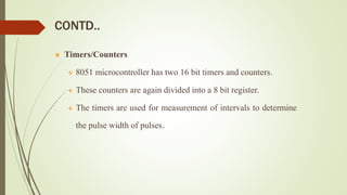
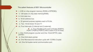
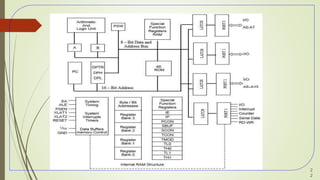
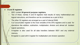
The document provides an overview of the functionalities and architecture of microcontrollers, particularly focusing on the 8051 microcontroller. It details the essential components such as the CPU, memory (RAM and ROM), I/O ports, timers, and interrupt sources, describing how they work together in a microcontroller system. The 8051 microcontroller features 4KB of program memory, 128 bytes of data memory, and multiple I/O capabilities, making it suitable for various applications where cost and space are critical.


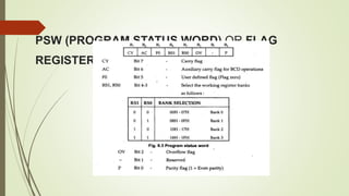
![ CY[Carry or Borrow Bit] = 1 indicates a CARRY has occurred out of
higher order nibble of accumulator or borrow has occurred into higher
order nibble of accumulator.
AC[Auxiliary Carry or Borrow Bit] = 1 indicates a CARRY has occurred
out of lower order nibble of accumulator or borrow has occurred into
lower order nibble of accumulator
F0 – General Purpose User Definable Flag](https://image.slidesharecdn.com/module1-240517154539-70ac0552/85/Microcontroller-Electronics-Engineering-Sem-4MODULE-1-pptx-26-320.jpg)
![ OV[Overflow or Sign] bit = 1 , Indicates the result in the
accumulator is a negative number in case of signed addition and the
result has exceeded the capacity of accumulator in case of unsigned
addition.
P[Parity] bit = 1 , indicates the result in the accumulator has ODD
PARITY.](https://image.slidesharecdn.com/module1-240517154539-70ac0552/85/Microcontroller-Electronics-Engineering-Sem-4MODULE-1-pptx-27-320.jpg)