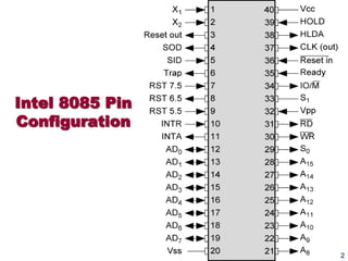
The document discusses the architecture and components of the Intel 8085 microprocessor. It includes:
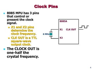
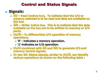
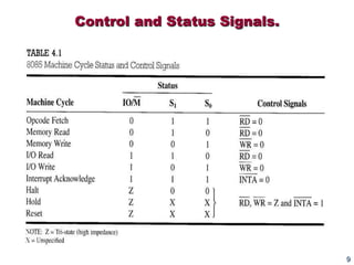
- Details on the 8085 clock pins, address bus, control and status signals, and interrupt pins.
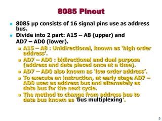
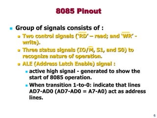
- An explanation of bus multiplexing which allows the AD0-AD7 pins to act as both the address bus and data bus.
- A diagram and description of the major components in the 8085 CPU including the registers, instruction decoder, ALU, and interrupt vectors.
- Explanations of the reset signals, direct memory access, and fetch-execute sequence through examples of MPU communication and bus timing diagrams.