Cu 2 ZnSnS 4 (CZTS) Thin Films for
Solar Cell Application
Dr. Ramesh J. Deokate
Vidya Pratishthan’s
Arts, Science and Commerce College,

Baramati
VPA SC

MS-413 133.
Outline of Presentation
Introduction of Cu2ZnSnS4(CZTS)
 Synthesis of Cu2ZnSnS4 Thin films
 Characterization techniques:
 X-ray diffraction (XRD )
Scanning Electron Microscopy (SEM)
Theromoemf power (TEP)
Resistivity measurement
 Contact angle and Band gap study

Conclusions
VPA SC
Properties of Cu2ZnSnS4 (CZTS)

VPA SC
Methodology
Advantages of SPT




Neither requires high quality targets
and/or substrates nor it requires
vacuum at any stage, which is a great
advantage if the technique is to be
scaled up for industrial applications.



The deposition rate and the thickness of
the films can be easily controlled over a
wide range by changing the spray
parameters.



Operating at moderate temperatures
(373-773 K), spray pyrolysis can
produce films on less robust materials.



It can be used to make layered films and
films having composition gradients
throughout the thickness.



VPA SC

Inexpensive, simple and convenient for
large area deposition.

This method provide one step synthesis
without no impurities.

Schematic representation of spray pyrolysis deposition apparatus
Preparation of Cu2ZnSnS4 films by Spray
pyrolysis technique
Chemicals used and preparative
parameters
Precursor solution

(Cd(CH3COO)2.2H2O) (0.025)
(Zn(CH3COO)2
SnCl4
4SC(NH2)2

Total quantity

80 ml

Deposition temp.

623 K

Deposition period

20 min.

Substrate

(0.025)
(0.025)
(0.2)

Glass

Reaction mechanism

VPA SC

2Cu(CH33COO)+ Zn(CH33COO)2+SnCl4+
2Cu(CH COO) + Zn(CH COO)2+ SnCl4+
8H22O+4SC(NH22)2→ Cu22ZnSnS4+4CO22↑+
8H O+ 4SC(NH )2 → Cu ZnSnS4+ 4CO ↑+
4CH33COOH↑+4NH44Cl↑+4NH3↑
4CH COOH↑+ 4NH Cl↑+4NH3↑
Film thickness measurements

Variation of Cu2ZnSnS4 film thickness for different solution quantity.

VPA SC

6
X-Ray diffraction (XRD) studies

VPA SC
Scanning Electron Micrograph (SEM)

VPA SC
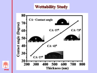
Wettability Study

VPA SC
Optical study and Electrical Resistivity
Increasing film thickness
the band gap energy
the band gap energy
increases from 1.59 to 1.67
eV.
eV.

4.0
log ρ (Ω−cm)

3.6

The resistivity decreases with
increase in temperature which
is the indication of typical

244 nm
375 nm
568 nm
754 nm

semiconductor characteristic..
semiconductor characteristic

3.2
2.8
2.4
2.0

VPA SC

1.0

1.5

2.0

2.5

3.0

-1

1000/T (K )

3.5

4.0
Summary and conclusions
 The CZTS thin films have been successfully deposited by a simple
and inexpensive spray pyrolysis technique.
 The thickness of CZTS films affects structural, optical and electrical
properties.
 The crystallinity and the grain size increased with film thickness.
Optical absorption study revealed indirect direct transition with
band gap energy in the range 1.6 to 1.67 eV, depending on film
thickness.
 The electrical conductivity and contact angle were enhanced with
the film thickness.

VPA SC
Acknowledgement
Authors are grateful to University of Pune
(UoP) for financial support through the BCUD
scheme no. 36-207/2012-14 (SR).

VPA SC
Thank You

VPA SC

305 deokate

  • 1.
    Cu 2 ZnSnS4 (CZTS) Thin Films for Solar Cell Application Dr. Ramesh J. Deokate Vidya Pratishthan’s Arts, Science and Commerce College, Baramati VPA SC MS-413 133.
  • 2.
    Outline of Presentation Introductionof Cu2ZnSnS4(CZTS)  Synthesis of Cu2ZnSnS4 Thin films  Characterization techniques:  X-ray diffraction (XRD ) Scanning Electron Microscopy (SEM) Theromoemf power (TEP) Resistivity measurement  Contact angle and Band gap study Conclusions VPA SC
  • 3.
  • 4.
    Methodology Advantages of SPT   Neitherrequires high quality targets and/or substrates nor it requires vacuum at any stage, which is a great advantage if the technique is to be scaled up for industrial applications.  The deposition rate and the thickness of the films can be easily controlled over a wide range by changing the spray parameters.  Operating at moderate temperatures (373-773 K), spray pyrolysis can produce films on less robust materials.  It can be used to make layered films and films having composition gradients throughout the thickness.  VPA SC Inexpensive, simple and convenient for large area deposition. This method provide one step synthesis without no impurities. Schematic representation of spray pyrolysis deposition apparatus
  • 5.
    Preparation of Cu2ZnSnS4films by Spray pyrolysis technique Chemicals used and preparative parameters Precursor solution (Cd(CH3COO)2.2H2O) (0.025) (Zn(CH3COO)2 SnCl4 4SC(NH2)2 Total quantity 80 ml Deposition temp. 623 K Deposition period 20 min. Substrate (0.025) (0.025) (0.2) Glass Reaction mechanism VPA SC 2Cu(CH33COO)+ Zn(CH33COO)2+SnCl4+ 2Cu(CH COO) + Zn(CH COO)2+ SnCl4+ 8H22O+4SC(NH22)2→ Cu22ZnSnS4+4CO22↑+ 8H O+ 4SC(NH )2 → Cu ZnSnS4+ 4CO ↑+ 4CH33COOH↑+4NH44Cl↑+4NH3↑ 4CH COOH↑+ 4NH Cl↑+4NH3↑
  • 6.
    Film thickness measurements Variationof Cu2ZnSnS4 film thickness for different solution quantity. VPA SC 6
  • 7.
  • 8.
  • 9.
  • 10.
    Optical study andElectrical Resistivity Increasing film thickness Increasing film thickness the band gap energy the band gap energy increases from 1.59 to 1.67 increases from 1.59 to 1.67 eV. eV. 4.0 log ρ (Ω−cm) 3.6 The resistivity decreases with The resistivity decreases with increase in temperature which increase in temperature which is the indication of typical is the indication of typical 244 nm 375 nm 568 nm 754 nm semiconductor characteristic.. semiconductor characteristic 3.2 2.8 2.4 2.0 VPA SC 1.0 1.5 2.0 2.5 3.0 -1 1000/T (K ) 3.5 4.0
  • 11.
    Summary and conclusions The CZTS thin films have been successfully deposited by a simple and inexpensive spray pyrolysis technique.  The thickness of CZTS films affects structural, optical and electrical properties.  The crystallinity and the grain size increased with film thickness. Optical absorption study revealed indirect direct transition with band gap energy in the range 1.6 to 1.67 eV, depending on film thickness.  The electrical conductivity and contact angle were enhanced with the film thickness. VPA SC
  • 12.
    Acknowledgement Authors are gratefulto University of Pune (UoP) for financial support through the BCUD scheme no. 36-207/2012-14 (SR). VPA SC
  • 13.