Use pspice for behavioral modeling of VCOs, EDN 2002
1. 102 edn | December 12, 2002 www.edn.com
ideas
design
P
Spice, a member of the Spice fam-
ily for PC users,is becoming
a standard tool for analog
and mixed analog-digital simulation.
Many analog designers are familiar with
the software of Design Center, Design
Lab, and OrCad (www.orcad.com)
PSpice and use the software in their
everyday lives. This Design Idea should
be helpful to those who design and sim-
ulate PLL systems at a behavioral level.A
basic PLL system comprises a phase de-
tector, a loop filter, and a VCO (voltage-
controlled oscillator), connected in a
negative-feedback loop. The phase de-
tector produces a voltage that, after low-
pass-filtering by the loop filter, becomes
an error voltage, VE
, applied to the con-
trol input of theVCO to set the an-
gular frequency,().WhenVE
ϭ0,
the VCO oscillates at some initial fre-
quency, 0
, called the frequency offset or
free-running frequency. The output
frequency of the VCO is:
(t)ϭ0
ϩGVCO
VE
(t).
Here,
where GVCO
is the VCO’s voltage-to-radi-
an frequency gain in radians per second
per volt and gVCO
is theVCO’s voltage-to-
frequency gain in hertz per volt. Consid-
er a sinusoidal voltage with amplitude
VAMPL
, argument (t), and dc offset VOFF
:
The argument (t) is the time integral of
the angular frequency:
Assuming is constant and substituting
(t) in V(t) yields the popular form:
If is not constant, the general form is:
Replacing (t) with Equation1 and con-
sidering (0)ϭ0, you obtain the VCO’s
transfer function:
Use PSpice for behavioral modeling of VCOs
Dobromir Dobrev, Jet Electronics, Sofia, Bulgaria
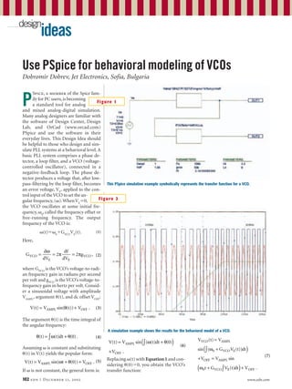
Figure 1
This PSpice simulation example symbolically represents the transfer function for a VCO.
A simulation example shows the results for the behavioral model of a VCO.
Figure 2
G
d
dV
df
dV
gVCO
E E
VCO= = =
ω
π π2 2 , (2)
(1)
V t V t VAMPL OFF( ) sin( ( )) .= +θ (3)
θ ω θ( ) ( ) ( ) .t t dt= +∫ 0 (4)
V t V t VAMPL OFF( ) sin( ( )) .= + +ω θ 0 (5)
V t V t dt
V
AMPL
OFF
( ) sin ( ( ) ( )
.
= +( )
+
∫ ω θ 0
(6)
V t V
G V t dt
V V
t G V
VCO AMPL
VCO E
OFF AMPL
VCO
( )
sin ( ( ))
sin
=
+( )
+ =
+
∫ ω
ω
0
0 EE OFFt dt V( ) .∫( )+
(7)
2. 104 edn | December 12, 2002 www.edn.com
ideas
design
Equation 7 is the heart of the VCO’s
time-analysis modeling. Thus, you can
easily perform VCO behavioral model-
ing, using the ABM1 part from the Ana-
log Behavioral Modeling Symbol Library
abm.slb (abm.olb in OrCad Capture).
You can simply write the formula for the
transfer function, adapted for PSpice.
Figure1 shows the PSpice representation
of the process. Figure 2 shows a simula-
tion example, in which VE
is the VCO’s
input voltage, and V(OUT1)
is the output
voltage. Because most phase detectors
(types I,II,and III) use a digital input sig-
nal, you can easily obtain a digital VCO-
output waveform using the conditional
expression above the lower box in Figure
1. The simulated curve is V(OUT2)
, also
shown in Figure 2. Finally, for loop-gain
evaluation in ac analysis, you simply
model theVCO in the frequency domain
in an ideal integrating unit, using the
Laplace form TVCO
(s)ϭGVCO
/s. Most ob-
vious behavioral VCO models are based
on a real circuit concept.Thus,they com-
prise many elements—for example, con-
trollable sources, capacitors, and others.
Hence, the models are complicated. This
modeling is simple without involving su-
perfluous computation resources.
Is this the best Design Idea in this
issue? Select at www.edn.com.
T
he need for higher voltage swings
in applications such as test-and-
measurement instruments is con-
stantly increasing,but the power supplies
impose limitations on the operational
amplifier rails make the high-voltage
need a challenge for designers. How do
you deliver high-voltage swings to a load
without increasing the voltage levels of
the power supplies of the operational
amplifier? In other words, for example,
how can you produce a Ϯ16V or greater
signal swing across the load using only
Ϯ15V power supplies? The circuit in Fig-
ure 1 uses a fully differential amplifier to
offer an answer to this problem.Fully dif-
ferential amplifiers enable you to deliver
an output-voltage swing beyond the rails
into the load. One of the common prob-
lems in working with operational ampli-
fiers is the limit that the power-supply
rails impose. The standard since the days
of analog computers has been Ϯ15V.
Analog computers are gone, but their
legacy remains in the power-supply volt-
ages. These voltages find widespread use
in transducer interfaces and applications
in which voltage swing and dynamic
range are of primary importance.
This Ϯ15V supply voltage notwith-
standing,applications exist that require a
higher swing range beyond the power-
supply limits. Typical Ϯ15V operational
amplifiers are seldom optimized for rail-
to-rail operation, and their useful out-
put-voltage range may be only 24 to 26V.
Many audio consoles use older technol-
ogy 741 op amps with Ϯ18, Ϯ20, and
even Ϯ22V power supplies to obtain
more voltage swing and, therefore, more
dynamic range from their systems in light
of this limitation. The op amps in these
systems often run hot and have heat
sinks. The advent of fully differential op
amps has given designers a better way to
extend the output-swing range.Fully dif-
ferential operational amplifiers 40 to 50
years ago were tube or discrete-transistor
units.They have recently re-emerged as a
way to interface to fully differential A/D
converters and applications in which the
load needs differential drive for better
swing range or to reduce the noise effects
in the systems.
The outputs of fully differential op
amps have a characteristic that makes
them useful for doubling the swing. The
two outputs are 180Њ out of phase: When
one output swings positive, the other
swings negative and vice versa.The net ef-
fect is similar to what happens in a
bridged amplifier: The effective output-
voltage range doubles. The price of dou-
bling this output-voltage swing is that you
can no longer connect the output load to
ground. Designers of automotive audio
amplifiers are familiar with this concept:
Audio-power bridged amplifiers have a
fully differential output. Many installers
have learned the hard way that the minus
speaker connection cannot connect to
ground. When the output voltage dou-
bles, power quadruples. This feature is
useful for audio power amplifiers in a lim-
ited-power-supply-voltage application.
To illustrate the advantage of fully dif-
ferential outputs, assume that a fully dif-
ferential op amp has a voltage-rail limi-
tation of Ϯ13V when operated from
Ϯ15V supplies.The absolute- maximum
output range of each output is Ϯ13V.But
when the top output is at 13V,the bottom
output is Ϫ13V: (13V)Ϫ(Ϫ13V)ϭ26V.
When the top output is Ϫ13V, the bot-
tom output is 13V. As a result, the out-
put voltage is (Ϫ13V)Ϫ(13V)ϭϪ26V.
Therefore, the output-voltage range is
Circuit delivers high voltage swing
from lower supplies
Bruce Carter and Ron Shakery, Texas Instruments, Dallas, TX