SlideShare a Scribd company logo
Introduction to Sequential
Design
Types of Logic Circuits
 Logic circuits can be:
 Combinational Logic Circuits-outputs
depend only on current inputs
 Sequential Logic Circuits-outputs
depends not only on current inputs but
also on the past sequence of inputs
Sequential Circuit Models
Combinational Logic Delay
A
B
C
D
Y
5ns
5ns
5ns
5ns
5ns
Shortest delay
Longest delay
Longest timing delay = 5ns+5ns+5ns+5ns = 20ns
Shortest timing delay = 5ns
We will use the longest delay to represent the combinational logic (CL) delay, tcl
Combinational Logic (CL)
Cloud Model
A
B
C
D
E
Y
5ns
5ns
5ns
5ns
5ns
CL
tcl
Tcl=20ns
Tcl=20ns
Memory
Memory
 We will add memory (or
registers) to our logic circuits.
This will allow us to design
sequential circuits.
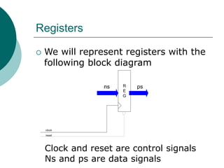
Registers
 We will represent registers with the
following block diagram
R
E
G
ps
ns
clock
reset
Clock and reset are control signals
Ns and ps are data signals
Sequential Systems
Block Diagrams
Sequential Systems
General Block Diagram
R
E
G
CL
F
CL
H Y
ps
ns
X
clock
reset
Input Vector
Output Vector
Next
State
Present
State
Feedback
Path
CL= Combinational Logic Cloud
Reg= D Registers
Clock
Reset
Sequential Systems
General Block Diagram
R
E
G
CL
F
CL
H Y
ps
ns
X
clock
reset
Input Vector
Output Vector
Next
State
Present
State
Feedback
Path
Clock
Reset
X is the input data vector
Y is the output data vector
Sequential Systems
Block Diagram
R
E
G
CL
F
CL
H Y
ps
ns
X
clock
reset
Input Vector
Output Vector
Next
State
Present
State
Feedback
Path
Clock
Reset
Ns is the next state data vector
Ps is the present state data vector
Sequential Systems
Block Diagram
R
E
G
CL
F
CL
H Y
ps
ns
X
clock
reset
Input Vector
Output Vector
Next
State
Present
State
Feedback
Path
Clock
Reset
Notice we have a feedback path which
combines the ps data vector with the
input vector to generate a new ns data
vector.
Sequential Systems
Block Diagram
R
E
G
CL
F
CL
H Y
ps
ns
X
clock
reset
Input Vector
Output Vector
Next
State
Present
State
Feedback
Path
Clock
Reset
 
 
,
s s
s
n F X p
Y H p


Mathematically, we say
Or, ns is a function F of X and ps
and Y is a function H of ps.
Example
Circuit Schematic
F Logic Register
H Logic
(buffer)
R
E
G
CL
F
CL
H Y
ps
ns
X
clock
reset
X input ns ps
Block Diagram
Example
Circuit Schematic
F Logic Register
H Logic
(buffer)
X input ns ps
State Equations
s s s
s
n J p K p
Y p
 

Finite State Machine (FSM)
General Models
Moore FSM
General Block Diagram
R
E
G
CL
F
CL
H Y
ps
ns
X
clock
reset
Input Vector
Output Vector
Next
State
Present
State
Feedback
Path
CL= Combinational Logic Cloud
Reg= D Registers
Clock
Reset
Moore FSM
State Equations
R
E
G
CL
F
CL
H Y
ps
ns
X
clock
reset
Input Vector
Output Vector
Next
State
Present
State
Feedback
Path
Clock
Reset
 
 
,
s s
s
n F X p
Y H p


State Equations
R
E
G
CL
F
CL
H Y
ps
ns
X
clock
reset
Mealy FSM
Block Diagram and State Equations
 
 
,
,
s s
s
n F X p
Y H X p


Input Vector Output Vector
Next
State
Present
State
Feedback
Path
Output Y is also a function
of input X
R
E
G
CL
F
CL
H1
Y1
ps
ns
X
clock
reset
Y2
CL
H2
Mealy-Moore FSM
Block Diagram and State Equations
 
   
1 1 2 2
,
,
s s
s s
n F X p
Y H X p Y H p

 
Input Vector
Next State Present State
Mealy Outputs
Moore Outputs
State Diagrams
State Bubble
Name
[Value]
Output
[Conditional]
State
(transition)
State Bubble Example
S0
00
Y=0
upn
upn
Unconditional
Transition
State name = S0
State value = 00
Y = 0 for this state
Conditional
Transition
We leave this state if upn=1,
We remain in this state if upn=0
Memory Devices
Memory Devices
 Data Latch (D-latch)
 Flip-flops (edge triggered)
 D-FF, D Register
 JK-FF
 T-FF
D-FF Positive Edge Triggered
Block Diagram
Q
Q
SET
CLR
D
Qn+1
D
Clk
Pre
Rst
Symbol
4 inputs: D,Clk,Pre,Rst
One output: Q
D = Data Input
Clk = Clock Input
Pre = Preset Input
Rst = Reset Input
D-FF Truth Table
Q
Q
SET
CLR
D
Qn+1
D
Clk
Pre
Rst
D Clk
d d 1 0 0
d d 0 1 1
d 0 1 1
d 1 1 1
0 1 1 0
1 1 1 1
Symbol
Equation (rising clock)
Truth Table
Pre Rst 1
n
Q 
n
Q
n
Q


1
n n
Q D
 
D-FF Truth Table
Q
Q
SET
CLR
D
Qn+1
D
Clk
Pre
Rst
D Clk
d d 1 0 0
d d 0 1 1
d 0 1 1
d 1 1 1
0 1 1 0
1 1 1 1
Symbol
Equation (rising clock)
Truth Table
Pre Rst 1
n
Q 
n
Q
n
Q


1
n n
Q D
 
Pre= Preset Input (active low)
Rst = Reset Input (active low)
Highest priority
D-FF Truth Table
Q
Q
SET
CLR
D
Qn+1
D
Clk
Pre
Rst
D Clk
d d 1 0 0
d d 0 1 1
d 0 1 1
d 1 1 1
0 1 1 0
1 1 1 1
Symbol
Equation (rising clock)
Truth Table
Pre Rst 1
n
Q 
n
Q
n
Q


1
n n
Q D
 
D = Data Input
Clk = Clock input
Qn = Register Output
FSM Examples
Example– 2-bit Up Counter
 State Diagram
S0
s3
S2
S1
Reset
Y=0
Y=1
Y=2
Y=3
Clock is implied
Example – 2-bit Up Counter
 State Table
ps ns y
S0 S1 0
S1 S2 1
S2 S3 2
S3 S0 3
S0 = 00
S1 = 01
S2 = 10
S3 = 11
Let
Let S0 = reset state
State Value Assignment
Output
Vector
Example – 2-bit Up Counter
 Truth Table
ps1 ps0 ns1 ns0 y1 y0
0 0 0 1 0 0
0 1 1 0 0 1
1 0 1 1 1 0
1 1 0 0 1 1
Example – 2-bit Up Counter
 Excitation
Equations
1 1 0
0 0
1 1
0 0
s s s
s s
s
s
n p p
n p
Y p
Y p
 



Moore FSM
R
E
G
CL
F
CL
H Y
ps
ns
X
clock
reset
Input Vector
Output Vector
Next
State
Present
State
Feedback
Path
Clock
Reset
 
 
,
s s
s
n F X p
Y H p


State Equations
Logic Diagram
F Logic
H Logic
Reg Block
Y Vector
No X Vector in this Example
No H Logic needed
Logic Diagram
Flash Animation
Example 3– 2-bit Down Counter
 State Diagram
S0
s3
S2
S1
Reset
Y=0
Y=1
Y=2
Y=3
Clock is implied
Example – 2-bit Down Counter
 State Table
ps ns y
S0 S3 0
S3 S2 3
S2 S1 2
S1 S0 1
S0 = 00
S1 = 01
S2 = 10
S3 = 11
Let
Let S0 = reset state
Example – 2-bit Down Counter
 Truth Table
ps1 ps0 ns1 ns0 y1 y0
0 0 1 1 0 0
0 1 0 0 0 1
1 0 0 1 1 0
1 1 1 0 1 1
Example – 2-bit Down Counter
 Excitation
Equations
1 1 0
0 0
1 1
0 0
s s s
s s
s
s
n p p
n p
Y p
Y p
 



Recall Moore FSM
R
E
G
CL
F
CL
H Y
ps
ns
X
clock
reset
Input Vector
Output Vector
Next
State
Present
State
Feedback
Path
Clock
Reset
 
 
,
s s
s
n F X p
Y H p


State Equations
Logic Diagram
F Logic
H Logic
Reg Block
Y Vector
No X Vector in this Example
Logic Diagram
Example 4 –
2-bit Up/Down Counter
 State Diagram
S0
s3
S2
S1
Reset
upn
upn
upn
upn
upn
upn
upn
upn
Example –
2-bit Up/Down Counter
 State Diagram
S0
s3
S2
S1
Reset
upn
upn
Shorthand Notation
Example – 2-bit Up/Down Counter
 State Table
ps ns
upn
ns
upn
y
S0 S1 S3 0
S1 S2 S0 1
S2 S3 S1 2
S3 S0 S2 3
S0 = 00
S1 = 01
S2 = 10
S3 = 11
Let
Let S0 = reset state
Example –
2-bit Up/Down Counter
 Truth Table
upn ps1 ps0 ns1 ns0 y1 y0
0 0 0 0 1 0 0
0 0 1 1 0 0 1
0 1 0 1 1 1 0
0 1 1 0 0 1 1
1 0 0 1 1 0 0
1 0 1 0 0 0 1
1 1 0 0 1 1 0
1 1 1 1 0 1 1
Example – 2-bit Up/Down Counter
 Excitation
Equations
1 1 0
0 0
1 1
0 0
s s s
s s
s
s
n p p upn
n p
Y p
Y p
  



Recall Moore FSM
R
E
G
CL
F
CL
H Y
ps
ns
X
clock
reset
Input Vector
Output Vector
Next
State
Present
State
Feedback
Path
Clock
Reset
 
 
,
s s
s
n F X p
Y H p


State Equations
Logic Diagram
X Vector
Y Vector
F Logic
H Logic
Reg Block
Logic Diagram
Example 5– 3-bit Arbitrary Counter
 Design a 3-bit arbitrary counter that will
count in the following sequence
3,2,3,1,2,3
If a state is not used reset it to state zero.
• How may states do we have?
• How many registers do we need?
• How many bits do we need for Y?
Example 5– 3-bit Arbitrary Counter
 State Diagram
S0
s3 S2
S1
Reset
Y=3
Y=2
Y=3
Y=1
s4
Y=2
S5
S6
S7
Y=0
Example – Arbitrary 3-bit Counter
 State Table
ps ns y
S0 S1 3
S1 S2 2
S2 S3 3
S3 S4 1
S4 S0 2
S5 S0 0
S6 S0 0
S7 S0 0
S0 = 000
S1 = 001
S2 = 010
S3 = 011
S4 = 100
S5 = 101
S6 = 110
S7 = 111
Let
Let S0 = reset state
Assign State Values
Develop Truth Table
Ps2 Ps1 Ps0 ns2 ns0 ns1 Y Y1 Y0
0 0 0 0 0 1 3 1 1
0 0 1 0 1 0 2 1 0
0 1 0 0 1 1 3 1 1
0 1 1 1 0 0 1 0 1
1 0 0 0 0 0 2 1 0
1 0 1 0 0 0 0 0 0
1 1 0 0 0 0 0 0 0
1 1 1 0 0 0 0 0 0
Example – 2-bit Arbitrary Counter
 Develop Excitation Equations -- F Logic
 
2 2 1 0
1 2 1 0
0 2 0
s s s s
s s s s
s s s
n p p p
n p p p
n p p

 

Develop Excitation Equations for Y
00 01 11 10
0 1 1 1
1 1
00 01 11 10
0 1 1 1
1
Y1
Y0
Example – 2-bit Arbitrary Counter
 Excitation Equations -- H Logic
 
 
1 2 1 0 1 0
0 2 1 0
s s s s s
s s s
y p p p p p
y p p p
  
 
Recall Moore FSM
R
E
G
CL
F
CL
H Y
ps
ns
X
clock
reset
Input Vector
Output Vector
Next
State
Present
State
Feedback
Path
Clock
Reset
 
 
,
s s
s
n F X p
Y H p


State Equations
Logic Circuit
F
H
R
E
G
Logic Circuit
Simulation
Example 5– 2-bit Up/Down Counter with Active Low Enable and
Synchronous RESET (SRESET)
 State Diagram
Clock is implied S0
s3
S2
S1
Resetn
upn en srn
en srn
upn en srn
en srn
en srn
upn en srn
upn en srn
srn
upn en srn
upn en srn
srn
upn en srn
upn en srn
en srn
Example – 2-bit Up/Down Counter with
Enable and SRESET
 Functional Table
srn en upn Function
0 d d Synchronous Reset (sreset)
1 1 d Hold
1 0 0 Count Up
1 0 1 Count Down
Highest Level of Priority Lowest Level of Priority
State Table
Srn En up
n
ns
0 d d S0
1 1 d ps
1 0 0 ps+1
1 0 1 ps -1
Truth Table (5 variables!!)
Srn En Upn Ps1 Ps0 Ns0 Ns1 # of Rows
0 d d d d 0 0 16
1 1 d Ps1 Ps0 Ps1 Ps0 8
1 0 0 0 0 0 1 1
1 0 0 0 1 1 0 1
1 0 0 1 0 1 1 1
1 0 0 1 1 0 0 1
1 0 1 0 0 1 1 1
1 0 1 0 1 0 0 1
1 0 1 1 0 0 1 1
1 0 1 1 1 1 1 1
32
Although, we could design this circuit directly from the truth table
we will use design partitioning.
Moore FSM Architecture
R
E
G
CL
F
CL
H Y
ps
ns
X
clock
reset
Input Vector
Output Vector
Next
State
Present
State
Feedback
Path
 
 
,
s s
s
n F X p
Y H p


Partitioned Design
Mux
Y
MUX
A
2
A
1
A
0
A
3
S1
R
E
G
CL
H Y
ps
ns
clock
en
S0
srn
"0"
"0"
ps
reset
UP/Down
Logic
Upn
Note, with the partitioned design we can “reuse” already designed submodules
to create the “new” design.
Srn En ns
0 d S0
1 1 PS
1 0 Count
We have
srn
en
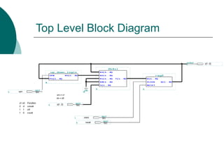
Top Level Block Diagram
UP/Down Logic
Symbol
Logic Circuit
Register Block
Symbol
Logic Circuit
2 Bit 4x1 Mux
Symbol
Circuit
1-bit 4x1 Mux
Symbol
Logic Circuit
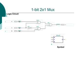
1-bit 2x1 Mux
Symbol
Logic Circuit
Top Level Block Diagram
Simulation
Example 6 – FSM Controller
State Diagram
S0
S1
S2
S3
reset=0
T
T
T
3
2
1
0
T
Truth Table for NS
Ps1 Ps0 T NS1 Ns0 Y1 Y0
0 0 0 0 1 0 0
0 0 1 0 1 0 0
0 1 0 1 0 0 1
0 1 1 0 1 0 1
1 0 0 1 1 1 0
1 0 1 0 0 1 0
1 1 0 1 0 1 1
1 1 1 1 0 1 1
Truth Table
S0
S1
S2
S3
reset=0
T
T
T
3
2
1
0
T
Kmaps for NS1 and NS0
P1P0
T
00 01 11 10
0 1 1 1
1 1
NS1
1 0 1 1 0
s s s s
ns T p T p p p
  
P1P0
T
00 01 11 10
0 1 1
1 1 1
NS0
0 1 0 1 0
s s s s
ns T p T p p p
  
Truth Table and Equations for Y
Ps1 Ps0 Y1 Y0
0 0 0 0
0 1 0 1
1 0 1 0
1 1 1 1
Truth Table
1 1 0 0
;
Y PS Y PS
 
By Inspection
Recall, Moore FSM, so Y will
Not be a function of T
Logic Circuit
F
H
R
E
G
Simulation
Memory Devices
Flip-Flops
D-FF Truth Table
Qn follows D on Rising Edge of CLK
Q
Q
SET
CLR
D
Qn+1
D
Clk
Pre
Rst
D Clk
d d 1 0 0
d d 0 1 1
d 0 1 1
d 1 1 1
0 1 1 0
1 1 1 1
Symbol
Equation (rising clock)
Truth Table
Pre Rst 1
n
Q 
n
Q
n
Q


1
n n
Q D
 
D = Data Input
Clk = Clock input
Qn = Register Output
T-FF (Toggle)
Changes state on every tick of CLK
T Clk
D d 1 0 0
D d 0 1 1
d 0 1 1
d 1 1 1
0 1 1
1 1 1
Symbol
Equation (rising clock)
Truth Table
Pre Rst 1
n
Q 
n
Q
n
Q


1
n n n
Q TQ TQ
  
T
Clk
Pre
Rst
Q
Q
SET
CL
R
T
Qn+1
n
Q
n
Q
SR-FF
Set =>Qn=1
Reset=>Qn=0
S R Clk
d d d 1 0 0
d d d 0 1 1
d d 0 1 1
d d 1 1 1
0 0 1 1
0 1 1 1 0
1 0 1 1 1
1 1 1 1 ???
n
Q
Symbol
Equation (rising clock)
Truth Table
Pre Rst 1
n
Q 
n
Q




n
Q
Rst
Q
Q
SET
CLR
S
R
S
Clk
R
Pre
Qn+1
1
n n
Q SRQ SR
  
JK-FF
J K Clk
d d d 1 0 0
d d d 0 1 1
d d 0 1 1
d d 1 1 1
0 0 1 1
0 1 1 1 0
1 0 1 1 1
1 1 1 1
n
Q
Symbol
Equation (rising clock)
Truth Table
Pre Rst 1
n
Q 
n
Q


1
n n n
Q JQ KQ
  


n
Q
n
Q
Rst
J
Q
Q
K
SET
CLR
J
Clk
K
Pre
Qn+1
Example: Design a JK-FF using
only Logic and a D-FF
J K Clk
d d d 1 0 0
d d d 0 1 1
d d 0 1 1
d d 1 1 1
0 0 1 1
0 1 1 1 0
1 0 1 1 1
1 1 1 1
n
Q
Symbol
Truth Table
Pre Rst 1
n
Q 
n
Q




n
Q
n
Q
Rst
J
Q
Q
K
SET
CLR
J
Clk
K
Pre
Qn+1
Example
S0 S1
Reset
0 1
J K
J
K
J K PS NS Y
0 0 S0 S0 0
0 0 S1 S1 1
0 1 S0 S0 0
0 1 S1 S0 1
1 0 S0 S1 0
1 0 S1 S1 1
1 1 S0 S1 0
1 1 S1 S0 1
State Diagram State Table
Let s0=0 and s1=1
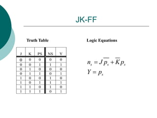
JK-FF
J K PS NS Y
0 0 0 0 0
0 0 1 1 1
0 1 0 0 0
0 1 1 0 1
1 0 0 1 0
1 0 1 1 1
1 1 0 1 0
1 1 1 0 1
Truth Table
s s s
s
n J p K p
Y p
 

Logic Equations
Recall Moore FSM
State Equations
R
E
G
CL
F
CL
H Y
ps
ns
X
clock
reset
Input Vector
Output Vector
Next
State
Present
State
Feedback
Path
Clock
Reset
 
 
,
s s
s
n F X p
Y H p


State Equations
JK Example
Circuit Schematic
F Logic D-Register
H Logic
(buffer)
R
E
G
CL
F
CL
H Y
ps
ns
X
clock
reset
X input ns ps
Block Diagram
JK Example
Circuit Schematic Simulation
Latches
D-Latch Block Diagram
Symbol
D
E
Pre
Rst
Q
Q
SET
CLR
D
E
Qn+1
4 inputs: D,E,Pre,Rst
One output: Q
D = Data Input
E = Enable Input
Pre = Preset Input
Rst = Reset Input
D-Latch
Truth Table
D E
d d 1 0 0
d d 0 1 1
d 0 1 1
0 1 1 1 0
1 1 1 1 1
Symbol Truth Table
Pre Rst 1
n
Q 
n
Q
D
E
Pre
Rst
Q
Q
SET
CLR
D
E
Qn+1
D-Latch
State Equations
D E
d d 1 0 0
d d 0 1 1
d 0 1 1
0 1 1 1 0
1 1 1 1 1
Symbol
Equation (level clock)
Truth Table
Pre Rst 1
n
Q 
n
Q
1
n n n
Q EQ ED
  
D
E
Pre
Rst
Q
Q
SET
CLR
D
E
Qn+1
SR-Latch
State Equations
S R
d d 1 0 0
d d 0 1 1
0 0 1 1
0 1 1 1 0
1 0 1 1 1
1 1 1 1 ???
Symbol
Equation (level clock)
Truth Table
Pre Rst 1
n
Q 
n
Q
1
n n
Q SRQ SR
  
S
R
Pre
Rst
Q
Q
SET
CLR
S
R
Qn+1
Example
T-FF
D-FF
D-Latch
Simulation
Modular Sequential Logic
Shift Registers
 Logic Design which manipulates the
bit position of binary data by
shifting it to the left or right.
 Major application
 Serial Data to Parallel Data converters
Example
 Design a three-bit shift register with
the following functions
S1 S0 Function
0 0 Synchronous Reset (sreset)
0 1 Shift Right
1 0 Shift Left
1 1 No Shift
Partitioned Design
Mux
Y
MUX
A
2
A
1
A
0
A
3
S1
R
E
G
Y
ps
ns
clock
S0
S0
S1
"0"
ps
reset
Shift Left
Shift
Right
No Shift Equations and Circuit
2 2
1 1
0 0
s s
s s
s s
n p
n p
n p



Shift Left Equations and Circuit
2 1
1 0
0 2
s s
s s
s s
n p
n p
n p


 Shift
Left
ps ns
Shift Right Equations and Circuit
2 0
1 2
0 1
s s
s s
s s
n p
n p
n p



Shift
Right
ps ns
Synchronous Reset Module
2
1
0
0
0
0
s
s
s
n
n
n



Registers
Total Design

More Related Content

Similar to 05_Chapter 6,7,8 - Sequential-design.ppt

Chapter 3
Chapter 3Chapter 3
Chapter 3
EasyStudy3
 
Lec4 State Variable Models are used for modeing
Lec4 State Variable Models are used for modeingLec4 State Variable Models are used for modeing
Lec4 State Variable Models are used for modeing
ShehzadAhmed90
 
Lecture 23 loop transfer function
Lecture 23 loop transfer functionLecture 23 loop transfer function
Lecture 23 loop transfer function
bennedy ningthoukhongjam
 
7-2.Nyquist Stability Criterion.ppt
7-2.Nyquist Stability Criterion.ppt7-2.Nyquist Stability Criterion.ppt
7-2.Nyquist Stability Criterion.ppt
DummyDummy74
 
The Controller Design For Linear System: A State Space Approach
The Controller Design For Linear System: A State Space ApproachThe Controller Design For Linear System: A State Space Approach
The Controller Design For Linear System: A State Space Approach
Yang Hong
 
best slides latches.pdf
best slides latches.pdfbest slides latches.pdf
best slides latches.pdf
AreebaShoukat4
 
B sc cs i bo-de u-iv sequential circuit
B sc cs i bo-de u-iv sequential circuitB sc cs i bo-de u-iv sequential circuit
B sc cs i bo-de u-iv sequential circuit
Rai University
 
DD Slides6.pptx aaaaaaaaaaaaaaaaaaaaaaaaaaaa
DD Slides6.pptx  aaaaaaaaaaaaaaaaaaaaaaaaaaaaDD Slides6.pptx  aaaaaaaaaaaaaaaaaaaaaaaaaaaa
DD Slides6.pptx aaaaaaaaaaaaaaaaaaaaaaaaaaaa
kasheenp
 
Flip flops
Flip flopsFlip flops
Flip flops
Shashi Lata
 
Chinco parra
Chinco parraChinco parra
Chinco parra
Chinco Parra
 
time response analysis
time response analysistime response analysis
time response analysis
Raviraj solanki
 
Discrete Nonlinear Optimal Control of S/C Formations Near The L1 and L2 poi...
  Discrete Nonlinear Optimal Control of S/C Formations Near The L1 and L2 poi...  Discrete Nonlinear Optimal Control of S/C Formations Near The L1 and L2 poi...
Discrete Nonlinear Optimal Control of S/C Formations Near The L1 and L2 poi...
Belinda Marchand
 
Servo systems
Servo systemsServo systems
Servo systems
cairo university
 
lecture 2 courseII (4).pptx
lecture 2 courseII (4).pptxlecture 2 courseII (4).pptx
lecture 2 courseII (4).pptx
AYMENGOODKid
 
Conversion-Flip-flops. pptx SR, JK, D, T
Conversion-Flip-flops. pptx SR, JK, D, TConversion-Flip-flops. pptx SR, JK, D, T
Conversion-Flip-flops. pptx SR, JK, D, T
SajithSaji4
 
Sequentialcircuits
SequentialcircuitsSequentialcircuits
Sequentialcircuits
Raghu Vamsi
 
18-FSM.ppt
18-FSM.ppt18-FSM.ppt
18-FSM.ppt
SuparshyaBabu1
 
Lecture 12.pptx
Lecture 12.pptxLecture 12.pptx
Lecture 12.pptx
TimePresents
 
Summation Series
Summation SeriesSummation Series
Summation Series
MenglinLiu1
 
17330361.ppt
17330361.ppt17330361.ppt
17330361.ppt
AffanWaheed6
 

Similar to 05_Chapter 6,7,8 - Sequential-design.ppt (20)

Chapter 3
Chapter 3Chapter 3
Chapter 3
 
Lec4 State Variable Models are used for modeing
Lec4 State Variable Models are used for modeingLec4 State Variable Models are used for modeing
Lec4 State Variable Models are used for modeing
 
Lecture 23 loop transfer function
Lecture 23 loop transfer functionLecture 23 loop transfer function
Lecture 23 loop transfer function
 
7-2.Nyquist Stability Criterion.ppt
7-2.Nyquist Stability Criterion.ppt7-2.Nyquist Stability Criterion.ppt
7-2.Nyquist Stability Criterion.ppt
 
The Controller Design For Linear System: A State Space Approach
The Controller Design For Linear System: A State Space ApproachThe Controller Design For Linear System: A State Space Approach
The Controller Design For Linear System: A State Space Approach
 
best slides latches.pdf
best slides latches.pdfbest slides latches.pdf
best slides latches.pdf
 
B sc cs i bo-de u-iv sequential circuit
B sc cs i bo-de u-iv sequential circuitB sc cs i bo-de u-iv sequential circuit
B sc cs i bo-de u-iv sequential circuit
 
DD Slides6.pptx aaaaaaaaaaaaaaaaaaaaaaaaaaaa
DD Slides6.pptx  aaaaaaaaaaaaaaaaaaaaaaaaaaaaDD Slides6.pptx  aaaaaaaaaaaaaaaaaaaaaaaaaaaa
DD Slides6.pptx aaaaaaaaaaaaaaaaaaaaaaaaaaaa
 
Flip flops
Flip flopsFlip flops
Flip flops
 
Chinco parra
Chinco parraChinco parra
Chinco parra
 
time response analysis
time response analysistime response analysis
time response analysis
 
Discrete Nonlinear Optimal Control of S/C Formations Near The L1 and L2 poi...
  Discrete Nonlinear Optimal Control of S/C Formations Near The L1 and L2 poi...  Discrete Nonlinear Optimal Control of S/C Formations Near The L1 and L2 poi...
Discrete Nonlinear Optimal Control of S/C Formations Near The L1 and L2 poi...
 
Servo systems
Servo systemsServo systems
Servo systems
 
lecture 2 courseII (4).pptx
lecture 2 courseII (4).pptxlecture 2 courseII (4).pptx
lecture 2 courseII (4).pptx
 
Conversion-Flip-flops. pptx SR, JK, D, T
Conversion-Flip-flops. pptx SR, JK, D, TConversion-Flip-flops. pptx SR, JK, D, T
Conversion-Flip-flops. pptx SR, JK, D, T
 
Sequentialcircuits
SequentialcircuitsSequentialcircuits
Sequentialcircuits
 
18-FSM.ppt
18-FSM.ppt18-FSM.ppt
18-FSM.ppt
 
Lecture 12.pptx
Lecture 12.pptxLecture 12.pptx
Lecture 12.pptx
 
Summation Series
Summation SeriesSummation Series
Summation Series
 
17330361.ppt
17330361.ppt17330361.ppt
17330361.ppt
 

Recently uploaded

一比一原版(Columbia文凭证书)哥伦比亚大学毕业证如何办理
一比一原版(Columbia文凭证书)哥伦比亚大学毕业证如何办理一比一原版(Columbia文凭证书)哥伦比亚大学毕业证如何办理
一比一原版(Columbia文凭证书)哥伦比亚大学毕业证如何办理
afkxen
 
What do the symbols on vehicle dashboard mean?
What do the symbols on vehicle dashboard mean?What do the symbols on vehicle dashboard mean?
What do the symbols on vehicle dashboard mean?
Hyundai Motor Group
 
原版制作(Exeter毕业证书)埃克塞特大学毕业证完成信一模一样
原版制作(Exeter毕业证书)埃克塞特大学毕业证完成信一模一样原版制作(Exeter毕业证书)埃克塞特大学毕业证完成信一模一样
原版制作(Exeter毕业证书)埃克塞特大学毕业证完成信一模一样
78tq3hi2
 
EV Charging at Multifamily Properties by Kevin Donnelly
EV Charging at Multifamily Properties by Kevin DonnellyEV Charging at Multifamily Properties by Kevin Donnelly
EV Charging at Multifamily Properties by Kevin Donnelly
Forth
 
Here's Why Every Semi-Truck Should Have ELDs
Here's Why Every Semi-Truck Should Have ELDsHere's Why Every Semi-Truck Should Have ELDs
Here's Why Every Semi-Truck Should Have ELDs
jennifermiller8137
 
Kaizen SMT_MI_PCBA for Quality Engineerspptx
Kaizen SMT_MI_PCBA for Quality EngineerspptxKaizen SMT_MI_PCBA for Quality Engineerspptx
Kaizen SMT_MI_PCBA for Quality Engineerspptx
vaibhavsrivastava482521
 
Expanding Access to Affordable At-Home EV Charging by Vanessa Warheit
Expanding Access to Affordable At-Home EV Charging by Vanessa WarheitExpanding Access to Affordable At-Home EV Charging by Vanessa Warheit
Expanding Access to Affordable At-Home EV Charging by Vanessa Warheit
Forth
 
EN Artificial Intelligence by Slidesgo.pptx
EN Artificial Intelligence by Slidesgo.pptxEN Artificial Intelligence by Slidesgo.pptx
EN Artificial Intelligence by Slidesgo.pptx
aichamardi99
 
EV Charging at MFH Properties by Whitaker Jamieson
EV Charging at MFH Properties by Whitaker JamiesonEV Charging at MFH Properties by Whitaker Jamieson
EV Charging at MFH Properties by Whitaker Jamieson
Forth
 
AadiShakti Projects ( Asp Cranes ) Raipur
AadiShakti Projects ( Asp Cranes ) RaipurAadiShakti Projects ( Asp Cranes ) Raipur
AadiShakti Projects ( Asp Cranes ) Raipur
AadiShakti Projects
 
一比一原版(WashU文凭证书)圣路易斯华盛顿大学毕业证如何办理
一比一原版(WashU文凭证书)圣路易斯华盛顿大学毕业证如何办理一比一原版(WashU文凭证书)圣路易斯华盛顿大学毕业证如何办理
一比一原版(WashU文凭证书)圣路易斯华盛顿大学毕业证如何办理
afkxen
 
What Could Be Behind Your Mercedes Sprinter's Power Loss on Uphill Roads
What Could Be Behind Your Mercedes Sprinter's Power Loss on Uphill RoadsWhat Could Be Behind Your Mercedes Sprinter's Power Loss on Uphill Roads
What Could Be Behind Your Mercedes Sprinter's Power Loss on Uphill Roads
Sprinter Gurus
 
Globalfleet - global fleet survey 2021 full results
Globalfleet - global fleet survey 2021 full resultsGlobalfleet - global fleet survey 2021 full results
Globalfleet - global fleet survey 2021 full results
vaterland
 
Catalytic Converter theft prevention - NYC.pptx
Catalytic Converter theft prevention - NYC.pptxCatalytic Converter theft prevention - NYC.pptx
Catalytic Converter theft prevention - NYC.pptx
Blue Star Brothers
 
Hand Gesture Control Robotic Arm using image processing.pptx
Hand Gesture Control Robotic Arm using image processing.pptxHand Gesture Control Robotic Arm using image processing.pptx
Hand Gesture Control Robotic Arm using image processing.pptx
wstatus456
 
快速办理(napier毕业证书)英国龙比亚大学毕业证在读证明一模一样
快速办理(napier毕业证书)英国龙比亚大学毕业证在读证明一模一样快速办理(napier毕业证书)英国龙比亚大学毕业证在读证明一模一样
快速办理(napier毕业证书)英国龙比亚大学毕业证在读证明一模一样
78tq3hi2
 
53286592-Global-Entrepreneurship-and-the-Successful-Growth-Strategies-of-Earl...
53286592-Global-Entrepreneurship-and-the-Successful-Growth-Strategies-of-Earl...53286592-Global-Entrepreneurship-and-the-Successful-Growth-Strategies-of-Earl...
53286592-Global-Entrepreneurship-and-the-Successful-Growth-Strategies-of-Earl...
MarynaYurchenko2
 

Recently uploaded (17)

一比一原版(Columbia文凭证书)哥伦比亚大学毕业证如何办理
一比一原版(Columbia文凭证书)哥伦比亚大学毕业证如何办理一比一原版(Columbia文凭证书)哥伦比亚大学毕业证如何办理
一比一原版(Columbia文凭证书)哥伦比亚大学毕业证如何办理
 
What do the symbols on vehicle dashboard mean?
What do the symbols on vehicle dashboard mean?What do the symbols on vehicle dashboard mean?
What do the symbols on vehicle dashboard mean?
 
原版制作(Exeter毕业证书)埃克塞特大学毕业证完成信一模一样
原版制作(Exeter毕业证书)埃克塞特大学毕业证完成信一模一样原版制作(Exeter毕业证书)埃克塞特大学毕业证完成信一模一样
原版制作(Exeter毕业证书)埃克塞特大学毕业证完成信一模一样
 
EV Charging at Multifamily Properties by Kevin Donnelly
EV Charging at Multifamily Properties by Kevin DonnellyEV Charging at Multifamily Properties by Kevin Donnelly
EV Charging at Multifamily Properties by Kevin Donnelly
 
Here's Why Every Semi-Truck Should Have ELDs
Here's Why Every Semi-Truck Should Have ELDsHere's Why Every Semi-Truck Should Have ELDs
Here's Why Every Semi-Truck Should Have ELDs
 
Kaizen SMT_MI_PCBA for Quality Engineerspptx
Kaizen SMT_MI_PCBA for Quality EngineerspptxKaizen SMT_MI_PCBA for Quality Engineerspptx
Kaizen SMT_MI_PCBA for Quality Engineerspptx
 
Expanding Access to Affordable At-Home EV Charging by Vanessa Warheit
Expanding Access to Affordable At-Home EV Charging by Vanessa WarheitExpanding Access to Affordable At-Home EV Charging by Vanessa Warheit
Expanding Access to Affordable At-Home EV Charging by Vanessa Warheit
 
EN Artificial Intelligence by Slidesgo.pptx
EN Artificial Intelligence by Slidesgo.pptxEN Artificial Intelligence by Slidesgo.pptx
EN Artificial Intelligence by Slidesgo.pptx
 
EV Charging at MFH Properties by Whitaker Jamieson
EV Charging at MFH Properties by Whitaker JamiesonEV Charging at MFH Properties by Whitaker Jamieson
EV Charging at MFH Properties by Whitaker Jamieson
 
AadiShakti Projects ( Asp Cranes ) Raipur
AadiShakti Projects ( Asp Cranes ) RaipurAadiShakti Projects ( Asp Cranes ) Raipur
AadiShakti Projects ( Asp Cranes ) Raipur
 
一比一原版(WashU文凭证书)圣路易斯华盛顿大学毕业证如何办理
一比一原版(WashU文凭证书)圣路易斯华盛顿大学毕业证如何办理一比一原版(WashU文凭证书)圣路易斯华盛顿大学毕业证如何办理
一比一原版(WashU文凭证书)圣路易斯华盛顿大学毕业证如何办理
 
What Could Be Behind Your Mercedes Sprinter's Power Loss on Uphill Roads
What Could Be Behind Your Mercedes Sprinter's Power Loss on Uphill RoadsWhat Could Be Behind Your Mercedes Sprinter's Power Loss on Uphill Roads
What Could Be Behind Your Mercedes Sprinter's Power Loss on Uphill Roads
 
Globalfleet - global fleet survey 2021 full results
Globalfleet - global fleet survey 2021 full resultsGlobalfleet - global fleet survey 2021 full results
Globalfleet - global fleet survey 2021 full results
 
Catalytic Converter theft prevention - NYC.pptx
Catalytic Converter theft prevention - NYC.pptxCatalytic Converter theft prevention - NYC.pptx
Catalytic Converter theft prevention - NYC.pptx
 
Hand Gesture Control Robotic Arm using image processing.pptx
Hand Gesture Control Robotic Arm using image processing.pptxHand Gesture Control Robotic Arm using image processing.pptx
Hand Gesture Control Robotic Arm using image processing.pptx
 
快速办理(napier毕业证书)英国龙比亚大学毕业证在读证明一模一样
快速办理(napier毕业证书)英国龙比亚大学毕业证在读证明一模一样快速办理(napier毕业证书)英国龙比亚大学毕业证在读证明一模一样
快速办理(napier毕业证书)英国龙比亚大学毕业证在读证明一模一样
 
53286592-Global-Entrepreneurship-and-the-Successful-Growth-Strategies-of-Earl...
53286592-Global-Entrepreneurship-and-the-Successful-Growth-Strategies-of-Earl...53286592-Global-Entrepreneurship-and-the-Successful-Growth-Strategies-of-Earl...
53286592-Global-Entrepreneurship-and-the-Successful-Growth-Strategies-of-Earl...
 

05_Chapter 6,7,8 - Sequential-design.ppt