SlideShare a Scribd company logo
1 of 6
Download to read offline
International Research Journal of Engineering and Technology (IRJET) e-ISSN: 2395-0056
Volume: 07 Issue: 02 | Feb 2020 www.irjet.net p-ISSN: 2395-0072
© 2020, IRJET | Impact Factor value: 7.34 | ISO 9001:2008 Certified Journal | Page 106
LAYOUT DESIGNING OF LESS DELAY FULL ADDER BY EXPLORING NEW
XOR AND XNOR GATES USING 32NM TECHNOLOGY IN VERILOG
K. Srilatha1, M.V. Sirisha2, B. Pujitha3
1Assistant Professor, Department of Electronics and Communication Engineering,
Bapatla Women's Engineering College, Bapatla, India
2,3UG Scholar, Department of Electronics and Communication Engineering,
Bapatla Women's Engineering College, Bapatla, India
--------------------------------------------------------------------***----------------------------------------------------------------
ABSTRACT- In this paper XOR-XNOR gates are used in
many arithmetic and logical circuits. So, the combination
of XOR and XNOR gates by using the full adder we also
are used in transmission gate and CMOS inverter to
reduce area and power consumption. So, the gates have
been designed using 32 nm technology on micro wind
3.1. there is a layout is discussed in this paper. We also
proposed circuits XOR and XNOR gates to be used in the
full adder circuit. The proposed circuits are investigated
in terms of area and power consumption and delay so
the full adders are designed to reduce power
consumption and chip area occupied by it.
INTRODUCTION:
In this paper, we propose a new design of XOR
and XNOR circuits with CMOS inverter. The advantage of
the transmission gate has to provide higher speed and
lower delay. These circuits are being used in error
detection and arithmetic circuits and code converter.
The performance of complex logic circuits affected by the
XOR and XNOR circuits in VLSI technology the MOS
circuits are widely used in many fields. there are two
types of mos. i.e NMOS and PMOS. So the NMOS
transistor is "ON" when it is the high state.so the PMOS
transistor is “on” when it is a low state.
The full adders are used for purpose of addition
in many VLSI Circuit such has application with
microprocessors, portable devices, etc… so these
performances of parameters power consumption, chip
area and delay depend on the design full adders and XOR
and XNOR gates.
The proposed circuits are designed in the micro
wind and the simulations result in the DSCH module. By
using this we can see the layout in 2D and 3D of the
proposed circuit and also can get resultant output
waveforms. The speed and power of a circuits
1. XOR design:
The XOR circuit is consists of 4 transistors so the
number of transistors to be designed .so these
transistors to vary the area and power consumption and
delay. So, in this paper to be considered the 4-transistor
circuit.XOR circuit is consists of two inputs and one
output. So, the inputs are in1 and in2. And the output is
out1. The truth table is consisting of two inputs is the
same and the output will be the low state. so the inputs
are different and the output will be a high state.
In the below figure of the XOR circuit is designed
the simulation of DSCH software. The simulation is
continued with the XOR gate. So, the in1=0 and in2=0 so
the PMOS transistor is on and the NMOS transistor is off
in in1=0. So, the NMOS transistor is off and the PMOS
transistor is on in in2=0 conditions. So, the output will be
low state i.e. out1=0. So, the in1=0 and in2=1 so the
PMOS transistor is on and the NMOS transistor is off in
in1=0. So, the NMOS transistor is on and the PMOS
transistor is off in in2=1 condition. so, the output will be
high state i.e. out1=1. So, the in1=1 and in2=0 so the
PMOS is off and the NMOS transistor is on in in1=1. So,
the NMOS transistor is off and the PMOS transistor is on
in in2=0 conditions. So, the output will be the high
state.i.e out1=1. So, the in1=1 and in2=1 so the PMOS is
off and the NMOS transistor is on in in1=1. So, the NMOS
transistor is on and the PMOS transistor is off in in2=1
condition. So, the output will be low state.i.e.out1=0.so
these conditions verified in the truth table.
Fig1: XOR circuit diagram with 4 transistors
International Research Journal of Engineering and Technology (IRJET) e-ISSN: 2395-0056
Volume: 07 Issue: 02 | Feb 2020 www.irjet.net p-ISSN: 2395-0072
© 2020, IRJET | Impact Factor value: 7.34 | ISO 9001:2008 Certified Journal | Page 107
Fig2: DSCH waveform of XOR circuit
The DSCH timing diagrams to represent the
CMOS full swing circuits. It consists of PMOS and NMOS
so the timing diagram represents the delay and power.
The above timing diagram to be represented in the XOR
gate truth table.
3. XNOR design:
XNOR gate is consists of 3 transistors so the
many numbers of transistors to be Very delayed and
power and area. So, the XNOR circuit is consists of two
inputs and one output. So, the inputs are in1 and in2.
And the output is out1.XNOR truth table is consists of
two inputs that are the same the output will be the high
state. So, the inputs are different the output will be the
low state.
In this below figure XNOR gate circuit is the
simulation of DSCH software. The simulation is
continued with the XNOR gate. So, the inputs are in1=0
and in2=0 so the PMOS transistor is on and the NMOS
transistor is off state in in1=0. Otherwise, the PMOS
transistor is on and the NMOS transistor is off state in
in2=0. So, the output will be high state i.e. out1=1. So,
the inputs are in1=0 and in2=1.so the PMOS transistor is
on and the NMOS transistor is off state in in1=0.
Otherwise, the PMOS transistor is off and the NMOS
transistor is on the state in in2=0. So, the output will be
high state i.e. out1=1. So, the inputs are in1=1 and
in2=0.so the PMOS transistor is off and the NMOS
transistor is on the state in in1=1. Otherwise, the PMOS
transistor is off and the NMOS transistor is on the state
in in2=0. So, the output will be low state i.e. out1=0. So,
the inputs are in1=1 and in2=1.so the PMOS transistor is
off and the NMOS transistor is on the state in in1=1.
Otherwise, the PMOS transistor is off and the NMOS
transistor is on the state in in2=1. So, the output will be
high state i.e. out1=1.so these conditions are verified in
the truth table.
In the below fig4 the DSCH timing diagrams to
represent the CMOS full swing circuits. It consists of
PMOS and NMOS so the timing diagram represents the
delay and power. The above timing diagram to be
represented in the XOR gate truth table.
Fig3: XNOR circuit diagram
Fig4: DSCH timing diagram of XNOR circuit
4. Full adder design:
The full adder design is to be consists of XOR
and XNOR gates so it is consists of new XOR and XNOR
gates to be implemented in full adder circuit. The full
adder circuit consists of three inputs and two outputs .so
the inputs are in1,in2,in3, and the outputs are the sum
and carry.i.e out1 and out2. Full adder circuits to be
designed in DSCH software.
In the below figure full adder circuit is consists
of 8 transistors. So it is a minimum number of transistors
to b used. It is finding the area and delay and power
consumption of circuits. So these conditions to be
verified in the truth table. So the simulation occurs in the
DSCH software. In full adder circuit is proposed with
DSCH software. So the inputs are in1=0 and in2=0 and
in3=0 the operation is included is p1 is on and n1 is off
and n2 is on so the p2 is on and n2 off state. And the n3 is
International Research Journal of Engineering and Technology (IRJET) e-ISSN: 2395-0056
Volume: 07 Issue: 02 | Feb 2020 www.irjet.net p-ISSN: 2395-0072
© 2020, IRJET | Impact Factor value: 7.34 | ISO 9001:2008 Certified Journal | Page 108
on state and n4 is off state. So the p3 on state and n5 off
state. So the out1 will be a low state. I.e. sum=0 and the
out2 will be low state.i.e carry =0.otherwise these
conditions to be verified in that of the truth table. So the
inputs are in1=0 and in2=0 and in3=1 the operation is
included is p1 is on and n1 is off and n2 is on so the p2 is
on and n2 off state. And the n3 is on state and n4 is off
state. So the p3 on state and n5 off state. So the out1 will
be a high state. I.e. sum=1 and the out2 will be low
state.i.e carry =0. So the inputs are in1=0 and in2=1and
in3=0 the operation is included is p1 is on and n1 is off
and n2 is on so the p2 is on and n2 off state. And the n3 is
on state and n4 is off state. So the p3 on state and n5 off
state. So the output
Will be the high state. I.e. sum=1 and the out2
will be the low state. I.e. carry=0
Fig5: Full adder circuit diagram
Fig6: DSCH waveform of full adder Circuit
5. SIMULATION ANALYSIS
5.1 simulation of XOR circuit:
Fig7: simulation of XOR layout
The layout simulation occurs in micro wind 3.1
on the voltage range is 0.6v to 1.2v in 32nm technology.
The simulation results of the XOR gate layout is consist
of diffusion and n diffusion and contact cuts and metals
and NMOS and PMOS transistors are used. The layout
consists of the XOR circuit is due to the time and delay
and power consumption. The time is very less is
compared to the XOR gate. So minimum number
transistors due to increase and time are high .layout
designing in 32nm technology in 6metals and 1NMOS
and 3PMOSes are used. So the simulation occurred due
to the MOS characteristics.
Fig8: characteristics of the layout
The characteristics of layout due to the current
and voltage. So the voltage occurs due to 35% and the
current is due to 75%. So the current is increased and
the voltage is decreased. So the simulation of layout time
is 5ns and the delay is 1.3ms. so the delay is low and
compared to that of the XNOR gate.
The analog simulation id due to the Ids and VDS.
So the power consumption is due to width to length.
International Research Journal of Engineering and Technology (IRJET) e-ISSN: 2395-0056
Volume: 07 Issue: 02 | Feb 2020 www.irjet.net p-ISSN: 2395-0072
© 2020, IRJET | Impact Factor value: 7.34 | ISO 9001:2008 Certified Journal | Page 109
Fig9: analog simulation of XOR circuit
5.2 simulation of the XNOR circuit:
Fig10: layout simulation of XNOR circuit
The layout design of XNOR circuit I due to the
micro wind 3.1 of the voltage range is 0.6v to 1.2v by
using the 32nm technology. The layout simulation of the
XNOR circuit is due to the p diffusion and p diffusion and
metal and contact cuts. the simulation of the voltage
range is due to 0.6v to 1.2v using 32nm CMOS delay is
823ns so the time is compared to that of high is XOR
circuit. The layout simulation is due to voltages and
currents and characteristics. So the 2NMOS and 1PMOS
of being used for layout simulations.
Fig11: characteristics of the layout
The characteristics of the layout are due to
current and voltages so the drain-source current ids and
drain to source voltage VDS is t be considered. So the
characteristics due to the current are the same constant
and the voltage is varied to the difference. So the current
is due to 75% and the voltage is due to the 45%. So the
simulation of time is 5ns it is compared to that of the
XOR gate is the same. So the delay is due to the low.
Fig12: analog simulation of XNOR gate
So the analog simulation of the XNOR gate is
due t the current and voltages so the simulation is
occurring the current to voltage and voltage to current
and voltage to voltage characteristics. so the is simulated
in 45nm technology.
5.3 simulation of full adder circuit
Fig13: layout simulation of full adder diagram
The layout simulation of the full adder circuit is
designed in XOR and XNOR circuits. So the layout is
simulated by using the micro wind 3.1 in the voltage
range is 0.6v to 1.2 v using the 32nm CMOS technology.
So the consists of power and delay of the full adder
layout are 20ns and delay is 505s so it is the minimum
number of transistors to be increased to the low delay
and time is high.
International Research Journal of Engineering and Technology (IRJET) e-ISSN: 2395-0056
Volume: 07 Issue: 02 | Feb 2020 www.irjet.net p-ISSN: 2395-0072
© 2020, IRJET | Impact Factor value: 7.34 | ISO 9001:2008 Certified Journal | Page 110
Fig14: characteristics of full adder circuit
The characteristics of full adder simulation are
due to the drain to source current and drain to source
voltage. So the vary the IDS and VDS. So the IDS are due
to increase and VDS is decreased.
Fig15: analog simulation of the full adder circuit.
The analog simulation of full adder circuit id due
to the current and the voltage. So it is compared to that
of delay is less compared to that of high XNOR and XNOR
circuits. So the time is very high compared to that of XOR
and XNOR circuits. so the voltage is increases and
current is due to decreases.
Fig16:3d view of full adder circuit
The 3d view of the full adder circuit is due to all process
is completed.
RESULTS:
The comparison of the circuits is XOR and XNOR
gates by exploring are due to the full adder circuit in
microwind3.1 by using 32nm technology. So the time
and delay and number of transistors to be included.
Table1: comparison between the XOR and XNOR and full
adder circuits
Parameter XOR XNOR Full adder
Time 5ns 5ns 20ns
delay 1.3ms 8.2ms 5.0ms
no of
transistors
4 3 8
TIME
Fig17: Time graph
The time graph to be represented in the XOR
and XNOR gates due to the same time and these gates are
explored by the full adder. So the time is very high in
CMOS circuits. So the time graph to represent the time is
increased and due to delay id increased. So the power is
due to the high and compared to that of the full adder
circuit.
NO OF TRANSISTORS
Fig18: number of transistors graph
In the above graph to be represented In the XOR gate
consists of 4 transistors and the XNOR gate consists of 3
0
10
20
30
xor xnor full adder
xor Column1 Column2
0
1
2
3
4
5
xor xnor full adder
Series 1 Series 2 Series 3
International Research Journal of Engineering and Technology (IRJET) e-ISSN: 2395-0056
Volume: 07 Issue: 02 | Feb 2020 www.irjet.net p-ISSN: 2395-0072
© 2020, IRJET | Impact Factor value: 7.34 | ISO 9001:2008 Certified Journal | Page 111
transistors and it is due to the XNOR and XOR proposed
with the full adder circuit with 8 transistors.
CONCLUSION:
In this paper, we proposed a new design of XOR
and XNOR gates explored by using a full adder circuit.
The performance of this circuit is compared to that of
power and time and delay. So the simulation results are
based on the 32 nm technology n microwind3.1 the
proposed design circuits are less time and high delay.
The simulation results id based on good driving ability
with a good output signal and better performance. The
proposed circuit is suitable for the low delay of circuits
and the minimum number of transistors.
REFERENCES:
[1] W.Jyh-Ming, F.Sung -Chuan, and F. Wu -Shiung, "new
efficient designs for XOR and XNOR functions on the
transistor level, "solid-state circuits, IEEE Journal of, vol.
29, pp. 780-786, 1994.
[2] K.E. Neil H.E. Weste, "principles of CMOS VLSI Design:
A systems perspective, "1993.
[3] Shamima Khatoon. “A novel design for highly
compact low power area-efficient of 1-bit full adders ",
international journal of advances in engineering &
technology, 2012.
[4] Manoj Kumar, Sandeep k. Arya, Sujatha Pandey.
single-bit full adder design using 8 transistors with novel
3 transistors XOR gate, international journal of VLSI
design &communication systems VLSICS. 2011;2(4).

More Related Content

Similar to IRJET- Layout Designing of Less Delay Full Adder by Exploring New XOR and XNOR Gates using 32nm Technology in Verilog

A report on 2 to 1 mux using tg
A report on 2 to 1 mux using tgA report on 2 to 1 mux using tg
A report on 2 to 1 mux using tgvijay rastogi
 
Introduction to MOS Technology.pdf
Introduction to MOS Technology.pdfIntroduction to MOS Technology.pdf
Introduction to MOS Technology.pdfAshishSoni509
 
Array multiplier using p mos based 3t xor cell
Array multiplier using p mos based 3t xor cellArray multiplier using p mos based 3t xor cell
Array multiplier using p mos based 3t xor cellAlexander Decker
 
A novel approach for leakage power reduction techniques in 65nm technologies
A novel approach for leakage power reduction techniques in 65nm technologiesA novel approach for leakage power reduction techniques in 65nm technologies
A novel approach for leakage power reduction techniques in 65nm technologiesVLSICS Design
 
A NOVEL APPROACH FOR LEAKAGE POWER REDUCTION TECHNIQUES IN 65NM TECHNOLOGIES
A NOVEL APPROACH FOR LEAKAGE POWER REDUCTION TECHNIQUES IN 65NM TECHNOLOGIESA NOVEL APPROACH FOR LEAKAGE POWER REDUCTION TECHNIQUES IN 65NM TECHNOLOGIES
A NOVEL APPROACH FOR LEAKAGE POWER REDUCTION TECHNIQUES IN 65NM TECHNOLOGIESVLSICS Design
 
Single bit full adder design using 8 transistors with novel 3 transistors XNO...
Single bit full adder design using 8 transistors with novel 3 transistors XNO...Single bit full adder design using 8 transistors with novel 3 transistors XNO...
Single bit full adder design using 8 transistors with novel 3 transistors XNO...VLSICS Design
 
IRJET- Design of ODD-Even Parity Generator using Six Transistors XOR-XNOR Module
IRJET- Design of ODD-Even Parity Generator using Six Transistors XOR-XNOR ModuleIRJET- Design of ODD-Even Parity Generator using Six Transistors XOR-XNOR Module
IRJET- Design of ODD-Even Parity Generator using Six Transistors XOR-XNOR ModuleIRJET Journal
 
Single bit full adder design using 8 transistors with novel 3 transistors XNO...
Single bit full adder design using 8 transistors with novel 3 transistors XNO...Single bit full adder design using 8 transistors with novel 3 transistors XNO...
Single bit full adder design using 8 transistors with novel 3 transistors XNO...VLSICS Design
 
A Survey Analysis on CMOS Integrated Circuits with Clock-Gated Logic Structure
A Survey Analysis on CMOS Integrated Circuits with Clock-Gated Logic StructureA Survey Analysis on CMOS Integrated Circuits with Clock-Gated Logic Structure
A Survey Analysis on CMOS Integrated Circuits with Clock-Gated Logic StructureIJERA Editor
 
Design of Counter Using SRAM
Design of Counter Using SRAMDesign of Counter Using SRAM
Design of Counter Using SRAMIOSRJECE
 
IJSRED-V2I5P39
IJSRED-V2I5P39IJSRED-V2I5P39
IJSRED-V2I5P39IJSRED
 
Low-Power and High Speed Full Adder Using Optimized XOR and XNOR GATE Structures
Low-Power and High Speed Full Adder Using Optimized XOR and XNOR GATE StructuresLow-Power and High Speed Full Adder Using Optimized XOR and XNOR GATE Structures
Low-Power and High Speed Full Adder Using Optimized XOR and XNOR GATE StructuresIJSRED
 
IIP3_improvement_using_Source_Degeneration_Technique_Ahsan_Ghoncheh
IIP3_improvement_using_Source_Degeneration_Technique_Ahsan_GhonchehIIP3_improvement_using_Source_Degeneration_Technique_Ahsan_Ghoncheh
IIP3_improvement_using_Source_Degeneration_Technique_Ahsan_GhonchehAhsan Ghoncheh
 
High Performance and Low power VLSI CMOS Circuit Designs using ONOFIC Approach
High Performance and Low power VLSI CMOS Circuit Designs using ONOFIC Approach High Performance and Low power VLSI CMOS Circuit Designs using ONOFIC Approach
High Performance and Low power VLSI CMOS Circuit Designs using ONOFIC Approach IJERA Editor
 
ECE 380 Engineering Lab Report
ECE 380 Engineering Lab ReportECE 380 Engineering Lab Report
ECE 380 Engineering Lab ReportJonathan Lepp
 
Logic families(unit 4)
Logic families(unit 4)Logic families(unit 4)
Logic families(unit 4)SURBHI SAROHA
 
Low power 16 channel data selector for bio-medical applications
Low power 16 channel data selector for bio-medical applications Low power 16 channel data selector for bio-medical applications
Low power 16 channel data selector for bio-medical applications VLSICS Design
 

Similar to IRJET- Layout Designing of Less Delay Full Adder by Exploring New XOR and XNOR Gates using 32nm Technology in Verilog (20)

A report on 2 to 1 mux using tg
A report on 2 to 1 mux using tgA report on 2 to 1 mux using tg
A report on 2 to 1 mux using tg
 
Introduction to MOS Technology.pdf
Introduction to MOS Technology.pdfIntroduction to MOS Technology.pdf
Introduction to MOS Technology.pdf
 
Array multiplier using p mos based 3t xor cell
Array multiplier using p mos based 3t xor cellArray multiplier using p mos based 3t xor cell
Array multiplier using p mos based 3t xor cell
 
A novel approach for leakage power reduction techniques in 65nm technologies
A novel approach for leakage power reduction techniques in 65nm technologiesA novel approach for leakage power reduction techniques in 65nm technologies
A novel approach for leakage power reduction techniques in 65nm technologies
 
A NOVEL APPROACH FOR LEAKAGE POWER REDUCTION TECHNIQUES IN 65NM TECHNOLOGIES
A NOVEL APPROACH FOR LEAKAGE POWER REDUCTION TECHNIQUES IN 65NM TECHNOLOGIESA NOVEL APPROACH FOR LEAKAGE POWER REDUCTION TECHNIQUES IN 65NM TECHNOLOGIES
A NOVEL APPROACH FOR LEAKAGE POWER REDUCTION TECHNIQUES IN 65NM TECHNOLOGIES
 
Single bit full adder design using 8 transistors with novel 3 transistors XNO...
Single bit full adder design using 8 transistors with novel 3 transistors XNO...Single bit full adder design using 8 transistors with novel 3 transistors XNO...
Single bit full adder design using 8 transistors with novel 3 transistors XNO...
 
Db4301594597
Db4301594597Db4301594597
Db4301594597
 
IRJET- Design of ODD-Even Parity Generator using Six Transistors XOR-XNOR Module
IRJET- Design of ODD-Even Parity Generator using Six Transistors XOR-XNOR ModuleIRJET- Design of ODD-Even Parity Generator using Six Transistors XOR-XNOR Module
IRJET- Design of ODD-Even Parity Generator using Six Transistors XOR-XNOR Module
 
Single bit full adder design using 8 transistors with novel 3 transistors XNO...
Single bit full adder design using 8 transistors with novel 3 transistors XNO...Single bit full adder design using 8 transistors with novel 3 transistors XNO...
Single bit full adder design using 8 transistors with novel 3 transistors XNO...
 
A Survey Analysis on CMOS Integrated Circuits with Clock-Gated Logic Structure
A Survey Analysis on CMOS Integrated Circuits with Clock-Gated Logic StructureA Survey Analysis on CMOS Integrated Circuits with Clock-Gated Logic Structure
A Survey Analysis on CMOS Integrated Circuits with Clock-Gated Logic Structure
 
Design of Counter Using SRAM
Design of Counter Using SRAMDesign of Counter Using SRAM
Design of Counter Using SRAM
 
CMOS LOGIC STRUCTURES
CMOS LOGIC STRUCTURESCMOS LOGIC STRUCTURES
CMOS LOGIC STRUCTURES
 
IJSRED-V2I5P39
IJSRED-V2I5P39IJSRED-V2I5P39
IJSRED-V2I5P39
 
Low-Power and High Speed Full Adder Using Optimized XOR and XNOR GATE Structures
Low-Power and High Speed Full Adder Using Optimized XOR and XNOR GATE StructuresLow-Power and High Speed Full Adder Using Optimized XOR and XNOR GATE Structures
Low-Power and High Speed Full Adder Using Optimized XOR and XNOR GATE Structures
 
IIP3_improvement_using_Source_Degeneration_Technique_Ahsan_Ghoncheh
IIP3_improvement_using_Source_Degeneration_Technique_Ahsan_GhonchehIIP3_improvement_using_Source_Degeneration_Technique_Ahsan_Ghoncheh
IIP3_improvement_using_Source_Degeneration_Technique_Ahsan_Ghoncheh
 
Cp4201612617
Cp4201612617Cp4201612617
Cp4201612617
 
High Performance and Low power VLSI CMOS Circuit Designs using ONOFIC Approach
High Performance and Low power VLSI CMOS Circuit Designs using ONOFIC Approach High Performance and Low power VLSI CMOS Circuit Designs using ONOFIC Approach
High Performance and Low power VLSI CMOS Circuit Designs using ONOFIC Approach
 
ECE 380 Engineering Lab Report
ECE 380 Engineering Lab ReportECE 380 Engineering Lab Report
ECE 380 Engineering Lab Report
 
Logic families(unit 4)
Logic families(unit 4)Logic families(unit 4)
Logic families(unit 4)
 
Low power 16 channel data selector for bio-medical applications
Low power 16 channel data selector for bio-medical applications Low power 16 channel data selector for bio-medical applications
Low power 16 channel data selector for bio-medical applications
 

More from IRJET Journal

TUNNELING IN HIMALAYAS WITH NATM METHOD: A SPECIAL REFERENCES TO SUNGAL TUNNE...
TUNNELING IN HIMALAYAS WITH NATM METHOD: A SPECIAL REFERENCES TO SUNGAL TUNNE...TUNNELING IN HIMALAYAS WITH NATM METHOD: A SPECIAL REFERENCES TO SUNGAL TUNNE...
TUNNELING IN HIMALAYAS WITH NATM METHOD: A SPECIAL REFERENCES TO SUNGAL TUNNE...IRJET Journal
 
STUDY THE EFFECT OF RESPONSE REDUCTION FACTOR ON RC FRAMED STRUCTURE
STUDY THE EFFECT OF RESPONSE REDUCTION FACTOR ON RC FRAMED STRUCTURESTUDY THE EFFECT OF RESPONSE REDUCTION FACTOR ON RC FRAMED STRUCTURE
STUDY THE EFFECT OF RESPONSE REDUCTION FACTOR ON RC FRAMED STRUCTUREIRJET Journal
 
A COMPARATIVE ANALYSIS OF RCC ELEMENT OF SLAB WITH STARK STEEL (HYSD STEEL) A...
A COMPARATIVE ANALYSIS OF RCC ELEMENT OF SLAB WITH STARK STEEL (HYSD STEEL) A...A COMPARATIVE ANALYSIS OF RCC ELEMENT OF SLAB WITH STARK STEEL (HYSD STEEL) A...
A COMPARATIVE ANALYSIS OF RCC ELEMENT OF SLAB WITH STARK STEEL (HYSD STEEL) A...IRJET Journal
 
Effect of Camber and Angles of Attack on Airfoil Characteristics
Effect of Camber and Angles of Attack on Airfoil CharacteristicsEffect of Camber and Angles of Attack on Airfoil Characteristics
Effect of Camber and Angles of Attack on Airfoil CharacteristicsIRJET Journal
 
A Review on the Progress and Challenges of Aluminum-Based Metal Matrix Compos...
A Review on the Progress and Challenges of Aluminum-Based Metal Matrix Compos...A Review on the Progress and Challenges of Aluminum-Based Metal Matrix Compos...
A Review on the Progress and Challenges of Aluminum-Based Metal Matrix Compos...IRJET Journal
 
Dynamic Urban Transit Optimization: A Graph Neural Network Approach for Real-...
Dynamic Urban Transit Optimization: A Graph Neural Network Approach for Real-...Dynamic Urban Transit Optimization: A Graph Neural Network Approach for Real-...
Dynamic Urban Transit Optimization: A Graph Neural Network Approach for Real-...IRJET Journal
 
Structural Analysis and Design of Multi-Storey Symmetric and Asymmetric Shape...
Structural Analysis and Design of Multi-Storey Symmetric and Asymmetric Shape...Structural Analysis and Design of Multi-Storey Symmetric and Asymmetric Shape...
Structural Analysis and Design of Multi-Storey Symmetric and Asymmetric Shape...IRJET Journal
 
A Review of “Seismic Response of RC Structures Having Plan and Vertical Irreg...
A Review of “Seismic Response of RC Structures Having Plan and Vertical Irreg...A Review of “Seismic Response of RC Structures Having Plan and Vertical Irreg...
A Review of “Seismic Response of RC Structures Having Plan and Vertical Irreg...IRJET Journal
 
A REVIEW ON MACHINE LEARNING IN ADAS
A REVIEW ON MACHINE LEARNING IN ADASA REVIEW ON MACHINE LEARNING IN ADAS
A REVIEW ON MACHINE LEARNING IN ADASIRJET Journal
 
Long Term Trend Analysis of Precipitation and Temperature for Asosa district,...
Long Term Trend Analysis of Precipitation and Temperature for Asosa district,...Long Term Trend Analysis of Precipitation and Temperature for Asosa district,...
Long Term Trend Analysis of Precipitation and Temperature for Asosa district,...IRJET Journal
 
P.E.B. Framed Structure Design and Analysis Using STAAD Pro
P.E.B. Framed Structure Design and Analysis Using STAAD ProP.E.B. Framed Structure Design and Analysis Using STAAD Pro
P.E.B. Framed Structure Design and Analysis Using STAAD ProIRJET Journal
 
A Review on Innovative Fiber Integration for Enhanced Reinforcement of Concre...
A Review on Innovative Fiber Integration for Enhanced Reinforcement of Concre...A Review on Innovative Fiber Integration for Enhanced Reinforcement of Concre...
A Review on Innovative Fiber Integration for Enhanced Reinforcement of Concre...IRJET Journal
 
Survey Paper on Cloud-Based Secured Healthcare System
Survey Paper on Cloud-Based Secured Healthcare SystemSurvey Paper on Cloud-Based Secured Healthcare System
Survey Paper on Cloud-Based Secured Healthcare SystemIRJET Journal
 
Review on studies and research on widening of existing concrete bridges
Review on studies and research on widening of existing concrete bridgesReview on studies and research on widening of existing concrete bridges
Review on studies and research on widening of existing concrete bridgesIRJET Journal
 
React based fullstack edtech web application
React based fullstack edtech web applicationReact based fullstack edtech web application
React based fullstack edtech web applicationIRJET Journal
 
A Comprehensive Review of Integrating IoT and Blockchain Technologies in the ...
A Comprehensive Review of Integrating IoT and Blockchain Technologies in the ...A Comprehensive Review of Integrating IoT and Blockchain Technologies in the ...
A Comprehensive Review of Integrating IoT and Blockchain Technologies in the ...IRJET Journal
 
A REVIEW ON THE PERFORMANCE OF COCONUT FIBRE REINFORCED CONCRETE.
A REVIEW ON THE PERFORMANCE OF COCONUT FIBRE REINFORCED CONCRETE.A REVIEW ON THE PERFORMANCE OF COCONUT FIBRE REINFORCED CONCRETE.
A REVIEW ON THE PERFORMANCE OF COCONUT FIBRE REINFORCED CONCRETE.IRJET Journal
 
Optimizing Business Management Process Workflows: The Dynamic Influence of Mi...
Optimizing Business Management Process Workflows: The Dynamic Influence of Mi...Optimizing Business Management Process Workflows: The Dynamic Influence of Mi...
Optimizing Business Management Process Workflows: The Dynamic Influence of Mi...IRJET Journal
 
Multistoried and Multi Bay Steel Building Frame by using Seismic Design
Multistoried and Multi Bay Steel Building Frame by using Seismic DesignMultistoried and Multi Bay Steel Building Frame by using Seismic Design
Multistoried and Multi Bay Steel Building Frame by using Seismic DesignIRJET Journal
 
Cost Optimization of Construction Using Plastic Waste as a Sustainable Constr...
Cost Optimization of Construction Using Plastic Waste as a Sustainable Constr...Cost Optimization of Construction Using Plastic Waste as a Sustainable Constr...
Cost Optimization of Construction Using Plastic Waste as a Sustainable Constr...IRJET Journal
 

More from IRJET Journal (20)

TUNNELING IN HIMALAYAS WITH NATM METHOD: A SPECIAL REFERENCES TO SUNGAL TUNNE...
TUNNELING IN HIMALAYAS WITH NATM METHOD: A SPECIAL REFERENCES TO SUNGAL TUNNE...TUNNELING IN HIMALAYAS WITH NATM METHOD: A SPECIAL REFERENCES TO SUNGAL TUNNE...
TUNNELING IN HIMALAYAS WITH NATM METHOD: A SPECIAL REFERENCES TO SUNGAL TUNNE...
 
STUDY THE EFFECT OF RESPONSE REDUCTION FACTOR ON RC FRAMED STRUCTURE
STUDY THE EFFECT OF RESPONSE REDUCTION FACTOR ON RC FRAMED STRUCTURESTUDY THE EFFECT OF RESPONSE REDUCTION FACTOR ON RC FRAMED STRUCTURE
STUDY THE EFFECT OF RESPONSE REDUCTION FACTOR ON RC FRAMED STRUCTURE
 
A COMPARATIVE ANALYSIS OF RCC ELEMENT OF SLAB WITH STARK STEEL (HYSD STEEL) A...
A COMPARATIVE ANALYSIS OF RCC ELEMENT OF SLAB WITH STARK STEEL (HYSD STEEL) A...A COMPARATIVE ANALYSIS OF RCC ELEMENT OF SLAB WITH STARK STEEL (HYSD STEEL) A...
A COMPARATIVE ANALYSIS OF RCC ELEMENT OF SLAB WITH STARK STEEL (HYSD STEEL) A...
 
Effect of Camber and Angles of Attack on Airfoil Characteristics
Effect of Camber and Angles of Attack on Airfoil CharacteristicsEffect of Camber and Angles of Attack on Airfoil Characteristics
Effect of Camber and Angles of Attack on Airfoil Characteristics
 
A Review on the Progress and Challenges of Aluminum-Based Metal Matrix Compos...
A Review on the Progress and Challenges of Aluminum-Based Metal Matrix Compos...A Review on the Progress and Challenges of Aluminum-Based Metal Matrix Compos...
A Review on the Progress and Challenges of Aluminum-Based Metal Matrix Compos...
 
Dynamic Urban Transit Optimization: A Graph Neural Network Approach for Real-...
Dynamic Urban Transit Optimization: A Graph Neural Network Approach for Real-...Dynamic Urban Transit Optimization: A Graph Neural Network Approach for Real-...
Dynamic Urban Transit Optimization: A Graph Neural Network Approach for Real-...
 
Structural Analysis and Design of Multi-Storey Symmetric and Asymmetric Shape...
Structural Analysis and Design of Multi-Storey Symmetric and Asymmetric Shape...Structural Analysis and Design of Multi-Storey Symmetric and Asymmetric Shape...
Structural Analysis and Design of Multi-Storey Symmetric and Asymmetric Shape...
 
A Review of “Seismic Response of RC Structures Having Plan and Vertical Irreg...
A Review of “Seismic Response of RC Structures Having Plan and Vertical Irreg...A Review of “Seismic Response of RC Structures Having Plan and Vertical Irreg...
A Review of “Seismic Response of RC Structures Having Plan and Vertical Irreg...
 
A REVIEW ON MACHINE LEARNING IN ADAS
A REVIEW ON MACHINE LEARNING IN ADASA REVIEW ON MACHINE LEARNING IN ADAS
A REVIEW ON MACHINE LEARNING IN ADAS
 
Long Term Trend Analysis of Precipitation and Temperature for Asosa district,...
Long Term Trend Analysis of Precipitation and Temperature for Asosa district,...Long Term Trend Analysis of Precipitation and Temperature for Asosa district,...
Long Term Trend Analysis of Precipitation and Temperature for Asosa district,...
 
P.E.B. Framed Structure Design and Analysis Using STAAD Pro
P.E.B. Framed Structure Design and Analysis Using STAAD ProP.E.B. Framed Structure Design and Analysis Using STAAD Pro
P.E.B. Framed Structure Design and Analysis Using STAAD Pro
 
A Review on Innovative Fiber Integration for Enhanced Reinforcement of Concre...
A Review on Innovative Fiber Integration for Enhanced Reinforcement of Concre...A Review on Innovative Fiber Integration for Enhanced Reinforcement of Concre...
A Review on Innovative Fiber Integration for Enhanced Reinforcement of Concre...
 
Survey Paper on Cloud-Based Secured Healthcare System
Survey Paper on Cloud-Based Secured Healthcare SystemSurvey Paper on Cloud-Based Secured Healthcare System
Survey Paper on Cloud-Based Secured Healthcare System
 
Review on studies and research on widening of existing concrete bridges
Review on studies and research on widening of existing concrete bridgesReview on studies and research on widening of existing concrete bridges
Review on studies and research on widening of existing concrete bridges
 
React based fullstack edtech web application
React based fullstack edtech web applicationReact based fullstack edtech web application
React based fullstack edtech web application
 
A Comprehensive Review of Integrating IoT and Blockchain Technologies in the ...
A Comprehensive Review of Integrating IoT and Blockchain Technologies in the ...A Comprehensive Review of Integrating IoT and Blockchain Technologies in the ...
A Comprehensive Review of Integrating IoT and Blockchain Technologies in the ...
 
A REVIEW ON THE PERFORMANCE OF COCONUT FIBRE REINFORCED CONCRETE.
A REVIEW ON THE PERFORMANCE OF COCONUT FIBRE REINFORCED CONCRETE.A REVIEW ON THE PERFORMANCE OF COCONUT FIBRE REINFORCED CONCRETE.
A REVIEW ON THE PERFORMANCE OF COCONUT FIBRE REINFORCED CONCRETE.
 
Optimizing Business Management Process Workflows: The Dynamic Influence of Mi...
Optimizing Business Management Process Workflows: The Dynamic Influence of Mi...Optimizing Business Management Process Workflows: The Dynamic Influence of Mi...
Optimizing Business Management Process Workflows: The Dynamic Influence of Mi...
 
Multistoried and Multi Bay Steel Building Frame by using Seismic Design
Multistoried and Multi Bay Steel Building Frame by using Seismic DesignMultistoried and Multi Bay Steel Building Frame by using Seismic Design
Multistoried and Multi Bay Steel Building Frame by using Seismic Design
 
Cost Optimization of Construction Using Plastic Waste as a Sustainable Constr...
Cost Optimization of Construction Using Plastic Waste as a Sustainable Constr...Cost Optimization of Construction Using Plastic Waste as a Sustainable Constr...
Cost Optimization of Construction Using Plastic Waste as a Sustainable Constr...
 

Recently uploaded

ZXCTN 5804 / ZTE PTN / ZTE POTN / ZTE 5804 PTN / ZTE POTN 5804 ( 100/200 GE Z...
ZXCTN 5804 / ZTE PTN / ZTE POTN / ZTE 5804 PTN / ZTE POTN 5804 ( 100/200 GE Z...ZXCTN 5804 / ZTE PTN / ZTE POTN / ZTE 5804 PTN / ZTE POTN 5804 ( 100/200 GE Z...
ZXCTN 5804 / ZTE PTN / ZTE POTN / ZTE 5804 PTN / ZTE POTN 5804 ( 100/200 GE Z...ZTE
 
CCS355 Neural Network & Deep Learning Unit II Notes with Question bank .pdf
CCS355 Neural Network & Deep Learning Unit II Notes with Question bank .pdfCCS355 Neural Network & Deep Learning Unit II Notes with Question bank .pdf
CCS355 Neural Network & Deep Learning Unit II Notes with Question bank .pdfAsst.prof M.Gokilavani
 
Internship report on mechanical engineering
Internship report on mechanical engineeringInternship report on mechanical engineering
Internship report on mechanical engineeringmalavadedarshan25
 
Application of Residue Theorem to evaluate real integrations.pptx
Application of Residue Theorem to evaluate real integrations.pptxApplication of Residue Theorem to evaluate real integrations.pptx
Application of Residue Theorem to evaluate real integrations.pptx959SahilShah
 
Introduction to Microprocesso programming and interfacing.pptx
Introduction to Microprocesso programming and interfacing.pptxIntroduction to Microprocesso programming and interfacing.pptx
Introduction to Microprocesso programming and interfacing.pptxvipinkmenon1
 
Call Girls Narol 7397865700 Independent Call Girls
Call Girls Narol 7397865700 Independent Call GirlsCall Girls Narol 7397865700 Independent Call Girls
Call Girls Narol 7397865700 Independent Call Girlsssuser7cb4ff
 
(MEERA) Dapodi Call Girls Just Call 7001035870 [ Cash on Delivery ] Pune Escorts
(MEERA) Dapodi Call Girls Just Call 7001035870 [ Cash on Delivery ] Pune Escorts(MEERA) Dapodi Call Girls Just Call 7001035870 [ Cash on Delivery ] Pune Escorts
(MEERA) Dapodi Call Girls Just Call 7001035870 [ Cash on Delivery ] Pune Escortsranjana rawat
 
HARMONY IN THE NATURE AND EXISTENCE - Unit-IV
HARMONY IN THE NATURE AND EXISTENCE - Unit-IVHARMONY IN THE NATURE AND EXISTENCE - Unit-IV
HARMONY IN THE NATURE AND EXISTENCE - Unit-IVRajaP95
 
Gfe Mayur Vihar Call Girls Service WhatsApp -> 9999965857 Available 24x7 ^ De...
Gfe Mayur Vihar Call Girls Service WhatsApp -> 9999965857 Available 24x7 ^ De...Gfe Mayur Vihar Call Girls Service WhatsApp -> 9999965857 Available 24x7 ^ De...
Gfe Mayur Vihar Call Girls Service WhatsApp -> 9999965857 Available 24x7 ^ De...srsj9000
 
Gurgaon ✡️9711147426✨Call In girls Gurgaon Sector 51 escort service
Gurgaon ✡️9711147426✨Call In girls Gurgaon Sector 51 escort serviceGurgaon ✡️9711147426✨Call In girls Gurgaon Sector 51 escort service
Gurgaon ✡️9711147426✨Call In girls Gurgaon Sector 51 escort servicejennyeacort
 
Heart Disease Prediction using machine learning.pptx
Heart Disease Prediction using machine learning.pptxHeart Disease Prediction using machine learning.pptx
Heart Disease Prediction using machine learning.pptxPoojaBan
 
Model Call Girl in Narela Delhi reach out to us at 🔝8264348440🔝
Model Call Girl in Narela Delhi reach out to us at 🔝8264348440🔝Model Call Girl in Narela Delhi reach out to us at 🔝8264348440🔝
Model Call Girl in Narela Delhi reach out to us at 🔝8264348440🔝soniya singh
 
Artificial-Intelligence-in-Electronics (K).pptx
Artificial-Intelligence-in-Electronics (K).pptxArtificial-Intelligence-in-Electronics (K).pptx
Artificial-Intelligence-in-Electronics (K).pptxbritheesh05
 
Decoding Kotlin - Your guide to solving the mysterious in Kotlin.pptx
Decoding Kotlin - Your guide to solving the mysterious in Kotlin.pptxDecoding Kotlin - Your guide to solving the mysterious in Kotlin.pptx
Decoding Kotlin - Your guide to solving the mysterious in Kotlin.pptxJoão Esperancinha
 
Sachpazis Costas: Geotechnical Engineering: A student's Perspective Introduction
Sachpazis Costas: Geotechnical Engineering: A student's Perspective IntroductionSachpazis Costas: Geotechnical Engineering: A student's Perspective Introduction
Sachpazis Costas: Geotechnical Engineering: A student's Perspective IntroductionDr.Costas Sachpazis
 
What are the advantages and disadvantages of membrane structures.pptx
What are the advantages and disadvantages of membrane structures.pptxWhat are the advantages and disadvantages of membrane structures.pptx
What are the advantages and disadvantages of membrane structures.pptxwendy cai
 
CCS355 Neural Network & Deep Learning UNIT III notes and Question bank .pdf
CCS355 Neural Network & Deep Learning UNIT III notes and Question bank .pdfCCS355 Neural Network & Deep Learning UNIT III notes and Question bank .pdf
CCS355 Neural Network & Deep Learning UNIT III notes and Question bank .pdfAsst.prof M.Gokilavani
 
OSVC_Meta-Data based Simulation Automation to overcome Verification Challenge...
OSVC_Meta-Data based Simulation Automation to overcome Verification Challenge...OSVC_Meta-Data based Simulation Automation to overcome Verification Challenge...
OSVC_Meta-Data based Simulation Automation to overcome Verification Challenge...Soham Mondal
 
(ANVI) Koregaon Park Call Girls Just Call 7001035870 [ Cash on Delivery ] Pun...
(ANVI) Koregaon Park Call Girls Just Call 7001035870 [ Cash on Delivery ] Pun...(ANVI) Koregaon Park Call Girls Just Call 7001035870 [ Cash on Delivery ] Pun...
(ANVI) Koregaon Park Call Girls Just Call 7001035870 [ Cash on Delivery ] Pun...ranjana rawat
 

Recently uploaded (20)

ZXCTN 5804 / ZTE PTN / ZTE POTN / ZTE 5804 PTN / ZTE POTN 5804 ( 100/200 GE Z...
ZXCTN 5804 / ZTE PTN / ZTE POTN / ZTE 5804 PTN / ZTE POTN 5804 ( 100/200 GE Z...ZXCTN 5804 / ZTE PTN / ZTE POTN / ZTE 5804 PTN / ZTE POTN 5804 ( 100/200 GE Z...
ZXCTN 5804 / ZTE PTN / ZTE POTN / ZTE 5804 PTN / ZTE POTN 5804 ( 100/200 GE Z...
 
CCS355 Neural Network & Deep Learning Unit II Notes with Question bank .pdf
CCS355 Neural Network & Deep Learning Unit II Notes with Question bank .pdfCCS355 Neural Network & Deep Learning Unit II Notes with Question bank .pdf
CCS355 Neural Network & Deep Learning Unit II Notes with Question bank .pdf
 
Internship report on mechanical engineering
Internship report on mechanical engineeringInternship report on mechanical engineering
Internship report on mechanical engineering
 
young call girls in Rajiv Chowk🔝 9953056974 🔝 Delhi escort Service
young call girls in Rajiv Chowk🔝 9953056974 🔝 Delhi escort Serviceyoung call girls in Rajiv Chowk🔝 9953056974 🔝 Delhi escort Service
young call girls in Rajiv Chowk🔝 9953056974 🔝 Delhi escort Service
 
Application of Residue Theorem to evaluate real integrations.pptx
Application of Residue Theorem to evaluate real integrations.pptxApplication of Residue Theorem to evaluate real integrations.pptx
Application of Residue Theorem to evaluate real integrations.pptx
 
Introduction to Microprocesso programming and interfacing.pptx
Introduction to Microprocesso programming and interfacing.pptxIntroduction to Microprocesso programming and interfacing.pptx
Introduction to Microprocesso programming and interfacing.pptx
 
Call Girls Narol 7397865700 Independent Call Girls
Call Girls Narol 7397865700 Independent Call GirlsCall Girls Narol 7397865700 Independent Call Girls
Call Girls Narol 7397865700 Independent Call Girls
 
(MEERA) Dapodi Call Girls Just Call 7001035870 [ Cash on Delivery ] Pune Escorts
(MEERA) Dapodi Call Girls Just Call 7001035870 [ Cash on Delivery ] Pune Escorts(MEERA) Dapodi Call Girls Just Call 7001035870 [ Cash on Delivery ] Pune Escorts
(MEERA) Dapodi Call Girls Just Call 7001035870 [ Cash on Delivery ] Pune Escorts
 
HARMONY IN THE NATURE AND EXISTENCE - Unit-IV
HARMONY IN THE NATURE AND EXISTENCE - Unit-IVHARMONY IN THE NATURE AND EXISTENCE - Unit-IV
HARMONY IN THE NATURE AND EXISTENCE - Unit-IV
 
Gfe Mayur Vihar Call Girls Service WhatsApp -> 9999965857 Available 24x7 ^ De...
Gfe Mayur Vihar Call Girls Service WhatsApp -> 9999965857 Available 24x7 ^ De...Gfe Mayur Vihar Call Girls Service WhatsApp -> 9999965857 Available 24x7 ^ De...
Gfe Mayur Vihar Call Girls Service WhatsApp -> 9999965857 Available 24x7 ^ De...
 
Gurgaon ✡️9711147426✨Call In girls Gurgaon Sector 51 escort service
Gurgaon ✡️9711147426✨Call In girls Gurgaon Sector 51 escort serviceGurgaon ✡️9711147426✨Call In girls Gurgaon Sector 51 escort service
Gurgaon ✡️9711147426✨Call In girls Gurgaon Sector 51 escort service
 
Heart Disease Prediction using machine learning.pptx
Heart Disease Prediction using machine learning.pptxHeart Disease Prediction using machine learning.pptx
Heart Disease Prediction using machine learning.pptx
 
Model Call Girl in Narela Delhi reach out to us at 🔝8264348440🔝
Model Call Girl in Narela Delhi reach out to us at 🔝8264348440🔝Model Call Girl in Narela Delhi reach out to us at 🔝8264348440🔝
Model Call Girl in Narela Delhi reach out to us at 🔝8264348440🔝
 
Artificial-Intelligence-in-Electronics (K).pptx
Artificial-Intelligence-in-Electronics (K).pptxArtificial-Intelligence-in-Electronics (K).pptx
Artificial-Intelligence-in-Electronics (K).pptx
 
Decoding Kotlin - Your guide to solving the mysterious in Kotlin.pptx
Decoding Kotlin - Your guide to solving the mysterious in Kotlin.pptxDecoding Kotlin - Your guide to solving the mysterious in Kotlin.pptx
Decoding Kotlin - Your guide to solving the mysterious in Kotlin.pptx
 
Sachpazis Costas: Geotechnical Engineering: A student's Perspective Introduction
Sachpazis Costas: Geotechnical Engineering: A student's Perspective IntroductionSachpazis Costas: Geotechnical Engineering: A student's Perspective Introduction
Sachpazis Costas: Geotechnical Engineering: A student's Perspective Introduction
 
What are the advantages and disadvantages of membrane structures.pptx
What are the advantages and disadvantages of membrane structures.pptxWhat are the advantages and disadvantages of membrane structures.pptx
What are the advantages and disadvantages of membrane structures.pptx
 
CCS355 Neural Network & Deep Learning UNIT III notes and Question bank .pdf
CCS355 Neural Network & Deep Learning UNIT III notes and Question bank .pdfCCS355 Neural Network & Deep Learning UNIT III notes and Question bank .pdf
CCS355 Neural Network & Deep Learning UNIT III notes and Question bank .pdf
 
OSVC_Meta-Data based Simulation Automation to overcome Verification Challenge...
OSVC_Meta-Data based Simulation Automation to overcome Verification Challenge...OSVC_Meta-Data based Simulation Automation to overcome Verification Challenge...
OSVC_Meta-Data based Simulation Automation to overcome Verification Challenge...
 
(ANVI) Koregaon Park Call Girls Just Call 7001035870 [ Cash on Delivery ] Pun...
(ANVI) Koregaon Park Call Girls Just Call 7001035870 [ Cash on Delivery ] Pun...(ANVI) Koregaon Park Call Girls Just Call 7001035870 [ Cash on Delivery ] Pun...
(ANVI) Koregaon Park Call Girls Just Call 7001035870 [ Cash on Delivery ] Pun...
 

IRJET- Layout Designing of Less Delay Full Adder by Exploring New XOR and XNOR Gates using 32nm Technology in Verilog

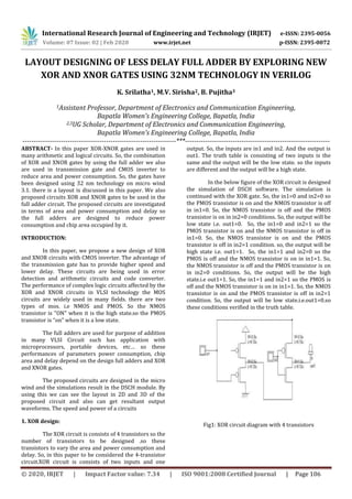
  • 1. International Research Journal of Engineering and Technology (IRJET) e-ISSN: 2395-0056 Volume: 07 Issue: 02 | Feb 2020 www.irjet.net p-ISSN: 2395-0072 © 2020, IRJET | Impact Factor value: 7.34 | ISO 9001:2008 Certified Journal | Page 106 LAYOUT DESIGNING OF LESS DELAY FULL ADDER BY EXPLORING NEW XOR AND XNOR GATES USING 32NM TECHNOLOGY IN VERILOG K. Srilatha1, M.V. Sirisha2, B. Pujitha3 1Assistant Professor, Department of Electronics and Communication Engineering, Bapatla Women's Engineering College, Bapatla, India 2,3UG Scholar, Department of Electronics and Communication Engineering, Bapatla Women's Engineering College, Bapatla, India --------------------------------------------------------------------***---------------------------------------------------------------- ABSTRACT- In this paper XOR-XNOR gates are used in many arithmetic and logical circuits. So, the combination of XOR and XNOR gates by using the full adder we also are used in transmission gate and CMOS inverter to reduce area and power consumption. So, the gates have been designed using 32 nm technology on micro wind 3.1. there is a layout is discussed in this paper. We also proposed circuits XOR and XNOR gates to be used in the full adder circuit. The proposed circuits are investigated in terms of area and power consumption and delay so the full adders are designed to reduce power consumption and chip area occupied by it. INTRODUCTION: In this paper, we propose a new design of XOR and XNOR circuits with CMOS inverter. The advantage of the transmission gate has to provide higher speed and lower delay. These circuits are being used in error detection and arithmetic circuits and code converter. The performance of complex logic circuits affected by the XOR and XNOR circuits in VLSI technology the MOS circuits are widely used in many fields. there are two types of mos. i.e NMOS and PMOS. So the NMOS transistor is "ON" when it is the high state.so the PMOS transistor is “on” when it is a low state. The full adders are used for purpose of addition in many VLSI Circuit such has application with microprocessors, portable devices, etc… so these performances of parameters power consumption, chip area and delay depend on the design full adders and XOR and XNOR gates. The proposed circuits are designed in the micro wind and the simulations result in the DSCH module. By using this we can see the layout in 2D and 3D of the proposed circuit and also can get resultant output waveforms. The speed and power of a circuits 1. XOR design: The XOR circuit is consists of 4 transistors so the number of transistors to be designed .so these transistors to vary the area and power consumption and delay. So, in this paper to be considered the 4-transistor circuit.XOR circuit is consists of two inputs and one output. So, the inputs are in1 and in2. And the output is out1. The truth table is consisting of two inputs is the same and the output will be the low state. so the inputs are different and the output will be a high state. In the below figure of the XOR circuit is designed the simulation of DSCH software. The simulation is continued with the XOR gate. So, the in1=0 and in2=0 so the PMOS transistor is on and the NMOS transistor is off in in1=0. So, the NMOS transistor is off and the PMOS transistor is on in in2=0 conditions. So, the output will be low state i.e. out1=0. So, the in1=0 and in2=1 so the PMOS transistor is on and the NMOS transistor is off in in1=0. So, the NMOS transistor is on and the PMOS transistor is off in in2=1 condition. so, the output will be high state i.e. out1=1. So, the in1=1 and in2=0 so the PMOS is off and the NMOS transistor is on in in1=1. So, the NMOS transistor is off and the PMOS transistor is on in in2=0 conditions. So, the output will be the high state.i.e out1=1. So, the in1=1 and in2=1 so the PMOS is off and the NMOS transistor is on in in1=1. So, the NMOS transistor is on and the PMOS transistor is off in in2=1 condition. So, the output will be low state.i.e.out1=0.so these conditions verified in the truth table. Fig1: XOR circuit diagram with 4 transistors
  • 2. International Research Journal of Engineering and Technology (IRJET) e-ISSN: 2395-0056 Volume: 07 Issue: 02 | Feb 2020 www.irjet.net p-ISSN: 2395-0072 © 2020, IRJET | Impact Factor value: 7.34 | ISO 9001:2008 Certified Journal | Page 107 Fig2: DSCH waveform of XOR circuit The DSCH timing diagrams to represent the CMOS full swing circuits. It consists of PMOS and NMOS so the timing diagram represents the delay and power. The above timing diagram to be represented in the XOR gate truth table. 3. XNOR design: XNOR gate is consists of 3 transistors so the many numbers of transistors to be Very delayed and power and area. So, the XNOR circuit is consists of two inputs and one output. So, the inputs are in1 and in2. And the output is out1.XNOR truth table is consists of two inputs that are the same the output will be the high state. So, the inputs are different the output will be the low state. In this below figure XNOR gate circuit is the simulation of DSCH software. The simulation is continued with the XNOR gate. So, the inputs are in1=0 and in2=0 so the PMOS transistor is on and the NMOS transistor is off state in in1=0. Otherwise, the PMOS transistor is on and the NMOS transistor is off state in in2=0. So, the output will be high state i.e. out1=1. So, the inputs are in1=0 and in2=1.so the PMOS transistor is on and the NMOS transistor is off state in in1=0. Otherwise, the PMOS transistor is off and the NMOS transistor is on the state in in2=0. So, the output will be high state i.e. out1=1. So, the inputs are in1=1 and in2=0.so the PMOS transistor is off and the NMOS transistor is on the state in in1=1. Otherwise, the PMOS transistor is off and the NMOS transistor is on the state in in2=0. So, the output will be low state i.e. out1=0. So, the inputs are in1=1 and in2=1.so the PMOS transistor is off and the NMOS transistor is on the state in in1=1. Otherwise, the PMOS transistor is off and the NMOS transistor is on the state in in2=1. So, the output will be high state i.e. out1=1.so these conditions are verified in the truth table. In the below fig4 the DSCH timing diagrams to represent the CMOS full swing circuits. It consists of PMOS and NMOS so the timing diagram represents the delay and power. The above timing diagram to be represented in the XOR gate truth table. Fig3: XNOR circuit diagram Fig4: DSCH timing diagram of XNOR circuit 4. Full adder design: The full adder design is to be consists of XOR and XNOR gates so it is consists of new XOR and XNOR gates to be implemented in full adder circuit. The full adder circuit consists of three inputs and two outputs .so the inputs are in1,in2,in3, and the outputs are the sum and carry.i.e out1 and out2. Full adder circuits to be designed in DSCH software. In the below figure full adder circuit is consists of 8 transistors. So it is a minimum number of transistors to b used. It is finding the area and delay and power consumption of circuits. So these conditions to be verified in the truth table. So the simulation occurs in the DSCH software. In full adder circuit is proposed with DSCH software. So the inputs are in1=0 and in2=0 and in3=0 the operation is included is p1 is on and n1 is off and n2 is on so the p2 is on and n2 off state. And the n3 is
  • 3. International Research Journal of Engineering and Technology (IRJET) e-ISSN: 2395-0056 Volume: 07 Issue: 02 | Feb 2020 www.irjet.net p-ISSN: 2395-0072 © 2020, IRJET | Impact Factor value: 7.34 | ISO 9001:2008 Certified Journal | Page 108 on state and n4 is off state. So the p3 on state and n5 off state. So the out1 will be a low state. I.e. sum=0 and the out2 will be low state.i.e carry =0.otherwise these conditions to be verified in that of the truth table. So the inputs are in1=0 and in2=0 and in3=1 the operation is included is p1 is on and n1 is off and n2 is on so the p2 is on and n2 off state. And the n3 is on state and n4 is off state. So the p3 on state and n5 off state. So the out1 will be a high state. I.e. sum=1 and the out2 will be low state.i.e carry =0. So the inputs are in1=0 and in2=1and in3=0 the operation is included is p1 is on and n1 is off and n2 is on so the p2 is on and n2 off state. And the n3 is on state and n4 is off state. So the p3 on state and n5 off state. So the output Will be the high state. I.e. sum=1 and the out2 will be the low state. I.e. carry=0 Fig5: Full adder circuit diagram Fig6: DSCH waveform of full adder Circuit 5. SIMULATION ANALYSIS 5.1 simulation of XOR circuit: Fig7: simulation of XOR layout The layout simulation occurs in micro wind 3.1 on the voltage range is 0.6v to 1.2v in 32nm technology. The simulation results of the XOR gate layout is consist of diffusion and n diffusion and contact cuts and metals and NMOS and PMOS transistors are used. The layout consists of the XOR circuit is due to the time and delay and power consumption. The time is very less is compared to the XOR gate. So minimum number transistors due to increase and time are high .layout designing in 32nm technology in 6metals and 1NMOS and 3PMOSes are used. So the simulation occurred due to the MOS characteristics. Fig8: characteristics of the layout The characteristics of layout due to the current and voltage. So the voltage occurs due to 35% and the current is due to 75%. So the current is increased and the voltage is decreased. So the simulation of layout time is 5ns and the delay is 1.3ms. so the delay is low and compared to that of the XNOR gate. The analog simulation id due to the Ids and VDS. So the power consumption is due to width to length.
  • 4. International Research Journal of Engineering and Technology (IRJET) e-ISSN: 2395-0056 Volume: 07 Issue: 02 | Feb 2020 www.irjet.net p-ISSN: 2395-0072 © 2020, IRJET | Impact Factor value: 7.34 | ISO 9001:2008 Certified Journal | Page 109 Fig9: analog simulation of XOR circuit 5.2 simulation of the XNOR circuit: Fig10: layout simulation of XNOR circuit The layout design of XNOR circuit I due to the micro wind 3.1 of the voltage range is 0.6v to 1.2v by using the 32nm technology. The layout simulation of the XNOR circuit is due to the p diffusion and p diffusion and metal and contact cuts. the simulation of the voltage range is due to 0.6v to 1.2v using 32nm CMOS delay is 823ns so the time is compared to that of high is XOR circuit. The layout simulation is due to voltages and currents and characteristics. So the 2NMOS and 1PMOS of being used for layout simulations. Fig11: characteristics of the layout The characteristics of the layout are due to current and voltages so the drain-source current ids and drain to source voltage VDS is t be considered. So the characteristics due to the current are the same constant and the voltage is varied to the difference. So the current is due to 75% and the voltage is due to the 45%. So the simulation of time is 5ns it is compared to that of the XOR gate is the same. So the delay is due to the low. Fig12: analog simulation of XNOR gate So the analog simulation of the XNOR gate is due t the current and voltages so the simulation is occurring the current to voltage and voltage to current and voltage to voltage characteristics. so the is simulated in 45nm technology. 5.3 simulation of full adder circuit Fig13: layout simulation of full adder diagram The layout simulation of the full adder circuit is designed in XOR and XNOR circuits. So the layout is simulated by using the micro wind 3.1 in the voltage range is 0.6v to 1.2 v using the 32nm CMOS technology. So the consists of power and delay of the full adder layout are 20ns and delay is 505s so it is the minimum number of transistors to be increased to the low delay and time is high.
  • 5. International Research Journal of Engineering and Technology (IRJET) e-ISSN: 2395-0056 Volume: 07 Issue: 02 | Feb 2020 www.irjet.net p-ISSN: 2395-0072 © 2020, IRJET | Impact Factor value: 7.34 | ISO 9001:2008 Certified Journal | Page 110 Fig14: characteristics of full adder circuit The characteristics of full adder simulation are due to the drain to source current and drain to source voltage. So the vary the IDS and VDS. So the IDS are due to increase and VDS is decreased. Fig15: analog simulation of the full adder circuit. The analog simulation of full adder circuit id due to the current and the voltage. So it is compared to that of delay is less compared to that of high XNOR and XNOR circuits. So the time is very high compared to that of XOR and XNOR circuits. so the voltage is increases and current is due to decreases. Fig16:3d view of full adder circuit The 3d view of the full adder circuit is due to all process is completed. RESULTS: The comparison of the circuits is XOR and XNOR gates by exploring are due to the full adder circuit in microwind3.1 by using 32nm technology. So the time and delay and number of transistors to be included. Table1: comparison between the XOR and XNOR and full adder circuits Parameter XOR XNOR Full adder Time 5ns 5ns 20ns delay 1.3ms 8.2ms 5.0ms no of transistors 4 3 8 TIME Fig17: Time graph The time graph to be represented in the XOR and XNOR gates due to the same time and these gates are explored by the full adder. So the time is very high in CMOS circuits. So the time graph to represent the time is increased and due to delay id increased. So the power is due to the high and compared to that of the full adder circuit. NO OF TRANSISTORS Fig18: number of transistors graph In the above graph to be represented In the XOR gate consists of 4 transistors and the XNOR gate consists of 3 0 10 20 30 xor xnor full adder xor Column1 Column2 0 1 2 3 4 5 xor xnor full adder Series 1 Series 2 Series 3
  • 6. International Research Journal of Engineering and Technology (IRJET) e-ISSN: 2395-0056 Volume: 07 Issue: 02 | Feb 2020 www.irjet.net p-ISSN: 2395-0072 © 2020, IRJET | Impact Factor value: 7.34 | ISO 9001:2008 Certified Journal | Page 111 transistors and it is due to the XNOR and XOR proposed with the full adder circuit with 8 transistors. CONCLUSION: In this paper, we proposed a new design of XOR and XNOR gates explored by using a full adder circuit. The performance of this circuit is compared to that of power and time and delay. So the simulation results are based on the 32 nm technology n microwind3.1 the proposed design circuits are less time and high delay. The simulation results id based on good driving ability with a good output signal and better performance. The proposed circuit is suitable for the low delay of circuits and the minimum number of transistors. REFERENCES: [1] W.Jyh-Ming, F.Sung -Chuan, and F. Wu -Shiung, "new efficient designs for XOR and XNOR functions on the transistor level, "solid-state circuits, IEEE Journal of, vol. 29, pp. 780-786, 1994. [2] K.E. Neil H.E. Weste, "principles of CMOS VLSI Design: A systems perspective, "1993. [3] Shamima Khatoon. “A novel design for highly compact low power area-efficient of 1-bit full adders ", international journal of advances in engineering & technology, 2012. [4] Manoj Kumar, Sandeep k. Arya, Sujatha Pandey. single-bit full adder design using 8 transistors with novel 3 transistors XOR gate, international journal of VLSI design &communication systems VLSICS. 2011;2(4).