amplifier teransistor
•Download as PPT, PDF•
0 likes•51 views

amplifier teransistor

Recommended
Recommended
More Related Content
What's hot
What's hot (20)
Similar to amplifier teransistor
Similar to amplifier teransistor (20)
More from Rai Saheb Bhanwar Singh College Nasrullaganj
Recently uploaded
Recently uploaded (20)
amplifier teransistor
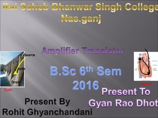
- 2. Gain medium Incoherent Light Coherent Light ECE 663 Source Drain Gate Valve ArteryVein Emitter Collector Base Ion Channel Dam Laser Heart Axonal conductionMOSFETBJT
- 3. • Output current can toggle between large and small (Switching Digital logic; create 0s and 1s) • Small change in ‘valve’ (3rd terminal) creates Large change in output between 1st and 2nd terminal (Amplification Analog applications; Turn 0.5 50)
- 4. Gain = 300
- 6. • How can we get ‘Gain’? • What is the structure of the device to get gain? • What is the equation for gain? • How can we use this equation to maximize gain? • How can we model this device as a circuit element? • What are its AC characteristics and speed?
- 7. P N W Vappl > 0 -+ N P W Vappl < 0 -+ Forward bias, + on P, - on N (Shrink W, Vbi) Allow holes to jump over barrier into N region as minority carriers Reverse bias, + on N, - on P (Expand W, Vbi) Remove holes and electrons away from depletion region I V I V
- 8. P N W Vappl > 0 -+ N P W Vappl < 0 -+ Holes from P region (“Emitter”) of 1st PN junction driven by FB of 1st PN junction into central N region (“Base”) Driven by RB of 2nd PN junction from Base into P region of 2nd junction (“Collector”) • 1st region FB, 2nd RB • If we want to worry about holes alone, need P+ on 1st region • For holes to be removed by collector, base region must be thin
- 9. + - + - IE IB IC IE = IB + IC ………(KCL) VEC = VEB + VBC ……… (KVL)
- 11. + - + - IE IB IC ECE 663 VEB, VBC > 0 VEC >> 0 IE, IC > 0 IB > 0 VEB >-VBC > 0 VEC > 0 but small IE > -IC > 0 IB > 0 VEB < 0, VBC > 0 VEC > 0 IE < 0, IC > 0 IB > 0 but small
- 12. ECE 663 Bias Mode E-B Junction C-B Junction Saturation Forward Forward Active Forward Reverse Inverted Reverse Forward Cutoff Reverse Reverse
- 13. ECE 663
- 14. ECE 663 PNP BJT Electrostatics
- 15. ECE 663 PNP BJT Electrostatics
- 16. ECE 663
- 17. ECE 663 Most holes diffuse to collector Large injection of Holes Collector Fields drive holes far away where they can’t return thermionically Few recombine in the base VEB > 0 VCB > 0
- 18. ECE 663