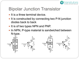
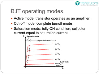
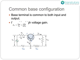
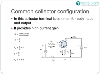
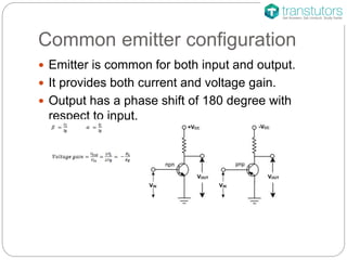
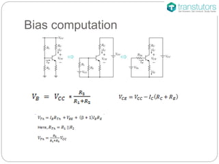
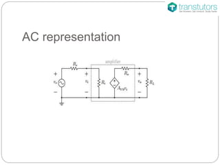
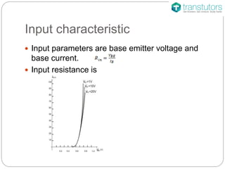
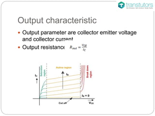
Common Emitter Configuration
Bipolar Junction Transistor
 It is a three terminal device.
 It is constructed by connecting two P-N junction
diodes back to back
 It is of two types NPN and PNP.
 In NPN, P-type material is sandwiched between
N-type.
BJT operating modes
 Active mode: transistor operates as an amplifier
 Cut-off mode: complete turnoff mode
 Saturation mode: fully ON condition; collector
current equal to saturation current
Common base configuration
 Base terminal is common to both input and
output.
 It provides high voltage gain.
Common collector configuration
 In this collector terminal is common for both input
and output.
 It provides high current gain.
Common emitter configuration
 Emitter is common for both input and output.
 It provides both current and voltage gain.
 Output has a phase shift of 180 degree with
respect to input.
Bias computation
AC representation
Input characteristic
 Input parameters are base emitter voltage and
base current.
 Input resistance is
Output characteristic
 Output parameter are collector emitter voltage
and collector current.
 Output resistance is
Hey Friend,
This was just a summary on Common Emitter Configuration. For
more detailed information on this topic, please type the link given
below or copy it from the description of this PPT and open it in a
new browser window.www.transtutors.com/homework-help/electrical-
engineering/transistors/common-emitter-configuration.aspx

Common Emitter Configuration | Electronical Engineering

  • 1.
  • 2.
    Bipolar Junction Transistor It is a three terminal device.  It is constructed by connecting two P-N junction diodes back to back  It is of two types NPN and PNP.  In NPN, P-type material is sandwiched between N-type.
  • 3.
    BJT operating modes Active mode: transistor operates as an amplifier  Cut-off mode: complete turnoff mode  Saturation mode: fully ON condition; collector current equal to saturation current
  • 4.
    Common base configuration Base terminal is common to both input and output.  It provides high voltage gain.
  • 5.
    Common collector configuration In this collector terminal is common for both input and output.  It provides high current gain.
  • 6.
    Common emitter configuration Emitter is common for both input and output.  It provides both current and voltage gain.  Output has a phase shift of 180 degree with respect to input.
  • 7.
  • 8.
  • 9.
    Input characteristic  Inputparameters are base emitter voltage and base current.  Input resistance is
  • 10.
    Output characteristic  Outputparameter are collector emitter voltage and collector current.  Output resistance is
  • 11.
    Hey Friend, This wasjust a summary on Common Emitter Configuration. For more detailed information on this topic, please type the link given below or copy it from the description of this PPT and open it in a new browser window.www.transtutors.com/homework-help/electrical- engineering/transistors/common-emitter-configuration.aspx