
Recommended
More Related Content
Similar to 8255.ppt
Similar to 8255.ppt (20)
Recently uploaded
Recently uploaded (20)
8255.ppt
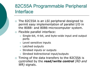
- 1. 82C55A Programmable Peripheral Interface The 82C55A is an LSI peripheral designed to permit easy implementation of parallel I/O in the 8088- and 8086-microcomputer system. Flexible parallel interface: Single-bit, 4-bit, and byte-wide input and output ports Level sensitive inputs Latched outputs Strobed inputs or outputs Strobed bidirectional input/outputs Timing of the data transfers to the 82C55A is controlled by the read/write control (RD and WR) signals.
- 2. 8255 -PPI Programmable Peripheral Interface
- 3. 8255 –PPI Modes of Operation Programmable Peripheral Interface Modes BSR BIT SET-REST I/O MODE MODE 0 Basic I/O Mode MODE 1 Strobed I/O Mode MODE 2 Strobed Bidirectional I/O
- 4. 82C55A Programmable Peripheral Interface (cont.) Block diagram of the 82C55A
- 5. 82C55A Programmable Peripheral Interface (cont.) The source or destination register within the 82C55A is selected by a 2-bit register select code (A1A0). The chip-select (CS) input must be logic 0 during all read or write operations to the 82C55A. The reset (RESET) is used to initialize the 82C55A. Three byte-wide ports (port A, port B, port C) can be configured for input or output operation. This gives us a total of 24 I/O lines. The 82C55A contains an 8-bit internal control register for software control. A write bus cycle to the 82C55A with register-select code A1A0 = 11, and an appropriate control word is used to modify the control register.
- 6. Cycles A1 A2 Register 0 0 Port A 0 1 PORT B 1 0 PORT C 1 1 CWR RD’ WR’ CS’ Unselect x x 1 READ 0 1 0 WRITE 1 0 0
- 7. Output (Write) Cycle RD’ WR’ CS’ A1 A2 Input Read Cycle 1 0 0 0 0 Data Bus To Port A 1 0 0 0 1 Data Bus To Port B 1 0 0 1 0 Data Bus To Port C 1 0 0 1 1 Data Bus to CWR
- 8. 82C55A Programmable Peripheral Interface (cont.) Addressing an 82C55A using the microcomputer interface signals
- 9. 82C55A Programmable Peripheral Interface (cont.) EXAMPLE: What is the addresses of port A, port B, port C of the 82C55A device? Solution: To access port A, A1A0 = 00, A15 = A14 = 1, A13 = A12 = … = A2 = 0, which gives the port A address as 1100 0000 0000 00002 = C00016 Similarly, it can be determined that the address of port B equals C00116, that of port C is C00216, and the address of the control register is C00316.
- 10. 8255 MODE INSTRUCTION FORMAT PORT C (UPPER) 1- Input 0- Output PORT A 1- Input 0- Output Mode select 0 0 - Mode 0 01 – Mode 1 1X – Mode 2 Mode set 1 – Active PORT B 1- Input 0- Output PORT C LOWER) 1- Input 0- Output Mode select 0 - Mode 0 1 – Mode 1
- 11. BSR Mode D3 D2 D1 Selected Bits of PORT C 0 0 0 C0 0 0 1 C1 0 1 0 C2 0 1 1 C3 1 0 0 C4 1 0 1 C5 1 1 0 C6 1 1 1 C7
- 12. 82C55A Programmable Peripheral Interface (cont.) Mode 0 – Simple I/O operation Mode 0 port pin functions
- 13. 82C55A Programmable Peripheral Interface (cont.) Mode 0 control words and corresponding input/output configurations
- 14. 82C55A Programmable Peripheral Interface (cont.)
- 15. 82C55A Programmable Peripheral Interface (cont.)
- 16. 82C55A Programmable Peripheral Interface (cont.)
- 17. 82C55A Programmable Peripheral Interface (cont.) EXAMPLE: What is the mode and I/O configuration for ports A, B, and C of an 82C55A after its control register is loaded with 8216? Solution: Expressing the control register contents in binary form, we get D7D6D5D4D3D2D1D0 = 100000102 Since D7 is 1, the modes of operation of the ports are selected by the control word. D0 = 0 Lower four bits of port C are outputs. D1 = 1 Port B is an input port. D2 = 0 Mode 0 for both port B and the lower four bits of port C.
- 18. 82C55A Programmable Peripheral Interface (cont.) The next for bits configure the upper part of port C and port A: D3 = 0 Upper four bits of port C are outputs. D4 = 0 Port A is an output port. D6D5 = 00 Mode 0 for both port A and the upper four bits of port C
- 19. 82C55A Programmable Peripheral Interface (cont.) Mode 1 – Strobed I/O In mode 1, the A and B ports are configured as two independent byte-wide I/O ports, each of which has a 4-bit control/data port associated with it. The control/data ports are formed from the lower and upper nibbles of port C, respectively In mode 1, data applied to an input port must be strobed in with a signal produced in external hardware An output port in mode 1 is provided with handshake signals that indicate when new data are available at its outputs and when an external device has read these values
- 20. 82C55A Programmable Peripheral Interface (cont.) Mode 1 – Strobed I/O Mode 1 port pin functions
- 21. 82C55A Programmable Peripheral Interface (cont.) Mode 1 – Strobed I/O Mode 1, port A output and input configuration
- 22. 82C55A Programmable Peripheral Interface (cont.) Mode 1, port A input and output timing diagram
- 23. 82C55A Programmable Peripheral Interface (cont.) EXAMPLE: The following figures show how port B can be configured for mode 1 operation. Describe what happens in the left figure when the STBB input is pulsed to logic 0. Assume that INTEB is already set to 1.
- 24. 82C55A Programmable Peripheral Interface (cont.) SOLUTION: As STBB is pulsed, the byte of data at PB7 through PB0 is latched into the port B register. This causes the IBFB output to switch to 1. Since INTEB is 1, INTRB switches to logic 1.
- 25. 82C55A Programmable Peripheral Interface (cont.) Mode 2 – Strobed bidirectional I/O Mode 2 port pin functions
- 26. 82C55A Programmable Peripheral Interface (cont.) Mode 2 – Strobed bidirectional I/O Mode 2 input/output configuration
- 27. 82C55A Programmable Peripheral Interface (cont.) Mode 2 – Strobed bidirectional I/O Mode 2 bit set/reset format
- 28. 82C55A Programmable Peripheral Interface (cont.) EXAMPLE The interrupt-control flag INTEA for output port A in mode 1 is controlled by PC6. Using the set/reset feature of the 82C55A, what command code must be written to the control register of the 82C55A to set it to enable the control flag? Solution: To use the set/reset feature, D7 must be logic 0. Moreover, INTEA is to be set; therefore, D0 must be logic 1. Finally, to select PC6, the code at bits D3D2D1 must be 110. The rest of the bits are don’t-care states. This gives us the control word D7D6D5D4D3D2D1D0 = 0XXX11012 Replacing the don’t-care states with the 0 logic level, we get D7D6D5D4D3D2D1D0 = 000011012 = 0D16
- 29. 82C55A Programmable Peripheral Interface Mixed modes Combined mode 2 and mode 0 (input) control word and I/O configuration
- 30. 82C55A Programmable Peripheral Interface EXAMPLE: What control word must be written into the control register of the 82C55A such that port A is configured for bidirectional operation and port B is set up with mode 1 outputs? Solution: To configure the operating mode of the ports of the 82C55A, D7 must be 1. Port A is set up for bidirectional operation by making D6 logic 1. In this case, D5 through D3 are don’t-care states: D5D4D3 = XXX2 Mode 1 is selected for port B by logic 1 in D2 and output operation by logic 0 in D1. D0 is a don’t-care state D7D6D5D4D3D2D1D0 = 11XXX10X2 = 110001002 = C416
- 31. 82C55A Programmable Peripheral Interface Mixed modes Combined mode 2 and mode 1 (output) control word and I/O configuration
- 32. 82C55A Programmable Peripheral Interface EXAMPLE Write the sequence of instructions needed to load the control register of an 82C55A with the control word formed in the previous example. Assume that the control register of the 82C55A resides at address 0F16 of the I/O address space? Solution: First we must load AL with C416 . This is the value of the control word that is to be written to the control register at address 0F16. The move instruction used to load AL is MOV AL, 0C4H These data are output to the control register with OUT instruction OUT 0FH, AL Because the I/O address of the control register is less than FF16, this instruction uses direct I/O.
- 33. 82C55A Programmable Peripheral Interface When the 82C55A is configured in mode 1 or mode 2 operations, most of the pins of port C perform I/O control functions. Mode 1 status information for port C Mode 1 status information for port C
- 34. 82C55A Implementation of Parallel Input/Output Ports 82C55A parallel I/O ports in an 8088-based microcomputer
- 35. 82C55A Implementation of Parallel Input/Output Ports EXAMPLE: What must be the address bus inputs of the circuit in the previous figure if port C of PPI 14 is to be accessed? Solution: To enable PPI 14, the 74F138 must be enabled for operation and its O7 output switched to logic 0. This requires enable input G2B = 0 and chip select code CBA = 111. This in turn requires from the bus that A0 = 0 to enable 74F138 and A5A4A3 = 111 to select PPI 14 Port C of PPI 14 is selected with A1A0 = 10, which from the bus requires that A2A1 = 10 The rest of the address bits are don’t-care states: XXXXXXXXXX111100
- 36. 82C55A Implementation of Parallel Input/Output Ports EXAMPLE Assume that in the previous figure, PPI 14 is configured so that port A is an output port, both ports B and C are input ports, and all three ports are set up for mode 0 operation. Write a program that will input that data at port B and C, find the difference (port C) – (port B), and output this difference to port A. Solution: Port A address = 001110002 = 3816 Similarly, Port B address = 3A16, Port C address = 3C16 Therefore, IN AL, 3AH ; Read port B MOV BL, AL ; Save data from port B IN AL, 3CH ; Read port C SUB AL, BL ; Subtract B from C OUT 38H, AL ; Write to port A
- 37. 82C55A Implementation of Parallel Input/Output Ports 82C55A parallel I/O ports in an 8086-based microcomputer
- 38. Memory-Mapped Input/Output Ports The full 20-bit address is available for addressing I/O. Memory-mapped I/O devices can reside anywhere in the 1Mbyte memory address space of the 8088. During I/O operations, memory read and write bus cycles are initiated instead of I/O bus cycles. Memory instructions, not input/output instructions, are used to perform data transfer.
- 39. Memory-Mapped Input/Output Ports Memory-mapped 82C55A parallel I/O ports in an 8088- based microcomputer
- 40. Memory-Mapped Input/Output Ports EXAMPLE: Which I/O port in the previous figure is selected for operation when the memory address output on the bus is 0040216? Solution: We begin by converting the address to binary form. This gives A19…A1A0 = 000000000100000000102 In this address, bits A10 = 1 and A0 = 0. Therefore, the 74F138 address decoder is enabled whenever IO/M = 0. A5A4A3 = 000 This input code switches decoder output O0 to logic 0 and chip selects PPI 0 for operation. The address bits applied to the port select inputs of the PPI are A2A1 = 01. These inputs cause port B to be accessed. Thus, the address 0040216 selects port B on PPI 0 for memory-map I/O.
- 41. Memory-Mapped Input/Output Ports EXAMPLE: Write the sequence of instructions needed to initialize the control register of PPI 0 in the circuit of the previous figure so that port A is an output port, ports B and C are input ports, and all three ports are configured for mode 0 operation. Solution: The control byte required to provide this configuration is:
- 42. Memory-Mapped Input/Output Ports From the circuit diagram, the memory address of the control register for PPI 0 is found to be 000000000100000001102 = 0040616 Since PPI 0 is memory mapped, the following move instructions can be used to initialized the control register: MOV AX, 0 ; Create data segment at 00000H MOV DS, AX MOV AL, 8BH ; Load AL with control byte MOV [406H], AL ; Write control byte to PPI 0 control register
- 43. Memory-Mapped Input/Output Ports EXAMPLE: Assume that PPI 0 in the previous figure is configured as described in the previous example. Write a program that will input the contents of ports B and C, AND them together, and output the results to port A. Solution: The addresses of the three I/O ports on PPI 0 are: Port A = 0040016 Port B = 0040216 Port C = 0040416 Now we set up a data segment at 0000016 and the program is: AND AX, 0 ; Create data segment at 00000H MOV DS, AX MOV BL, [402H] ; Read port B MOV AL, [404H] ; Read port C AND AL, BL ; AND data at port B and C MOV [400H], AL ; Write to port A