1. Lecture-49
INTEL 8255: (Programmable Peripheral Interface)
In previous lectures we have discussed how to interface I/O
devices with the system bys. If an input device, for example 8-toggle
switches, are to be interfaced with the processor, they can be
connected to data bus through 8-bit tri-state bus buffer. The status of
switches can be read using IN PORT instruction in isolated I/O mode.
The buffer is enabled during the execution of 3rd
machine cycle
(IORDMC) when IO/M =1, RD =0 and address of the device is
available on address bus. Similarly, if an output device, for example
8-LEDs are to be interfaced, they can be connected to data bus using
8-bit latch. The 8-bit data can be sent to LEDs using OUT PORT
instruction in isolated I/O mode. During the 3rd
machine cycle
(IOWRMC), the latch is enabled when IO/M =1, WR =0 and address
of the output device is available on address bus.
If the system is designed using buffer and latches to interface
input and out devices, then in future, it is not possible to change any
input device with the output device or vice-versa. In order to make it
simpler, Intel has designed 8255A chip to interface I/O devices.
The Intel 8255A is a general purpose programmable I/O device
designed for use with Intel microprocessors. It consists of three 8-bit
bidirectional I/O ports (24 I/O lines) that can be configured to meet
different system I/O needs. The three ports are designated as PORT
A, PORT B and PORT C. Port A contains one 8-bit output latch/buffer
and one 8-bit input buffer. Port B is same as PORT A or PORT B.
However, PORT C is split into two parts- PORT C lower (PC3-PC0)
2. and PORT C upper (PC7-PC4) by the control word. The four ports –
two 8-bit PORTs and two 4-bit PORTs are divided in two groups
Group A (PORT A and upper PORT C) Group B (PORT B and lower
PORT C) for programming purpose. These two groups can be
programmed in three different modes:
1. Mode-0
2. Mode-1
3. Mode-2
In the first mode, mode-0, each group may be programmed in either
input mode or output mode (PORT A, PORT B, PORT C lower,
PORT C upper). In mode-1, the second mode, each group may be
programmed to have 8-lines of input or output (PORT A or PORT B)
and of the remaining 4-lines (PORT C lower or PORT C upper) 3-
lines are used for handshaking and interrupt control signals. The third
mode of operation, mode-2, is a bidirectional bus mode which uses 8-
lines (PORT A) only for a bidirectional bus and five lines (PORT C
upper 4 lines and borrowing one line from PORT C lower) for
handshaking and control signals. PORT A and PORT B have both
input and output buffers and latches but PORT C has output latch
and input buffer.
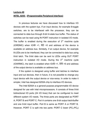
The 8255A is contained in a 40-pin package, whose pin out is
shown in fig.9.1.
3. Fig.9.1 Pin Configuration of Intel 8225 PPI
The block diagram is shown in fig.9.2.
Fig.9.2 Functional Block Diagram of Intel 82255 PPI
1
2
3
4
5
6
7
8
9
10
11
12
13
14
15
16
17
18
19
20
37
38
39
40
D7
D6
D5
D4
D3
D2
D1
D0
VCC
WRRD
CS
8255
GND
21
22
36
35
34
33
32
31
30
29
28
27
26
25
24
23
RESET
PA0
PA1
PA2
PA3
PA7
PA6
PA5
PA4
A1
A0
PC0
PC5
PC6
PC7
PC4
PC3
PC2
PC1
PB0
PB2
PB1
PB5
PB3
PB4
PB7
PB6
Data Bus
Buffer
Read/Write
Control
Logic
D7-D0
RD
WR
A0
CS
88
Group B
Control
A1
8
4
RESET
Group A
Control
PA7-PA0
8Group A
PORT A
PC7-PC4
4
Group A
PORT C Upper
8
4
PB7-PB0
8Group B
PORT B
PC3-PC0
4
Group B
PORT C Lower
PIN Names
RESET – Reset input
CS - Chip selected
RD - Read input
WR - Write input
A0 A1 – Port Address
PA7 – PA0 – PORT A
PB7 – PB0 – PORT B
PC7 – PC0 – PORT C
VCC - +5V
GND - Ground
4. Functional Description:
This support chip is a general purpose I/O component to interface
peripheral equipment to the microcomputer system bus. It is
programmed by the system software so that normally no external
logic is necessary to interface peripheral devices or structures.
Data Bus Buffer:
It is a tri-state 8-bit buffer used to interface the chip to the system
data bus. Data is transmitted or received by the buffer upon execution
of input or output instructions by the CPU. Control words and status
information are also transferred through the data bus buffer. The data
lines are connected to BDB of 𝜇p.
Read/Write and Logic Control:
The function of this block is to control the internal operation of the
device and to control the transfer of data and control or status words.
It accepts inputs from the CPU address and control buses and, in
turn, issues command to both the control groups.
CS (Chip Select):
A low on this input selects the chip and enables the communication
between 8255A & the CPU. It is connected to the output of address
decode circuitry to select the device when it is addressed.
RD (Read):
A low on this input enables the 8255A to send the data or status
information to the CPU on the data bus.
5. WR (Write):
A low on this input pin enables the CPU to write data or control words
into the 8255A.
A1, A0 Port Select:
These input signals, in conjunction with the RD and WR inputs,
control the selection of one of the three ports or the control word
registers. They are normally connected to the least significant bits of
the address bus (A0 and A1).
The basic operation of these control signals is given in the
following Table:
A1 A0 RD WR CS Input –Output operation
0 0 0 1 0 PORT A Data bus
0 1 0 1 0 PORT B Data bus
1 0 0 1 0 PORT C Data bus
0 0 1 0 0 Data bus PORT A
0 1 1 0 0 Data bus PORT B
1 0 1 0 0 Data bus PORT C
1 1 1 0 0 Data bus CWR
All other states put data bus into tri-state/illegal condition.
RESET:
A high on this input pin clears the control register and all ports (PORT
A, PORT B & PORT C) are initialized in input mode. This is
connected to RESET OUT of 8085A. This is done to prevent
destruction of circuitry connected to port lines. If port lines are
6. initialized as output after a power up or reset, the port might try to
output into the output of a device connected to same inputs might
destroy one or both of them.
To understand why the programmable ports are automatically
programmed in input mode just after power on or reset, let us
consider the port is programmed by default in output mode. The user
might have connected an output device (LEDs) or an input device
(toggle switches) to the port before switching on power as shown in
fig.9.3.
Fig.9.3 Ports Programmed as Output Port by Default
The port, if programmed in output mode, derives the output lines and
the data flows from the port to device. Whatever may be the default
data output, the LEDs will be switched on or off accordingly. If an
input device is connected to the same port (programmed in output
mode by default), then the output device (toggle switches) also drives
the data lines. The data lines will be driven from both the ends and,
therefore, there will be data bus contamination.
Now let us consider the port is programmed in input mode by
default and the user has connected either input device or an output
Port
Programmed
as Output
Output
Device
Direction of data flow
Port
Programmed
as Output
Input
Device
Data Bus Conflict as both Port
and Device Outputs the data
7. device to this port as shown in fig.9.4. If an input device is connected
to the port, the device drives the data lines and the port accepts the
data from these lines. The data flows from the device to the port.
However, if an output device is connected to this port (programmed
by default in input mode), both the device and the port can only
accept data from the data lines. In this case, no data flow takes place
but there will be no data bus contamination. After switch on, the port
will be programmed in desired mode. That is the reason why
programmable ports are programmed in input mode just after power
on or reset.
Fig.9.4 Ports Programmed as Input Port by Default
PORTs A, B and C:
The 8255A contains three 8-bit ports (A, B and C). All can be
configured in a variety of functional characteristic by the system
software.
PORT A:
One 8-bit data output latch/buffer and one 8-bit data input latch.
Port
Programmed
as Input
Output
Device
Direction of data flow
Port
Programmed
as Input
Input
Device
No Data Bus Conflict as both
Port and Device can accept the
data from the bus
8. PORT B:
One 8-bit data output latch/buffer and one 8-bit data input buffer.
PORT C:
One 8-bit data output latch/buffer and one 8-bit data input buffer (no
latch for input). This port can be divided into two 4-bit ports under the
mode control. Each 4-bit port contains a 4-bit latch and it can be used
for the control signal outputs and status signals inputs in conjunction
with ports A and B.
Group A & Group B control:
The functional configuration of each port is programmed by the
system software. The control words outputted by the CPU configure
the associated ports of the each of the two groups. Each control block
accepts command from Read/Write content logic receives control
words from the internal data bus and issues proper commands to its
associated ports.
Control Group A – Port A & Port C upper
Control Group B – Port B & Port C lower
The control word register can only be written into. No read operation
of the control word register is allowed.