SlideShare a Scribd company logo
1 of 74
Download to read offline
Delft
University
of
Technology
Code ET4351
Digital Design Flow
Tutorial for EDA Tools:
Synopsys Design Compiler
Mentor Modelsim
Cadence INNOVUS V20.4
Ir. A.C. de Graaf
Dr.ir. T.G.R.M. van Leuken
ASIC Design
Zagazig University
Preface
This document describes the top-down design flow of the implementation a SoC design. Starting from
an example HDL description the designer is guided through all the design steps to tapeout GDS2 layout
description.
This tutorial is derived from "Top-Down digital design flow" version 3.1 (November 2006) by Alain Va-
choux, Microelectronic Systems Lab EPFL, Lausanne, Switzerland.
i
Contents
1 Introduction 1
1.1 Top-down design flow . . . . . . . . . . . . . . . . . . . . . . . . . . . . . . . . . . . . 2
1.2 Design project organization . . . . . . . . . . . . . . . . . . . . . . . . . . . . . . . . . 3
1.3 VHDL example: FIR-Filter . . . . . . . . . . . . . . . . . . . . . . . . . . . . . . . . . 5
1.4 Design flow steps . . . . . . . . . . . . . . . . . . . . . . . . . . . . . . . . . . . . . . . 6
2 VHDL and Verilog simulation 8
2.1 Starting the Modelsim graphical environment . . . . . . . . . . . . . . . . . . . . . . . . 8
2.2 Simulation of (pre-synthesis) RTL VHDL models . . . . . . . . . . . . . . . . . . . . . . 9
2.3 Simulation of the post-synthesis Verilog model with timing data . . . . . . . . . . . . . . 12
2.4 Simulation of the post-route Verilog model with timing data . . . . . . . . . . . . . . . . 14
3 Logic synthesis 15
3.1 Loading and checking the design . . . . . . . . . . . . . . . . . . . . . . . . . . . . . . 15
3.2 Constraining the design . . . . . . . . . . . . . . . . . . . . . . . . . . . . . . . . . . . . 17
3.3 Mapping and Optimization . . . . . . . . . . . . . . . . . . . . . . . . . . . . . . . . . . 17
3.4 Generating reports . . . . . . . . . . . . . . . . . . . . . . . . . . . . . . . . . . . . . . 18
3.5 Check design and generate output . . . . . . . . . . . . . . . . . . . . . . . . . . . . . . 21
4 Standard cell placement and routing 22
4.1 Starting INNOVUS and importing the design . . . . . . . . . . . . . . . . . . . . . . . . 22
4.2 Design import . . . . . . . . . . . . . . . . . . . . . . . . . . . . . . . . . . . . . . . . . 22
4.3 Floorplan Specification . . . . . . . . . . . . . . . . . . . . . . . . . . . . . . . . . . . . 25
4.4 Power ring/stripe creation and routing . . . . . . . . . . . . . . . . . . . . . . . . . . . . 27
4.4.1 Define global net connections . . . . . . . . . . . . . . . . . . . . . . . . . . . . 27
4.4.2 Define power rings . . . . . . . . . . . . . . . . . . . . . . . . . . . . . . . . . . 28
4.4.3 Routing the power grid . . . . . . . . . . . . . . . . . . . . . . . . . . . . . . . . 29
4.5 Core cell placement . . . . . . . . . . . . . . . . . . . . . . . . . . . . . . . . . . . . . 30
4.6 Post-placement timing analysis . . . . . . . . . . . . . . . . . . . . . . . . . . . . . . . 31
4.7 Clock tree synthesis (optional) . . . . . . . . . . . . . . . . . . . . . . . . . . . . . . . . 32
4.8 Filler cell placement . . . . . . . . . . . . . . . . . . . . . . . . . . . . . . . . . . . . . 33
4.9 Design routing . . . . . . . . . . . . . . . . . . . . . . . . . . . . . . . . . . . . . . . . 34
4.10 Post-routing timing optimization and analysis . . . . . . . . . . . . . . . . . . . . . . . . 35
4.11 Design checks . . . . . . . . . . . . . . . . . . . . . . . . . . . . . . . . . . . . . . . . 36
4.12 Report generation . . . . . . . . . . . . . . . . . . . . . . . . . . . . . . . . . . . . . . . 37
4.13 Post-route timing data extraction . . . . . . . . . . . . . . . . . . . . . . . . . . . . . . . 39
4.14 Post-route netlist generation . . . . . . . . . . . . . . . . . . . . . . . . . . . . . . . . . 40
4.15 GDS2 file generation . . . . . . . . . . . . . . . . . . . . . . . . . . . . . . . . . . . . . 41
ii
CONTENTS iii
4.16 Using scripts . . . . . . . . . . . . . . . . . . . . . . . . . . . . . . . . . . . . . . . . . 41
A VHDL Netlists 42
A.1 File: filter.vhd . . . . . . . . . . . . . . . . . . . . . . . . . . . . . . . . . . . . . . . . . 42
A.2 File: filter_top.vhd . . . . . . . . . . . . . . . . . . . . . . . . . . . . . . . . . . . . . . 46
A.3 File: filter_soc.vhd . . . . . . . . . . . . . . . . . . . . . . . . . . . . . . . . . . . . . . 48
A.4 File: filter_soc_tb.vhd . . . . . . . . . . . . . . . . . . . . . . . . . . . . . . . . . . . . . 52
B Tool Scripts 55
B.1 Synopsys: Design Compiler . . . . . . . . . . . . . . . . . . . . . . . . . . . . . . . . . 55
B.1.1 setup.tcl . . . . . . . . . . . . . . . . . . . . . . . . . . . . . . . . . . . . . . . . 55
B.1.2 load_design.tcl . . . . . . . . . . . . . . . . . . . . . . . . . . . . . . . . . . . . 56
B.1.3 constraints.tcl . . . . . . . . . . . . . . . . . . . . . . . . . . . . . . . . . . . . . 58
B.1.4 compile.tcl . . . . . . . . . . . . . . . . . . . . . . . . . . . . . . . . . . . . . . 59
B.1.5 check_save.tcl . . . . . . . . . . . . . . . . . . . . . . . . . . . . . . . . . . . . 60
B.1.6 syn.tcl . . . . . . . . . . . . . . . . . . . . . . . . . . . . . . . . . . . . . . . . . 61
B.2 Cadence: INNOVUS . . . . . . . . . . . . . . . . . . . . . . . . . . . . . . . . . . . . . 61
B.2.1 setup.tcl . . . . . . . . . . . . . . . . . . . . . . . . . . . . . . . . . . . . . . . . 61
B.2.2 importDesign.tcl . . . . . . . . . . . . . . . . . . . . . . . . . . . . . . . . . . . 64
B.2.3 floorplan.tcl . . . . . . . . . . . . . . . . . . . . . . . . . . . . . . . . . . . . . . 64
B.2.4 powerplan.tcl . . . . . . . . . . . . . . . . . . . . . . . . . . . . . . . . . . . . . 64
B.2.5 placement.tcl . . . . . . . . . . . . . . . . . . . . . . . . . . . . . . . . . . . . . 66
B.2.6 cts.tcl . . . . . . . . . . . . . . . . . . . . . . . . . . . . . . . . . . . . . . . . . 66
B.2.7 route.tcl . . . . . . . . . . . . . . . . . . . . . . . . . . . . . . . . . . . . . . . . 66
B.2.8 verify.tcl . . . . . . . . . . . . . . . . . . . . . . . . . . . . . . . . . . . . . . . 67
B.2.9 results.tcl . . . . . . . . . . . . . . . . . . . . . . . . . . . . . . . . . . . . . . . 67
B.2.10 par.tcl . . . . . . . . . . . . . . . . . . . . . . . . . . . . . . . . . . . . . . . . . 68
Chapter 1
Introduction
This document details the typical steps of a top-down digital VHDL/Verilog design flow with the help of a
simple design example.
The following tools are considered in this document:
• Modelsim V10.1f or V10.7c and up, from Mentor Graphics.
• Design Compiler and Design Vision SYN_2016.12 or higher from Synopsys.
• INNOVUS_17.11.000 or higher from Cadence Design Systems.
The design kit used is from IMEC. The process is UMC L65_LL, a 65 nm 8-metal CMOS process.
Each of the next chapters in this document is addressing a specific set of tasks. Chapter 2 is about VHDL
and Verilog simulation, chapter 3 describes the logic synthesis and chapter 4 describes the place and route
steps.
All tools have a GUI interface to work interactively, additionally it is possible to use Tcl-scripts. These
scripts contain the sequence of individual commands necessary to produce the result of a particular design
step and make the designflow reproduceable.
Both chapter 3 and 4 start with a description of the interactive way step by step, followed by using a Tcl
script doing all the interactive steps in one single step.
Throughout this text, commands are displayed with a gray background and the mentioned single step com-
mands are additionally framed by a black box.
1
CHAPTER 1. INTRODUCTION 2
1.1 Top-down design flow
Figure 1.1: Top-down design flow
Figure 1.1 illustrates the top-down flow that includes the following steps:
VHDL RTL model creation
The goal here is to develop synthesizable VHDL models at the RTL level (RTL means Register-
Transfer Level). Such models usually define a clear separation between control parts (e.g. finite
state machines-FSM) and operative parts (e.g. arithmetic and logic units). Registers are used to store
small size data between clock cycles. RAM/ROM memories are used to store large amounts of data
or program code. Blocks such as FSMs, ALUs, registers are usually described as behavioral models
that do not imply any particular gate-level implementation. Tools used at this step can range from
simple text editors to dedicated graphical environments that generate VHDL code automatically.
RTL simulation
The VHDL RTL models are validated through simulation by means of a number of test-benches also
written in VHDL.
RTL synthesis
The synthesis process infers a possible gate-level realization of the input RTL description that meets
user-defined constraints such as area, timings or power consumption. The design constraints are de-
fined outside the VHDL models by means of tool-specific commands. The targeted logic gates belong
to a library that is provided by a foundry or an IP company as part of a so-called design kit. Typical
gate libraries include a few hundreds of combinational and sequential logic gates. Each logic function
CHAPTER 1. INTRODUCTION 3
is implemented in several gates to accommodate several fan-out capabilities or drive strengths. The
gate library is described in a tool-specific format that defines, for each gate, its function, its area, its
timing and power characteristics and its environmental constraints.
The synthesis step generates several outputs: a gate-level VHDL net-list, a Verilog gate-level net-list,
and a SDF description. The first netlist is typically used for post-synthesis simulation, while the
second netlist is better suited as input to the place&route step. The SDF description includes delay
information for simulation. Note that considered delays are at this step correct for the gates but only
estimated for the interconnections.
Post-synthesis gate-level simulation
The testbenches used for RTL model validation can be reused (with possibly some modifications to
use the VHDL gate-level netlists). The gate-level simulation makes use of VHDL models for the
logic gates that are provided in the design kit. These VHDL models follow the VITAL modeling
standard to ensure proper back-annotation of delays through the SDF files generated by the synthesis
or the place&route step.
Standard cell place and route
The place&route (P&R) step infers a geometric realization of the gate-level netlist so-called a layout.
The standard cell design style puts logic cells in rows of equal heights. As a consequence, all logic
gates in the library have the same height, but may have different widths. Each cell has a power rail at
its top and a ground rail at its bottom.
The interconnections between gates are today usually done over the cells since current processes
allow several metal layers (i.e. 8 metal layers for the IMEC L65_LL process). As a consequence, the
rows may be abutted and flipped so power and ground rails are shared between successive rows.
The P&R step generates several outputs: a geometric description (layout) in GDS2 format, a SDF
description and a Verilog gate-level netlist. The SDF description now includes interconnect delay.
The Verilog netlist may be different from the one read as input as the P&R step may make further
timing optimizations during placement, clock tree generation and routing (e.g. buffer insertion).
Post-layout gate-level simulation
The Verilog gate-level netlist can be simulated by using the existing VHDL testbenches and the more
accurate SDF data extracted from the layout.
System-level integration
The layout description is then integrated as a block in the designed system. This step is not covered
in this document.
1.2 Design project organization
First we have to setup a proper work environment. The toolscripts need the CSH shell as command shell
while the standard shell after login is the Bash shell. So first we take care that the CSH shell is our default
command shell by:
cp /opt/eds/DesignLab/bin/dot.bashrc ~/.bashrc
Logout and login again.
Continue to add the DesignLab script directory to our PATH by:
source /opt/eds/DesignLab/bin/dlab.csh
CHAPTER 1. INTRODUCTION 4
Given the number of EDA tools and files used in the flow, it is strongly recommended to organize the
working environment in a proper way. To that end, the create_eda_project script can be used to create a
directory structure in which design files will be stored.
The use of the script is as follows:
create_eda_project <project-name>
where <project-name> is the name of the top-level directory that will host all design files for the projects.
For example, to create the project directory called ’filter_umc65’ that will be used to do the tasks presented
in the rest of this document, execute the following command:
create_eda_project filter_umc65
cd filter_umc65
The filter_umc65 top-level directory hosts the configuration files for logic simulation (Modelsim), logic
synthesis (Synopsys DC) and standard cell place and route (Cadence SoC INNOVUS). As a consequence,
it is required that the tools are always started from that point.
Figure 1.2 shows the proposed directory structure and the role of each subdirectory. The actual use of the
subdirectories and files will be explained while going throughout the tutorial in this document.
project_name/..........................................................project directory home
modelsim.ini...................................................setup file for Modelsim tool
DOC...........................................................documentation (pdf, text, etc.)
HDL..............................................................VHDL/Verilog source files
GATE .................................................................. gate-level netlists
RTL....................................................................RTL descriptions
TBENCH......................................................................testbenches
IP...........................................................external blocks (e.g., memories)
LAY..................................................................full-custom layout files
LIB.........................................................................design libraries
MSIM..................................................Modelsim library (VHDL, Verilog)
SNPS...................................................Synopsys library (VHDL, Verilog)
PAR......................................................................place & route files
BIN...................................................................commands, scripts
CONF..................................................................configuration files
CTS.............................................................clock tree synthesis files
DB ........................................................................ database files
DEX................................................................design exchange files
LOG............................................................................log files
RPT..........................................................................report files
SDC.........................................................system design constraint files
TEC.....................................................................technology files
TIM.........................................................................timing files
SIM.........................................................................simulation files
BIN...................................................................commands, scripts
OUT.........................................................output files (e.g., waveforms)
SYN ......................................................................... synthesis files
BIN...................................................................commands, scripts
DB ........................................................................ database files
LOG............................................................................log files
RPT..........................................................................report files
SDC.........................................................system design constraint files
TIM.........................................................................timing files
Figure 1.2: Design project structure.
CHAPTER 1. INTRODUCTION 5
1.3 VHDL example: FIR-Filter
The FIR-Filter example will be used as the reference design throughout the topdown flow.
To install the VHDL model and its associated testbenches in the project directory, enter the following
command in the top-level project directory filter_umc65:
install_design filter_umc65
In order to use the EDA tools and IMEC design kit, a script file called edadk.csh with the necessary PATHs
to the tools exists in the directory from which the tools are launched (the top-level project directory).
Add these PATHs to your current environment by executing:
source edadk.csh
For information on the IMEC design kits, find the IMEC documentation in:
/opt/eds/DesignKits/IMEC-UMC65/_G-01-LOGIC_MIXED_MODE65N-LL_LOW_K_UMC-IP/doc.
Listing 1.1 shows the entity declaration of the VHDL model of a generic 128 tap FIR-Filter. You will
find the complete VHDL model including the testbench in Appendix A.1-3. We will call this model the
Core.
Listing 1.1: Entity declaration of a synthesisable 128 tap FIR-Filter.
library ieee;
use ieee.std_logic_1164.all;
use ieee.numeric_std.all;
entity filter_soc is
generic (
CWIDTH : integer := 16;
CAW : integer := 7;
DWIDTH : integer := 16;
DAW : integer := 7
);
port (
ClkxCI : in std_logic;
ResetxRBI : in std_logic;
DataInxDI : in std_logic_vector(DWIDTH -1 downto 0);
DataInReqxSI : in std_logic;
DataInAckxSO : out std_logic;
DataOutxDO : out std_logic_vector(DWIDTH -1 downto 0);
DataOutReqxSO : out std_logic;
DataOutAckxSI : in std_logic
);
end filter_soc;
CHAPTER 1. INTRODUCTION 6
Figure 1.3 shows the hierarchy of the filter design. The chiplevel entity named filter_soc consists of compo-
nents IO-padcells and the toplevel filter design filter_top. Filter top consists of instances of the components
coeff, dataRam and filter. The IO-padcells connect the port signals to the outside world.
Filter_top
Filter
DataRam
Coeff Rom
Filter_soc
Figure 1.3: Hierarchy of the FIR filter chip
Listing ?? shows the testbench for the RTL model (file filter_soc_tb.vhd). The testbench for the mapped
netlist (file filter_soc_mapped_tb.vhd) can also be used for simulation of both the placed and routed Verilog
netlist. The file filter_top.io defines the positions of the IO-padcells for place and route.
The file filter_soc_syn.tcl in directory SYN/BIN is a Tcl script that performs synthesis of the VHDL model
in batch mode. The file filter_top_par.tcl in directory PAR/BIN is a Tcl script that performs the placement
and routing of the synthesized Verilog netlist in batch mode.
1.4 Design flow steps
Here are the main steps of the top-down design flow with references to the sections in the document that
give more details.
Step 1) Pre-synthesis VHDL simulation (tool: Modelsim)
2.1 Compilation of the RTL VHDL model and related testbench [2.2]
2.2 Simulation of the RTL VHDL model
Step 2) Logic synthesis (tool: Synopsys Design Compiler)
3.1 RTL VHDL model analysis
3.2 Design elaboration (generic synthesis)
3.3 Design environment definition (operating conditions, wire load model)
3.4 Design constraint definitions (area, clock, timings) [3.2]
CHAPTER 1. INTRODUCTION 7
3.5 Design mapping and optimization (mapping to gates) [3.3]
3.6 Report generation [3.4]
3.7 VHDL gate-level netlist generation [3.5]
3.8 Post-synthesis timing data (SDF) generation for the VHDL netlist [3.5]
3.9 Verilog gate-level netlist generation [3.5]
3.10 Design constraints generation for placement and routing [3.5]
Step 3) Post-synthesis VHDL simulation (tool: Modelsim) [2.3]
4.1 Compilation of the VHDL/Verilog netlist and related testbench
4.2 Simulation of the post-synthesis gate-level netlist with timing data
Step 4) Placement and routing (tool: Cadence INNOVUS)
5.1 Design import (technological data + Verilog netlist) [4.2]
5.2 Floorplan specification [4.3]
5.3 Power ring/stripe creation and routing [4.4]
5.4 Global net connections definition [4.4.1]
5.5 Core cell placement [4.5]
5.6 Post-placement timing analysis [4.6]
5.7 Clock tree synthesis (optional) [4.7]
5.8 Design routing [4.9]
5.9 Post-route timing optimization and analysis [4.10]
5.10 Filler cell placement [4.8]
5.11 Design checks [4.11]
5.12 Report generation [4.12]
5.13 Post-route timing data extraction [4.13]
5.14 Post-route netlist generation [4.14]
5.15 GDS2 file generation [4.15]
Step 5) Post-layout VHDL/Verilog simulation (tool: Modelsim) [2.4]
6.1 Compilation of the Verilog netlist and related testbench
6.2 Simulation of the post-synthesis or post-P&R gate-level netlist with PaR timing data
Chapter 2
VHDL and Verilog simulation
This chapter presents the main steps to perform the logic simulation of VHDL and Verilog models with the
Modelsim tool.
2.1 Starting the Modelsim graphical environment
To start the Modelsim environment, create first a work library in de directory LIB/MSIM then enter in the
vsim command in the Unix shell:
vlib LIB/MSIM/work
vmap work LIB/MSIM/work/
vsim -voptargs=+acc &
Figure 2.1: Modelsim console window
8
CHAPTER 2. VHDL AND VERILOG SIMULATION 9
The modelsim.ini file actually defines the mapping between logical design libraries and their physical
locations. Note that the Help menu on the top right allows one to access the complete documentation of
the tool. After having started the vsim GUI you have to compile all the VHDL source of your design into
the simulation library work. Now you have two options to simulate your model, either interactively or by
executing the following convenience scripts (see directory SIM/BIN) on the VSIM command line:
wave.do To start a wave window with the ports of the top level module.
start_msim[_mapped | _routed ].do To start up the simulation of the particular module.
run_msim[_mapped | _routed ].do To load the filter coefficients into the coefficient ROM and runs the
simulation for 300 us.
2.2 Simulation of (pre-synthesis) RTL VHDL models
The task here is to validate the functionality of the VHDL model that will be synthesized. The first step is
to compile the VHDL model and its associated testbench. There are two ways to compile VHDL models.
One way is to execute the vcom command from the command line of the Modelsim window:
ModelSim> vlog -quiet HDL/RTL/SYKA65_128X16X1CM2.v
ModelSim> vlog -quiet HDL/RTL/SPKA65_512X16BM1A.v
ModelSim> vcom -quiet HDL/RTL/coeffFAR.vhd
ModelSim> vcom -quiet HDL/RTL/dataRamFAR.vhd
ModelSim> vcom -quiet HDL/RTL/filter.vhd
ModelSim> vcom -quiet HDL/RTL/filter_top.vhd
ModelSim> vcom -quiet HDL/RTL/filter_soc.vhd
ModelSim> vcom -quiet -suppress 1288,1074,1194 HDL/TBENCH/filter_soc_tb.vhd
or alternatively execute the shell script compile_msim.sh from the CSH command line:
sh compile_msim.sh
The second way is to left-click on the Compile icon , to select the files to compile in the HDL/RTL
and HDL/TBENCH directories, click on Compile
and finally close the window (click Done). The
compiled modules are stored in the logical library
WORK which is mapped to the physical location
LIB/MSIM/work. Once VHDL (or Verilog) mod-
els have been successfully compiled in the design
library, it is possible to create a make file that can
be used to recompile only the required files. The
vmake command can only be run from a Unix shell
and creates the make file:
vmake > Makefile
The created file Makefile now defines the design unit dependencies and the compilation commands to
recompile only those source files that have been modified or that depend on modified files. To rebuild the
library, run the make command in the Unix shell
To simulate the RTL model, select the main menu item
1. Select the main menu item Simulate ⇒ Start simulation... to get the simulation dialog window.
2. Select from library work the architecture of the testbench and a resolution of 1ns.
CHAPTER 2. VHDL AND VERILOG SIMULATION 10
3. Click the Libraries tab to add the gate library umc65_generic_core
4. Unselect Énable optimization´
(off) .
5. Then click OK.
The main window now changes a bit to show the simulation hierarchy, the list of signals in the testbench
and the simulation console (with now the VSIM number> prompt).
Left clicking twice on an instance in the simulation hierarchy pane displays the corresponding VHDL source
in the right pane.
CHAPTER 2. VHDL AND VERILOG SIMULATION 11
The next step is to select the signals to display in simulation.
Right click in the Objects (top center) pane, then select
Add to Wave ⇒ Signals in Region.
Note that the appropriate hierarchy level is selected in the simu-
lation hierarchy window. Selecting another level, e.g. dut, will
display all the signals visible in this scope. You may want to add
selected signals from inner levels (local signals).
The selected signals are displayed in a new window called wave.
The wave pane is by default located on the top right (as a new tab
on the source windows). You can click on the Undock icon
to make the wave pane separate.
Now first load the content coefficient file into the coefficient memory:
VSIM 7> run 35 ns
VSIM 7> do SIM/BIN/load.do
Then to start the simulation, it is either possible to enter run commands in the simulation console such as:
VSIM 7> run 300 us
or to click on the Run icon in the main window or in the wave window.
The signal waveforms are then visible in the wave window. To change the radix of the displayed signals,
select the signals (press shift left-click for multiple selection), then select the wave menu item
Format ⇒ Radix ⇒ Unsigned.
Note that the command run -all runs the simulation until there is no more pending event in the simulation
queue. This could lead to never ending simulation when the model, like the testbench loaded here, has a
continuously switching signal such as the clock signal clk. It is however possible to stop the current simu-
lation by clicking the Break icon in the main window or in the wave window.
Run the simulation interactively as described in the previous section or run the following scripts
(See SIM/BIN) from the VSIM command line.
VSIM 7> do SIM/BIN/start_msim.do
VSIM 8> do SIM/BIN/wave.do
VSIM 9> do SIM/BIN/run_msim.do
If you make any modification to the VHDL source, you need to recompile the sources (manually or using the
vmake command described earlier in this section), and then restart the simulation in the same environment
(e.g., the same displayed waveforms or the same simulation breakpoints) with the restart -f command.
CHAPTER 2. VHDL AND VERILOG SIMULATION 12
2.3 Simulation of the post-synthesis Verilog model with timing data
This step occurs after the RTL model has been synthesized into a gate-level netlist. The timing informa-
tion about the design which includes the delay of the library cells only is stored in a SDF file. (See -3.5
VHDL/Verilog gate-level netlist generation and post-synthesis timing data (SDF) extraction.)
Compile the Verilog gate-level netlist generated by the logic synthesis and its testbench in a new library
called mapped:
vlib LIB/MSIM/mapped
vmap mapped LIB/MSIM/mapped/
ModelSim> vlog -quiet HDL/RTL/SYKA65_128X16X1CM2.v
ModelSim> vlog -quiet HDL/RTL/SPKA65_512X16BM1A.v
ModelSim> vlog -work LIB/MSIM/mapped HDL/GATE/filter_soc_mapped.v
ModelSim> vcom -work LIB/MSIM/mapped HDL/TBENCH/filter_soc_tb_mapped.vhd
or execute the shell script compile_msim_mapped.sh.
To simulate the RTL model,
1. Select the main menu item Simulate ⇒ Start simulation... to get the simulation dialog window.
2. Select from library mapped the architecture of the testbench and a resolution of 100ps.
3. Click the Libraries tab to add the gate library umc65_generic_core
CHAPTER 2. VHDL AND VERILOG SIMULATION 13
4. Then click the SDF tab. In the SDF dialog window, add the file SYN/TIM/filter_soc_mapped.sdf and
specify the region dut, which is the label of the instance in the testbench that will be annotated with
timing data. Note that the Reduce SDF errors to warnings box must be checked. This is required to
avoid the simulation to stop prematurely due to errors such as "Failed to find port ´a(7)´". These are
not really errors here as they are related to interconnect delay data in the SDF file that are not used in
the simulation (they are actually all set to zero).
Then click OK in the remaining Start Simulation dialog box to load the mapped netlist. Clock to output
delays of the order of 100ps to 1ns should be visible in the wave window.
Run the simulation interactively as described in the previous section or run the following scripts
(See SIM/BIN) from the VSIM command line.
VSIM 7> do SIM/BIN/start_msim_mapped.do
VSIM 8> do SIM/BIN/wave.do
VSIM 9> do SIM/BIN/run_msim_mapped.do
CHAPTER 2. VHDL AND VERILOG SIMULATION 14
2.4 Simulation of the post-route Verilog model with timing data
This step occurs after the design has been placed and routed. The Post-route SDF-file contains cell delay
and wire delays of the circuit. See "4.13 Post-route timing data extraction" and "4.14 Post-route netlist
generation". This step involves the simulation of a Verilog gate-level netlist with a VHDL testbench. Com-
pile the Verilog gate-level netlist generated by the logic synthesis and its testbench in a new library called
routed:
vlib LIB/MSIM/routed
vmap routed LIB/MSIM/routed/
ModelSim> vlog -quiet HDL/RTL/SYKA65_128X16X1CM2.v
ModelSim> vlog -quiet HDL/RTL/SPKA65_512X16BM1A.v
ModelSim> vlog -work LIB/MSIM/routed HDL/GATE/filter_soc_routed.v
ModelSim> vcom -work LIB/MSIM/routed HDL/TBENCH/filter_soc_tb_mapped.vhd
or execute the shell script compile_msim_routed.sh.
To simulate the placed and routed netlist with timing data:
1. Select the item Simulate ⇒ Start simulation... in the main menu to get the simulation dialog win-
dow.
2. Select from library routed the architecture of the testbench and a resolution of 100ps.
3. Then click the Libraries tab to add the gate library umc65_generic_core
4. Load the SDF timing file PAR/TIM/filter_soc_routed.sdf.
Note that the Reduce SDF errors to warnings box must be checked. This is required to avoid the sim-
ulation to stop prematurely due to errors such as “Failed to find matching specify timing constraint”.
These are not really errors here as they are related to removal (asynchronous) timing constraints
generated by INNOVUS that are not supported in the Verilog models of the gates.
Run the simulation interactively or run the following scripts (See SIM/BIN) from the VSIM command line.
VSIM 7> do SIM/BIN/start_msim_routed.do
VSIM 8> do SIM/BIN/wave.do
VSIM 9> do SIM/BIN/run_msim_routed.do
Chapter 3
Logic synthesis
This chapter presents the main steps to perform the logic synthesis of the VHDL RTL model with the
Synopsys Design Compiler tool. Design Compiler(DC) supports Tcl scripts. Scripts are useful to capture
the intermediate steps in the synthesis flow and make the flow reproducable. All scripts for synthesis are
found in the directory SYN/BIN.
3.1 Loading and checking the design
1. Start the Synopsys DC_Shell GUI , enter the following command command in a new shell:
dc_shell -gui
The command line is also echoed in the terminal shell from which the tool has been started, so
it is possible to enter DC commands from there as well. It is still possible to execute some Unix
commands from here.
15
CHAPTER 3. LOGIC SYNTHESIS 16
2. Load the libraries and initialize global variables
source SYN/BIN/setup.tcl
3. Load the design
During this phase the RTL source is analyzed and elaborated.
source SYN/BIN/load_design.tcl
The analysis phase compiles the VHDL model and checks that the VHDL code is synthesizable.
The elaboration phase performs a generic pre-synthesis of the analyzed model. It essentially identifies
the registers that will be inferred.
The console now displays the inferred registers and the kind of reset
(here asynchronous reset - AR: Y).
Listing 3.1: "Elaborate design command"
design_vision> elaborate FILTER_SOC -architecture RTL -library WORK
-parameters "CWIDTH = 16, CAW = 7, DWIDTH = 16, DAW = 7, CWIDTH = 16"
.
.
Inferred memory devices in process
in routine filter_DWIDTH16_DAW7 line 158 in file
’/mnt/tango/md2/users/sander/ET4351/asic/designs/filter1/HDL/RTL/filter.
vhd’.
==========================================================================
| Register Name | Type | Width | Bus | MB | AR | AS | SR | SS | ST |
==========================================================================
| OutRegxDP_reg | Flip-flop | 16 | Y | N | Y | N | N | N | N |
==========================================================================
.
.
dc_shell> Current design is ’filter_soc_CWIDTH16_CAW7_DWIDTH16_DAW7’.
Note the name filter_soc_CWIDTH16_CAW7_DWIDTH16_DAW7 given to the elaborated entity.
CHAPTER 3. LOGIC SYNTHESIS 17
It is possible to display the elaborated schematic by selecting the entity i_filter_top in the hierarchy
window and then clicking the Create Schematic button. You can the browse the hierarchy with the
the up/down buttons in the top menu. . Note that the symbols merely indicate generic components
that do not yet represent any real logic gate.
It is common practice to save the result of intermediate steps into a database restore file so next steps can
be taken up from such restore point. Here the result after elaboration is stored into file:
SYN/DB/filter_soc_elab.ddc
3.2 Constraining the design
Load the (Ideal Clock) timing constraints
source SYN/BIN/constraints.tcl
Many kinds of constraints may be defined on the design. Here only constraints on the area and the clock
will be defined. To define the clock attributes, i.e. its period and duty cycle, Define a clock period of 10 ns
with 50% duty cycle. Time unit is not specified here. It is defined in the cell library and is usually ns.
A max area constraint set to zero is not realistic but it will force the synthesizer to target a minimum area.
set_max_area 0
3.3 Mapping and Optimization
The optimization phase, also called here compilation phase, is technology dependent. It performs the
assignment of logic gates from the standard cell library to the elaborated design in such a way the defined
constraints are met. Note that the default resource allocation and implementation for operative parts is based
on timing constraints.
This means that resource sharing is used so that timing constraints are met or not worsened.
Perform the mapping and optimization process:
CHAPTER 3. LOGIC SYNTHESIS 18
source SYN/BIN/compile.tcl
The mapped design schematic includes instances of the coefficient rom, data ram and the filter circuit. Also,
the cells are now real gates from the cell library.
The mapped design will be saved into file SYN/DB/filter_soc_mapped.ddc.
3.4 Generating reports
It is possible to get many reports on various synthesis results. Here only reports on the area used, critical
path timing and the resources used will be generated. We can check the quality of the design with the
following commands:
report_qor
report_timing
report_area
CHAPTER 3. LOGIC SYNTHESIS 19
****************************************
Report : timing
-path full
-delay max
-max_paths 1
-sort_by group
Design : filter_soc
Version: M-2016.12
Date : Tue Jul 10 14:34:13 2018
****************************************
Operating Conditions: uk65lscllmvbbr_108c125_wc Library: uk65lscllmvbbr_108c125_wc
Wire Load Model Mode: top
Startpoint: DataInReqxSI
(input port clocked by ClkxCI)
Endpoint: i_filter_top/i_filter/RamWritexDO_reg [0]
(rising edge -triggered flip -flop clocked by ClkxCI)
Path Group: ClkxCI
Path Type: max
Des/Clust/Port Wire Load Model Library
------------------------------------------------
filter_soc wl0 uk65lscllmvbbr_108c125_wc
Point Incr Path
--------------------------------------------------------------------------
clock ClkxCI (rise edge) 0.00 0.00
clock network delay (ideal) 0.00 0.00
input external delay 0.00 0.00 r
DataInReqxSI (in) 5.38 5.38 r
i_DataInReqxSI/PAD (IUMA) 0.00 5.38 r
i_DataInReqxSI/DI (IUMA) 1.73 7.10 r
U418/Z (ND3M8RA) 0.12 7.22 f
U424/Z (CKMUX2M2R) 0.17 7.39 r
i_filter_top/i_filter/RamWritexDO_reg [0]/D (DFQRM1RA) 0.00 7.39 r
data arrival time 7.39
clock ClkxCI (rise edge) 8.00 8.00
clock network delay (ideal) 0.00 8.00
clock uncertainty -0.20 7.80
i_filter_top/i_filter/RamWritexDO_reg [0]/CK (DFQRM1RA) 0.00 7.80 r
library setup time -0.04 7.76
data required time 7.76
--------------------------------------------------------------------------
data required time 7.76
data arrival time -7.39
--------------------------------------------------------------------------
slack (MET) 0.38
1
All times are expressed in ns (the time unit is defined in the cell library). The slack defines the time margin
from the clock period. A positive slack means that the latest arriving signal in the path still arrives before
the end of the clock period. A negative slack means that the timing constraint imposed by the clock is
violated.
The timing delays that are accounted for are the internal gate delays (from the cell library) and the estimated
interconnect delays (from the cell library and the wire load model in use).
CHAPTER 3. LOGIC SYNTHESIS 20
∗∗∗∗∗∗∗∗∗∗∗∗∗∗∗∗∗∗∗∗∗∗∗∗∗∗∗∗∗∗∗∗∗∗∗∗∗∗∗∗
Report : power
−a n a l y s i s _ e f f o r t low
Design : f i l t e r _ s o c
Version : M−2016.12
Date : Tue J u l 10 14:34:13 2018
∗∗∗∗∗∗∗∗∗∗∗∗∗∗∗∗∗∗∗∗∗∗∗∗∗∗∗∗∗∗∗∗∗∗∗∗∗∗∗∗
Libr ary ( s ) Used :
uk65lscllmvbbr_108c125_wc ( F i l e : / opt / eds / DesignKits /IMEC−UMC65/ _G−01−
LOGIC_MIXED_MODE65N−LL_LOW_K_UMC
−IP / synopsys / uk65lscllmvbbr_108c125_wc . db )
SYKA65_128X16X1CM2_BC ( F i l e : / opt / eds / DesignKits /IMEC−UMC65/ Memories /
SYKA65_128X16X1CM2 / SYKA65_128X16X1CM2_BC . db )
SPKA65_512X16BM1A_BC ( F i l e : / opt / eds / DesignKits /IMEC−UMC65/ Memories /
SPKA65_512X16BM1A / SPKA65_512X16BM1A_BC . db )
u065gioll25mvir_25_wc ( F i l e : / opt / eds / DesignKits /IMEC−UMC65/ _G−01−
LOGIC_MIXED_MODE65N−LL_LOW_K_UMC
−IP / synopsys / u065gioll25mvir_25_wc . db )
Operating Conditions : uk65lscllmvbbr_108c125_wc Li brary : uk65lscllmvbbr_108c125_wc
Wire Load Model Mode : top
Design Wire Load Model Librar y
−−−−−−−−−−−−−−−−−−−−−−−−−−−−−−−−−−−−−−−−−−−−−−−−
f i l t e r _ s o c wl0 uk65lscllmvbbr_108c125_wc
Global Operating Voltage = 1.08
Power−s p e c i f i c u n i t i n f o r m a t i o n :
Voltage Units = 1V
Capacitance Units = 1.000000 pf
Time Units = 1 ns
Dynamic Power Units = 1mW ( derived from V, C, T u n i t s )
Leakage Power Units = 1pW
Cell I n t e r n a l Power = 698.0497 uW (61%)
Net Switching Power = 440.4088 uW (39%)
−−−−−−−−−
Total Dynamic Power = 1.1385 mW (100%)
Cell Leakage Power = 3.9863 uW
I n t e r n a l Switching Leakage Total
Power Group Power Power Power Power ( %
) A t t r s
−−−−−−−−−−−−−−−−−−−−−−−−−−−−−−−−−−−−−−−−−−−−−−−−−−−−−−−−−−−−−−−−−−−−−−−−−−−−−−−−−−−−−−−−−−−−−−−−−−
io_pad 0.2371 0.4126 6.2701 e+05 0.6504 (
56.93%)
memory 0.3775 1.8190 e−03 2.9396 e+06 0.3822 (
33.46%)
black_box 0.0000 0.0000 0.0000 0.0000 (
0.00%)
clock_network 0.0000 0.0000 0.0000 0.0000 (
0.00%)
r e g i s t e r 5.6930 e−02 1.1159 e−03 1.0277 e+05 5.8149 e−02 (
5.09%)
s e q u e n t i a l 0.0000 0.0000 0.0000 0.0000 (
0.00%)
combinational 2.6514 e−02 2.4832 e−02 3.1690 e+05 5.1663 e−02 (
4.52%)
−−−−−−−−−−−−−−−−−−−−−−−−−−−−−−−−−−−−−−−−−−−−−−−−−−−−−−−−−−−−−−−−−−−−−−−−−−−−−−−−−−−−−−−−−−−−−−−−−−
Total 0.6980 mW 0.4404 mW 3.9863 e+06 pW 1.1424 mW
1
CHAPTER 3. LOGIC SYNTHESIS 21
3.5 Check design and generate output
1. Check the design and save the netlist:
source SYN/BIN/check_save.tcl
During this step diverse output files are generated:
• First several reports (in text format) are written into directory SYN/RPT. Read them, because
they contain valuable information related to the design.
• Second a Verilog model of the mapped design for simulatiom and for use Place and Route is
written into file HDL/GATE/filter_soc_mapped.v.
• Third a SDF (Standard Delay Format) file is gereated that includes the gate delays. Care should
be taken to use the right naming scheme when generating the SDF file, otherwise the back-
annotation of the delays onto the Verilog netlist for simulation will fail. The SDF file is stored
into file SYN/TIM/filter_soc_mapped.sdf.
Information: Annotated ’cell’ delays are assumed to include load delay.
The informational message says that the estimated interconnect delays are actually included
in the SDF file as part of the cell delays. The generated SDF file actually includes a list of
interconnect delays of zero values.
• Fourth a SDC (Synopsys Design Constraint) file SYN/SDC/filter_soc_mapped.sdc is written.
Both design environment and design constraint definitions are stored in a format that can be read
by other Synopsys tools such as PrimeTime or other EDA tool such as Cadence INNOVUS.
It is much more convenient to use scripts and to run the synthesis tool in batch mode when the design
complexity increases. Scripts also conveniently capture the synthesis flow and make it reusable. Synopsys
Design Compiler supports the Tcl language for building scripts.
An example of such a script for the synthesis of the filter_soc design has been installed in the directory
SYN/BIN The script has to run from the project top directory and it assumes a directory organization as
described in section 1.2. To run the Tcl script, execute the following command in a Unix shell:
dc_shell -f SYN/BIN/syn.tcl
When the script finishes executing, the dc_shell environment is still active so you can enter other dc_shell
commands. Enter quit or exit to return to the Unix shell.
Chapter 4
Standard cell placement and routing
This chapter presents the main steps to perform the placement and the routing of the synthesized gate-
level netlist using standard cells from the IMEC design kit. The tool used here is Cadence Innovus. Each
subsection describes a particular step in the place and route process, first by how to do this manually then
by using a TCL script.
4.1 Starting INNOVUS and importing the design
To start the INNOVUS environment, enter the innovus command in a new Unix shell:
innovus
If the -overwrite switch is not used, both log and command files are incremented at each new session. The
Unix shell from which the tool is started is called the Innovus console. The console displays the innovus>
prompt. This is where you can enter all Innovus text commands and where the tool displays messages. If
you use the console for other actions, e.g., Unix commands, the Innovus session suspends until you finish
the action.
The first action to perform is loading a setup script that contains statements to set several global variables
and definitions of the used grid.
source PAR/BIN/setup.tcl
4.2 Design import
Importing the design into Innovus involves specifying the following setup information:
Design libraries and files. This includes information on the technological process and the cell library in
the LEF (Layout Exchange Format) format. LEF files provides information such as metal and via
layers and via generate rules which is used for routing tasks. They also provide the minimum infor-
mation on cell layouts for placement and routing.
Gate-level netlist. This relates to the synthesized (Verilog) netlist to be placed and routed.
Timing libraries. This includes information on the cell timings (delays, setup/hold times, etc.).
22
CHAPTER 4. STANDARD CELL PLACEMENT AND ROUTING 23
To start the design import, select:
File ⇒ Import Design...
Click Load...
Select PAR/CONF/umc65_init.globals
Click OK
Loading the file umc65_init.globals set the Verilog source file to "filter_soc_mapped.v".
The imported design contains two core macro’s (coeff, ram) on the right side of the
chip. The main window includes three different design views that you can toggle during
a session: the Floorplan view, the Amoeba view, and the Physical view.
The Floorplan view displays the hierarchical module and block guides, connection flight lines, and floorplan
objects, including block placement, and power/ground nets. The Amoeba view displays the outline of the
modules and submodules after placement, showing physical locality of the module. The Physical view
displays the detailed placements of the module’s blocks, standard cells, nets, and interconnects.
The main window includes a satellite window, which identifies the location of the current view in the design
display area, relative to the entire design. The chip area is identified by a yellow box, the satellite view is
identified by the pink crossbox. When you display an entire chip in the design display area, the satellite
crossbox encompasses the chip area yellow box.
When you zoom and pan through the chip in the design display area, the satellite crossbox identifies where
you are relative to the entire chip.
• To move to an area in the design display area, click and drag on the satellite crossbox.
CHAPTER 4. STANDARD CELL PLACEMENT AND ROUTING 24
• To select a new area in the design display area, click and drag on the satellite crossbox.
• To resize an area in the satellite window, click with the Shift key and drag a corner of the crossbox.
• To define a chip area in the satellite window, right-click and drag on an area.
There are a number of binding keys available (hit the key when the Innovus GUI is active):
b display the list of binding keys
d (de)select or delete objects
f zoom the display to fit the core area
k create a ruler
K remove last ruler displayed
q display the object attribute editor form for the selected object; click the left-button mouse to select an
object, Shift-click to select or deselect an object
u undo last command
U redo last command
z zoom-in 2x
Z zoom-out 2x
Arrows pan the display.
Hit CTRL-R to refresh the display. The alternative way instead of using the interactive environment is
loading the following script in the console window.
source PAR/BIN/importDesign.tcl
CHAPTER 4. STANDARD CELL PLACEMENT AND ROUTING 25
4.3 Floorplan Specification
The floorplan defines the actual shape, or aspect ratio, the layout will take, the global and detailed routing
grids, the rows to host the core cells and the I/O pad cells, and the location of the corner cells.
Have a look at the IO configuration file PAR/CONF/filter_soc.io.
Start floorplanning by selecting from the main menu:
Floorplan ⇒ Specify Floorplan...
Enter the details so that the form looks the same as the one below:
Click OK
Now you can place the macros on the right side of the chip by hand through selecting the red-circle item on
the menu bar and drag the particular macro into the core area.
Or you can select from the main menu floorplanning:
Floorplan ⇒ Automatic Floorplan ⇒ Plan Design... In TAB "Set Plan Design Mode"
Uncheck Boundary Place
Click OK
Floorplan ⇒ Edit Floorplan ⇒ Edit Floorplan... halo’s around the macro cell can be specified to pre-
vent placement of standardcells to close to the macro cells. Specify here a halo width of 28 um and
leave everything else default.
Floorplan ⇒ Clear Floorplan... allows you to delete all or parts of the floorplan objects.
Now the gaps between the IO cells must be filled with IO-filler cells. Execute the fillperi.tcl script by the
following command on the command line:
source PAR/BIN/fillperi.tcl
CHAPTER 4. STANDARD CELL PLACEMENT AND ROUTING 26
The display design area pane now shows the defined floorplan with the required number of rows.
It is a good idea to save the design at that stage to allow restarting here quickly without needing to redo all
the previous steps.
Select:
File ⇒ Save Design...
CHAPTER 4. STANDARD CELL PLACEMENT AND ROUTING 27
Check innovus in de popup-menu and save the current state in the file PAR/DB/filter_soc-fplan1
The data are actually saved in the directory PAR/DB/filter_soc-fplan1.dat
To restore design data, select File ⇒ Restore Design... in the main menu and select the particular design
file to restore from the PAR/DB directory. The following script performs all the above steps:
source PAR/BIN/floorplan.tcl
4.4 Power ring/stripe creation and routing
This step defines the pins and nets connected to global power and ground nets. Additionally the VDD and
VSS power rings around the core and macros are generated and optionally adds a number of vertical and/or
horizontal power stripes across the core. Stripes ensure a proper power distribution in large cores. They are
not strictly required here as the design is small.
4.4.1 Define global net connections
This step assigns pins or nets to global power and ground nets. The imported Verilog netlist does not
mention any power and ground connections. However, the cells that will be placed do have power/ground
pins that will need to be routed to the global power/ground nets defined for the block.
Select Power ⇒ Connect Global Nets... in the main menu.
The left pane (Connection List) is initially empty. For each VDD and VSS net do:
In the Connect field check Pin and enter at Pin Name(s) (Here VDD or VSS).
In the Scope field check Apply All
Fill in the To Global Net field either VDD or VSS.
Click on Add to List. The left pane now includes the related global net connection.
Repeat these actions with Tie High checked and finally with Tie Low checked.
Click on Apply and close the window by Cancel.
Or execute the script:
source PAR/BIN/global_nets.tcl
CHAPTER 4. STANDARD CELL PLACEMENT AND ROUTING 28
4.4.2 Define power rings
Select Power ⇒ Power Planning ⇒ Add Rings... in the main menu.
The Net(s) field defines the number and the kinds of rings from the core. In our case, there will be first a
ground ring around the core and a VDD ring around the ground ring. The net names should be consistent
with the power net names in the cell LEF file.
In the field Ring Type: Check Core ring(s) contouring.
In the filed Ring Configuration: Specify ring widths of 2.8 µm spaced by 2.8 µm with offset of 28 µm.
The rings can be placed either at a particular offset as specified in our case or in the center of the channel
between the core and the chip boundary (or the IO pads, if any) by checking Offset: Center in channel.
It is possible to extend the ring segments to reach the core boundary.
Click on the Advanced tab and click on the segments you’d like to extend.
Other power and ground side trunks can be defined by selecting only horizontal or vertical segments.
Click OK to generate the rings.
To add block rings around the macro blocks, select Power ⇒ Power Planning ⇒ Add Rings... in the main
menu.
In the field Ring Type: check Block ring(s) around.
In the field Ring Configuration Specify ring widths of 3 µm spaced by 2 µm with offset of 1µm.
CHAPTER 4. STANDARD CELL PLACEMENT AND ROUTING 29
Click OK to generate the block rings.
To add power stripes, select Power ⇒ Power Planning ⇒ Add Stripes... in the main menu.
The Set Configuration area defines the Net(s) pattern, direction, layer, width and spacing of the stripes.
Our example does not need any stripes so click Cancel
4.4.3 Routing the power grid
Now, it is possible to route the power grid. Select Route ⇒ SRoute... in the main menu. All default values
are fine. Click OK to do the routing. The design now looks like below:
It is recommended to save the new stage of the design. Select File ⇒ Save Design... in the main menu and
save the current state in the file PAR/DB/filter_soc-pplan.
The alternative to execute the above powerplan steps manually is to execute the script:
source PAR/BIN/powerplan.tcl
CHAPTER 4. STANDARD CELL PLACEMENT AND ROUTING 30
4.5 Core cell placement
This step places the cells of the imported Verilog netlist in the rows.
Select Place ⇒ Standard Cells... in the main menu.
By clicking the Mode button one can specify placement options. By default it will run in Timing Driven
Placement Mode. Stick to the default options and click OK.
The Timing Driven Placement Mode option will optimize the placement of the cells that are on the critical
path. Some cell instances may be replaced with cells having lower driving capabilities (downsizing) or
stronger driving capabilities (upsizing). Buffers may be also added or deleted. The Innovus console notifies
such changes.
Click OK to do the placement. It may take some time to complete, especially when the placement is timing
driven and a high effort level is used .
The placement should then look like below:
It is recommended to save the new stage of the design. Select File ⇒ Save Design... in the main menu and
save the current state in the file PAR/DB/filter_soc-placed. The alternative way is by running the tcl script:
source PAR/BIN/placement.tcl
CHAPTER 4. STANDARD CELL PLACEMENT AND ROUTING 31
4.6 Post-placement timing analysis
The timing analysis engine in Innovus can now be run to get a relatively good idea of the timing perfor-
mances of the design. It actually performs a trial routing and a parasitic extraction based on the current cell
placement.
Select Timing ⇒ Report Timing... in the main menu. Define the path for the slack report file. Click OK.
In the Innovus console window you get a summary of the timing analysis:
###############################################################
# Generated by: Cadence Innovus 17 .11−s080_1
# OS: Linux x86_64 ( Host ID s a l s a )
# Generated on: Wed Jul 4 13 :32:40 2018
# Design: f i l t e r _ s o c
# Command: timeDesign −preCTS −pathReports −drvReports −slackReports −numPaths 50 −prefix
f i l t e r _ s o c _ p r e C T S −outDir PAR / RPT
###############################################################
−−−−−−−−−−−−−−−−−−−−−−−−−−−−−−−−−−−−−−−−−−−−−−−−−−−−−−−−−−−−
timeDesign Summary
−−−−−−−−−−−−−−−−−−−−−−−−−−−−−−−−−−−−−−−−−−−−−−−−−−−−−−−−−−−−
+−−−−−−−−−−−−−−−−−−−−+−−−−−−−−−+−−−−−−−−−+−−−−−−−−−+
| Setup mode | a l l | reg2reg | default |
+−−−−−−−−−−−−−−−−−−−−+−−−−−−−−−+−−−−−−−−−+−−−−−−−−−+
| WNS ( ns ) : | −0.109 | 1 .215 | −0.109 |
| TNS ( ns ) : | −1.616 | 0 .000 | −1.616 |
| V i o l a t i n g P a t h s : | 17 | 0 | 17 |
| All P a t h s : | 113 | 95 | 36 |
+−−−−−−−−−−−−−−−−−−−−+−−−−−−−−−+−−−−−−−−−+−−−−−−−−−+
+−−−−−−−−−−−−−−−−+−−−−−−−−−−−−−−−−−−−−−−−−−−−−−−−+−−−−−−−−−−−−−−−−−−+
| | Real | Total |
| DRVs +−−−−−−−−−−−−−−−−−−+−−−−−−−−−−−−+−−−−−−−−−−−−−−−−−−|
| | Nr n e t s ( terms ) | Worst Vio | Nr n e t s ( terms ) |
+−−−−−−−−−−−−−−−−+−−−−−−−−−−−−−−−−−−+−−−−−−−−−−−−+−−−−−−−−−−−−−−−−−−+
| max_cap | 24 (24) | −0.126 | 25 (25) |
| max_tran | 24 (135) | −3.097 | 24 (135) |
| max_fanout | 0 ( 0 ) | 0 | 0 ( 0 ) |
| max_length | 0 ( 0 ) | 0 | 0 ( 0 ) |
+−−−−−−−−−−−−−−−−+−−−−−−−−−−−−−−−−−−+−−−−−−−−−−−−+−−−−−−−−−−−−−−−−−−+
D e n s i t y : 0 .383%
Routing Overflow: 0 .00% H and 0 .00% V
−−−−−−−−−−−−−−−−−−−−−−−−−−−−−−−−−−−−−−−−−−−−−−−−−−−−−−−−−−−−
CHAPTER 4. STANDARD CELL PLACEMENT AND ROUTING 32
The design is critical as the worst negative slack (WNS) is negative (-0.109 ns).
To get more details on the critical path execute the following commands in the Innovus console:
report_timing > PAR/RPT/filter_soc_preCTS-reportTiming
The following report is then displayed in the console:
###############################################################
# Generated by: Cadence Innovus 17 .11−s080_1
# OS: Linux x86_64 ( Host ID s a l s a )
# Generated on: Wed Jul 4 13 :42:29 2018
# Design: f i l t e r _ s o c
# Command: r e p o r t _ t i m i n g > PAR / RPT / filter_soc_preCTS−reportTiming
###############################################################
Path 1 : VIOLATED Setup Check with Pin i _ f i l t e r _ t o p _ i _ f i l t e r _ S t a t e x D P _ r e g _ 0 _ /CK
Endpoint: i _ f i l t e r _ t o p _ i _ f i l t e r _ S t a t e x D P _ r e g _ 0 _ /D ( ^ ) checked with l e a d i n g
edge of ’ ClkxCI ’
B e g i n p o i n t : DataInReqxSI ( ^ ) t r i g g e r e d by l e a d i n g
edge of ’ ClkxCI ’
Path Groups: { ClkxCI }
Analysis View: minView
Other End A r r i v a l Time 0 .000
− Setup 0 .109
+ Phase S h i f t 8 .000
− U n c e r t a i n t y 0 .200
= Required Time 7 .691
− A r r i v a l Time 7 .800
= Slack Time −0.109
Clock Rise Edge 0 .000
+ Input Delay 0 .000
+ Drive Adjustment 5 .437
= Beginpoint A r r i v a l Time 5 .437
+−−−−−−−−−−−−−−−−−−−−−−−−−−−−−−−−−−−−−−−−−−−−−−−−−−−−−−−−−−−−−−−−−−−−−−−−−−−−−−−−−−−−−+
| I n s t a n c e | Arc | Cell | Delay | A r r i v a l | Required |
| | | | | Time | Time |
|−−−−−−−−−−−−−−−−−−−−−−−−−−−+−−−−−−−−−−−−−−−−+−−−−−−−−−−−+−−−−−−−+−−−−−−−−−+−−−−−−−−−−|
| | DataInReqxSI ^ | | | 5 .437 | 5 .328 |
| i_DataInReqxSI | PAD ^ −> DI ^ | IUMA | 1 .818 | 7 .254 | 7 .146 |
| U418 | A ^ −> Z v | ND3M8RA | 0 .383 | 7 .637 | 7 .528 |
| U171 | B v −> Z ^ | OAI211M1R | 0 .163 | 7 .800 | 7 .691 |
| i _ f i l t e r _ t o p _ i _ f i l t e r _ | D ^ | DFQRM1RA | 0 .000 | 7 .800 | 7 .691 |
| i _ f i l t e r _ S t a t e x D P _ r e g _ 0 _ | D ^ | DFQRM1RA | 0 .000 | 7 .800 | 7 .691 |
+−−−−−−−−−−−−−−−−−−−−−−−−−−−−−−−−−−−−−−−−−−−−−−−−−−−−−−−−−−−−−−−−−−−−−−−−−−−−−−−−−−−−−+
If timing requirements are not met optimization is possible by selecting:
ECO ⇒ Optimize Design...
Check pre-CTS
Click OK
4.7 Clock tree synthesis (optional)
As the paths that will propagate the clock signal in the design are not necessarily balanced, some registers
may receive the active clock edge later than others (clock skew) and may therefore violate the assumed
synchronous design operation. For example, the original clock tree we can get from the previously placed
design is shown below.
To create a balanced clock tree execute the folloing script:
source PAR/BIN/cts.tcl
execute the following commands in the Innovus console:
report_timing
CHAPTER 4. STANDARD CELL PLACEMENT AND ROUTING 33
If timing requirements are not met optimization is possible by selecting
ECO ⇒ Optimize Design...
Check post-CTS
Click OK
It is recommended to save the new stage of the design. Select:
File ⇒ Save Design...
Check Data Type: Innovus
Enter the file path: PAR/DB/filter_soc-cts
4.8 Filler cell placement
Filler cells will fill remaining holes in the rows and ensure the continuity of power/ground rails and N+/P+
wells in the rows. To fill the holes with filler cells, select:
Place ⇒ Physical Cell ⇒ Add Filler...
Select the cells FILLER64E, FILLER32E, FILLER16E, FILLER8E, FILLER4E, FILLER3, FILLER2
and FILLER1
Click OK
Another way to add the filler cells is by executing the tcl script "fillcore.tcl":
source PAR/BIN/fillcore.tcl
CHAPTER 4. STANDARD CELL PLACEMENT AND ROUTING 34
4.9 Design routing
This step generates all the wires required to connect the cells according to the imported gate-level netlist.
To route the design, select:
Route ⇒ Nanoroute...
Check the Timing Driven box
Click OK
You now get the routed design:
CHAPTER 4. STANDARD CELL PLACEMENT AND ROUTING 35
It is recommended to save the new stage of the design. Select:
File ⇒ Save Design...
Check Data Type: Innovus
Enter the file path: PAR/DB/filter_soc-routed
4.10 Post-routing timing optimization and analysis
A final timing optimization may be done on the routed design. Select:
ECO ⇒ Optimize Design...
Select postRoute
Click OK
The results of the optimization are displayed in the Innovus console.
CHAPTER 4. STANDARD CELL PLACEMENT AND ROUTING 36
4.11 Design checks
The Verify menu has a number of items to check that the design has been properly placed and routed. For
instance to check the geometry select:
Select:
Verify ⇒ Verify Geometry...
In TAB Advanced
Enter at Verify Geometry Report: PAR/RPT/filter_soc-geom.rpt
Click OK
The console displays the results.
Other verification items are selected alike.
CHAPTER 4. STANDARD CELL PLACEMENT AND ROUTING 37
4.12 Report generation
A number of reports have been already generated in the previous steps. They are located in the PAR/RPT
directory. The Tools menu includes some additional reports:
File ⇒ Report ⇒ Gate Count... gives the following output in the console:
Gate area 1.0800 um^2
Level 0 Module filter_soc Gates= 11097 Cells= 539 Area= 11985.6 um^2
Finally, File ⇒ Report ⇒ Summary... displays the following window:
###############################################################
# Generated by: Cadence Encounter 14.13-s036_1
# OS: Linux x86_64(Host ID salsa)
# Generated on: Wed May 17 14:00:43 2017
# Design: filter_soc
# Command: summaryReport -noHtml -outfile summaryReport.rpt
###############################################################
==============================
General Design Information
==============================
Design Status: Routed
Design Name: filter_soc
# Instances: 24810
# Hard Macros: 2
CHAPTER 4. STANDARD CELL PLACEMENT AND ROUTING 38
------------------------------
Macro Cells in Netlist
------------------------------
Macro Name Instance Count Area (um^2) Area Percentage in Core
SPKA65_512X16BM1A 1 5288.000 1.027%
SYKA65_128X16X1CM2 1 4722.633 0.918%
# Std Cells: 24052
------------------------------
Standard Cells in Netlist
------------------------------
Cell Type Instance Count Area (um^2)
XNR3M1R 2 12.2400
XNR2M1RA 1 3.6000
OAI22M1R 9 22.6800
OAI21M2R 1 2.1600
OAI21M1R 17 36.7200
OAI211M2R 2 5.0400
OAI211M1R 1 2.5200
OA21M1RA 3 7.5600
NR3M1R 6 12.9600
NR3B1M1R 2 5.0400
NR2M1R 30 43.2000
ND3M8RA 1 6.1200
ND3M1R 3 6.4800
ND2M4R 1 2.5200
ND2M1R 39 56.1600
ND2B1M1R 2 4.3200
MXB2M1RA 15 43.2000
MUX2M1RA 1 3.6000
MAOI22M1RA 13 37.4400
MAOI222M1RA 1 2.8800
INVM2R 1 1.0800
INVM1R 65 70.2000
DFRM1RA 1 8.6400
DFQRM1RA 63 498.9600
CKXOR2M1RA 7 25.2000
CKMUX2M2R 16 57.6000
CKINVM2R 1 1.0800
AOI22M1R 55 138.6000
AOI221M1R 48 155.5200
AOI21M1R 16 34.5600
AOI21B20M1R 3 7.5600
AO21M1RA 3 7.5600
AN3M1R 1 2.5200
AN2M1R 2 4.3200
ADFM1RA 70 529.2000
NR3M2W 1 2.1600
NR2M4W 1 2.5200
NR2M2W 3 4.3200
NR2B1M2W 1 2.1600
ND3M2W 1 2.1600
ND2M4W 1 2.5200
FIL8W 224 645.1200
FIL64W 21066 485360 .6400
FIL4W 400 576.0000
FIL32W 210 2419.2000
FIL2W 650 468.0000
FIL1W 677 243.7200
FIL16W 257 1480.3200
CKINVM8W 1 2.5200
CKINVM48W 2 20.8800
CKINVM40W 1 9.0000
CKINVM20W 3 15.1200
CKBUFM6W 2 5.0400
CKBUFM48W 4 54.7200
CKBUFM40W 3 34.5600
BUFM8W 4 12.9600
BUFM6W 4 10.0800
BUFM48WA 12 181.4400
BUFM40WA 3 37.8000
BUFM2W 10 14.4000
BUFM26WA 1 8.6400
BUFM18W 1 6.1200
BUFM10W 7 27.7200
CHAPTER 4. STANDARD CELL PLACEMENT AND ROUTING 39
# Pads: 756
------------------------------
IO Cells in Netlist
------------------------------
I/O Name Instance Count
IVSSIO 8
IVSS 1
IVDDIO 8
IVDD 1
IUMB 18
IUMA 20
IFILLER5 57
IFILLER10 301
IFILLER1 112
IFILLER0 226
ICORNER 4
4.13 Post-route timing data extraction
This step generates the post-route SDF file that includes both the actual interconnect and cell timing delays.
The parasitics must be first extracted. Therefore set the extraction mode:
Select Options ⇒ Set Mode ⇒ Specify RC Extraction Mode... in the main menu.
Check PostRoute, EffortLevel: Low, Extraction Type: Coupled RC
And extract the netlist:
Select Timing ⇒ Extract RC... in the main menu.
The generated Cap file includes the wired capacitance, pin capacitance, total capacitance, net length, wire
cap per unit length and the fanout of each net in the design. The generated SPEF (Standard Parasitics
Exchange Format) file includes RC values in a SPICE-like format.
The SDF file may be then generated by selecting
Timing ⇒ Write SDF... in the main menu. The checked Ideal Clock switch means that flip-flops are
considered as having 0ps rising and falling transition times.
CHAPTER 4. STANDARD CELL PLACEMENT AND ROUTING 40
4.14 Post-route netlist generation
This steps generates a Verilog netlist of the routed design. The netlist may be different from the imported
netlist as cells may have been added or replaced during clock tree synthesis and timing-driven optimizations.
Select File ⇒ Save ⇒ Netlist... in the main menu. Do not select Include Leaf Cell Definition as they are
provided in a separate library.
The generated file should go into the HDL/GATE directory.
CHAPTER 4. STANDARD CELL PLACEMENT AND ROUTING 41
4.15 GDS2 file generation
The placed and routed design can be exported in different formats for further processing outside the Innovus
tool. The GDS2 binary format is a standard format for integrating the block in the top-level layout, doing
DRC/LVS checkings, or delivering the layout to the foundry. To export the design in the GDS2 format,
select File ⇒ Save ⇒ GDS/OASIS... in the main menu. The GDS map file has been copied by the
tech_setup script into the PAR/DEX directory. The generated GDS2 file is written in the same directory.
The alternative to produce the above mentioned output file is to source the following script:
source PAR/BIN/results.tcl
4.16 Using scripts
As for the synthesis step, it is much more convenient to capture the placement and routing flow in a script.
Cadence Innovus also support sthe Tcl language for building scripts.
An example of such a script for placement and routing of the Fir-Filter design has been installed in the
PAR/BIN directory (see “1.3 VHDL example: FIR-Filter”). The script must be run from the project top
directory and it assumes a directory organization as described in “1.2 Design project organisation”. To run
the Tcl script, execute the following command in a Unix shell:
innovus -win -files PAR/BIN/par.tcl
The script par.tcl given below calls TCL subscripts, one for each design step. During an interactive session
of Innovus you can source the scriptsi the proper sequence at the innovus command prompt. This allows
for checking the result after each Place&Route step. By modifying parameters in a particular design step
script you can define design information and to control the flow to some extent.
Note that a configuration file must exist before running the script. The configuration file name is in the
PAR/CONF directory and its name is defined in the script.
Appendix A
VHDL Netlists
A.1 File: filter.vhd
Listing A.1: RTL synthesisable model of a 128 tap FIR-Filter.
library ieee;
use ieee.std_logic_1164.all;
use ieee.numeric_std.all;
entity filter is
generic (
CWIDTH : integer := 16;
CAW : integer := 7;
DWIDTH : integer := 32;
DAW : integer := 7
);
port (
ClkxCI : in std_logic;
ResetxRBI : in std_logic;
DataInxDI : in std_logic_vector(DWIDTH -1 downto 0);
DataInReqxSI : in std_logic;
DataInAckxSO : out std_logic;
DataOutxDO : out std_logic_vector(DWIDTH -1 downto 0);
DataOutReqxSO : out std_logic;
DataOutAckxSI : in std_logic;
LutAddrxDO : out std_logic_vector(CAW -1 downto 0);
LutReadxDI : in std_logic_vector(CWIDTH -1 downto 0);
RamWriteEnxSO : out std_logic;
RamAddrxDO : out std_logic_vector(DAW -1 downto 0);
RamReadxDI : in std_logic_vector(DWIDTH -1 downto 0);
RamWritexDO : out std_logic_vector(DWIDTH -1 downto 0)
);
end filter;
architecture rtl of filter is
------------------------------------------------------------
-- component declarations
------------------------------------------------------------
-- State
type state_type is (idle , new_data , run , data_out);
signal StatexDP , StatexDN : state_type;
-- Registers
signal RamWriteEnxS : std_logic;
42
APPENDIX A. VHDL NETLISTS 43
signal InRegEnxS : std_logic;
signal InRegxDN : std_logic_vector(DWIDTH -1 downto 0);
-- Counters
signal OffsetDecxS : std_logic;
signal OffsetxDP , OffsetxDN : unsigned(DAW -1 downto 0);
signal CounterIncxS : std_logic;
signal CounterxDP , CounterxDN : unsigned(CAW -1 downto 0);
-- Counters
signal RamAddrxD : std_logic_vector(DAW -1 downto 0);
signal LutAddrxD : std_logic_vector(CAW -1 downto 0);
-- ALU signals
signal SumxD : signed((DWIDTH+CWIDTH)-1 downto 0);
signal SumStdxD : std_logic_vector((DWIDTH+CWIDTH)-1 downto 0);
signal RamReadxD : std_logic_vector(DWIDTH -1 downto 0);
signal RamSignedxD : signed(DWIDTH -1 downto 0);
signal LutReadxD : std_logic_vector(CWIDTH -1 downto 0);
signal LutSignedxD : signed(CWIDTH -1 downto 0);
signal MultxD : signed((DWIDTH+CWIDTH)-1 downto 0);
-- Registers
signal AccuClrxS : std_logic;
signal AccuxDP , AccuxDN : signed((DWIDTH+CWIDTH)-1 downto 0);
-- Registers
signal OutRegEnxS : std_logic;
signal OutRegxDP , OutRegxDN : std_logic_vector(DWIDTH -1 downto 0);
begin
--RamWriteEnxSO <= RamWriteEnxS;
------------------------------------------------------------
-- Input register
------------------------------------------------------------
InRegxDN <= DataInxDI;
p_inreg: process (ClkxCI ,ResetxRBI)
begin
if ResetxRBI=’0’ then
RamWritexDO <= (others => ’0’);
elsif ClkxCI ’event and ClkxCI=’1’ then
if InRegEnxS = ’1’ then
RamWritexDO <= InRegxDN;
end if;
end if;
end process p_inreg;
------------------------------------------------------------
-- Counters
------------------------------------------------------------
p_data: process (OffsetxDP , OffsetDecxS)
begin
OffsetxDN <= OffsetxDP;
if OffsetDecxS = ’1’ then
OffsetxDN <= OffsetxDP - "0000001";
end if;
end process p_data;
p_coef: process (CounterxDP , CounterIncxS)
begin
CounterxDN <= CounterxDP;
if CounterIncxS = ’1’ then
APPENDIX A. VHDL NETLISTS 44
CounterxDN <= CounterxDP + "0000001";
end if;
end process p_coef;
------------------------------------------------------------
-- Counters
------------------------------------------------------------
-- two similar registers combined in one process
p_adrclk: process (ClkxCI ,ResetxRBI)
begin
if ResetxRBI=’0’ then
CounterxDP <= (others => ’0’);
OffsetxDP <= (others => ’0’);
elsif ClkxCI ’event and ClkxCI=’1’ then
CounterxDP <= CounterxDN;
OffsetxDP <= OffsetxDN;
end if;
end process p_adrclk;
-- add and convert the address
RamAddrxDO <= std_logic_vector(OffsetxDP + CounterxDP);
LutAddrxDO <= std_logic_vector(CounterxDP);
------------------------------------------------------
-- ALU
------------------------------------------------------
-- type conversion
RamSignedxD <= signed(RamReadxDI);
LutSignedxD <= signed(LutReadxDI);
-- signed operations
MultxD <= RamSignedxD * LutSignedxD;
SumxD <= MultxD + AccuxDP;
--type conversion
SumStdxD <= std_logic_vector(SumxD);
-- simple truncate
--OutRegxDN<= SumStdxD((DWIDTH+CWIDTH)-1 downto CWIDTH);
OutRegxDN <= SumStdxD(DWIDTH -1 downto 0);
------------------------------------------------------
-- ALU
------------------------------------------------------
-- Accumulator next state
AccuxDN <= SumxD when AccuClrxS = ’0’ else (others => ’0’);
p_accu: process (ClkxCI , ResetxRBI)
begin
if ResetxRBI=’0’ then
AccuxDP <= (others => ’0’);
elsif ClkxCI ’event and ClkxCI = ’1’ then
AccuxDP <= AccuxDN;
end if;
end process p_accu;
-------------------------------------------------------
-- Output register
-------------------------------------------------------
p_outreg: process (ClkxCI , ResetxRBI)
begin
if ResetxRBI= ’0’ then
OutRegxDP <= (others => ’0’);
elsif ClkxCI ’event and ClkxCI=’1’ then
if OutRegEnxS = ’1’ then
APPENDIX A. VHDL NETLISTS 45
OutRegxDP <= OutRegxDN;
end if;
end if;
end process p_outreg;
DataOutxDO <= OutRegxDP;
-------------------------------------------------------
-- Control FSM
-------------------------------------------------------
p_fsm : process(StatexDP , DataInReqxSI ,
DataOutAckxSI , CounterxDP)
begin
--defaults
InRegEnxS <= ’0’;
OutRegEnxS <= ’0’;
AccuClrxS <= ’0’;
OffsetDecxS <= ’0’;
CounterIncxS <= ’0’;
RamWriteEnxSO <= ’0’;
DataInAckxSO <= ’0’;
DataOutReqxSO <= ’0’;
StatexDN <= StatexDP;
--case statements
case StatexDP is
when idle =>
if DataInReqxSI = ’1’ then
InRegEnxS <= ’1’;
StatexDN <= new_data;
end if;
when new_data =>
AccuClrxS <= ’1’;
RamWriteEnxSO <=’1’;
DataInAckxSO <= ’1’;
StatexDN <= run;
when run =>
CounterIncxS <= ’1’;
if CounterxDP = "1111111" then
OutRegEnxS <= ’1’;
OffsetDecxS <= ’1’;
StatexDN <= data_out;
end if;
when data_out =>
DataOutReqxSO <= ’1’;
if DataOutAckxSI = ’1’ then
StatexDN <= idle;
end if;
when others => null;
end case;
end process p_fsm;
p_clk : process (ClkxCI ,ResetxRBI)
begin
if ResetxRBI=’0’ then
StatexDP <= idle;
elsif ClkxCI ’event and ClkxCI=’1’ then
StatexDP <= StatexDN;
end if;
end process p_clk;
end rtl;
APPENDIX A. VHDL NETLISTS 46
A.2 File: filter_top.vhd
Listing A.2: RTL top model of filter and coefficient ROM.
library ieee;
use ieee.std_logic_1164.all;
use ieee.numeric_std.all;
entity filter_top is
generic (
CWIDTH : integer := 16;
CAW : integer := 7;
DWIDTH : integer := 16;
DAW : integer := 7
);
port (
ClkxCI : in std_logic;
ResetxRBI : in std_logic;
DataInxDI : in std_logic_vector(DWIDTH -1 downto 0);
DataInReqxSI : in std_logic;
DataInAckxSO : out std_logic;
DataOutxDO : out std_logic_vector(DWIDTH -1 downto 0);
DataOutReqxSO : out std_logic;
DataOutAckxSI : in std_logic
);
end filter_top;
architecture rtl of filter_top is
------------------------------------------------------------
-- component declarations
------------------------------------------------------------
component coeff
generic (
CWIDTH : integer;
CAW : integer);
port (
ClkxCI : in std_logic;
AddrxDI : in std_logic_vector(CAW -1 downto 0);
DataxDO : out std_logic_vector(CWIDTH -1 downto 0));
end component;
component dataRAM
generic (
DWIDTH : integer;
DAW : integer);
port (
CS : IN std_logic;
AddrxDI : in std_logic_vector(DAW -1 downto 0);
WExSI : in std_logic;
WClkxCI : in std_logic;
DinxDI : in std_logic_vector(DWIDTH -1 downto 0);
DoutxDO : out std_logic_vector(DWIDTH -1 downto 0));
end component;
component filter
generic (
DWIDTH : integer;
DAW : integer);
port (
ClkxCI : in std_logic;
ResetxRBI : in std_logic;
DataInxDI : in std_logic_vector(DWIDTH -1 downto 0);
APPENDIX A. VHDL NETLISTS 47
DataInReqxSI : in std_logic;
DataInAckxSO : out std_logic;
DataOutxDO : out std_logic_vector(DWIDTH -1 downto 0);
DataOutReqxSO : out std_logic;
DataOutAckxSI : in std_logic;
LutAddrxDO : out std_logic_vector(CAW -1 downto 0);
LutReadxDI : in std_logic_vector(CWIDTH -1 downto 0);
RamWriteEnxSO : out std_logic;
RamAddrxDO : out std_logic_vector(DAW -1 downto 0);
RamReadxDI : in std_logic_vector(DWIDTH -1 downto 0);
RamWritexDO : out std_logic_vector(DWIDTH -1 downto 0));
end component;
signal ClkxCBI : std_logic;
signal RamWriteEnxS : std_logic;
signal RamAddrxD : std_logic_vector(DAW -1 downto 0);
signal RamReadxD : std_logic_vector(DWIDTH -1 downto 0);
signal RamWritexD : std_logic_vector(DWIDTH -1 downto 0);
signal LutAddrxD : std_logic_vector(CAW -1 downto 0);
signal LutReadxD : std_logic_vector(CWIDTH -1 downto 0);
begin
------------------------------------------------------------
-- Component Instantiations
------------------------------------------------------------
ClkxCBI <= not ClkxCI;
i_coeff: coeff
generic map (
CWIDTH => CWIDTH ,
CAW => CAW)
port map (
ClkxCI => ClkxCI ,
AddrxDI => LutAddrxD ,
DataxDO => LutReadxD);
i_dataRAM: dataRAM
generic map (
DWIDTH => DWIDTH ,
DAW => DAW)
port map (
CS => ResetxRBI ,
AddrxDI => RamAddrxD ,
WExSI => RamWriteEnxS ,
WClkxCI => ClkxCI ,
DinxDI => RamWritexD ,
DoutxDO => RamReadxD);
i_filter: filter
generic map (
DWIDTH => DWIDTH ,
DAW => DAW)
port map (
ClkxCI => ClkxCI ,
ResetxRBI => ResetxRBI ,
DataInxDI => DataInxDI ,
DataInReqxSI => DataInReqxSI ,
DataInAckxSO => DataInAckxSO ,
DataOutxDO => DataOutxDO ,
DataOutReqxSO => DataOutReqxSO ,
DataOutAckxSI => DataOutAckxSI ,
LutAddrxDO => LutAddrxD ,
APPENDIX A. VHDL NETLISTS 48
LutReadxDI => LutReadxD ,
RamWriteEnxSO => RamWriteEnxS ,
RamAddrxDO => RamAddrxD ,
RamReadxDI => RamReadxD ,
RamWritexDO => RamWritexD);
end rtl;
A.3 File: filter_soc.vhd
Listing A.3: RTL soc model.
library ieee;
use ieee.std_logic_1164.all;
--use ieee.numeric_std.all;
--library techmap;
--use techmap.gencomp.all;
entity filter_soc is
generic (
CWIDTH : integer := 16;
CAW : integer := 7;
DWIDTH : integer := 16;
DAW : integer := 7
);
port (
ClkxCI : in std_logic;
ResetxRBI : in std_logic;
DataInxDI : in std_logic_vector(DWIDTH -1 downto 0);
DataInReqxSI : in std_logic;
DataInAckxSO : out std_logic;
DataOutxDO : out std_logic_vector(DWIDTH -1 downto 0);
DataOutReqxSO : out std_logic;
DataOutAckxSI : in std_logic
);
end filter_soc;
architecture rtl of filter_soc is
------------------------------------------------------------
-- component declarations
------------------------------------------------------------
component filter_top is
generic (
CWIDTH : integer := 16;
CAW : integer := 7;
DWIDTH : integer := 16;
DAW : integer := 7
);
port (
ClkxCI : in std_logic;
ResetxRBI : in std_logic;
DataInxDI : in std_logic_vector(DWIDTH -1 downto 0);
DataInReqxSI : in std_logic;
DataInAckxSO : out std_logic;
DataOutxDO : out std_logic_vector(DWIDTH -1 downto 0);
DataOutReqxSO : out std_logic;
DataOutAckxSI : in std_logic
);
APPENDIX A. VHDL NETLISTS 49
end component;
------------------------------------------------------------
------------------------------------------------------------
component IUMA is
port (
OE : in STD_ULOGIC := ’U’;
IDDQ : in STD_ULOGIC := ’U’;
DO : in STD_ULOGIC := ’U’;
PIN1 : in STD_ULOGIC := ’U’;
PIN2 : in STD_ULOGIC := ’U’;
SMT : in STD_ULOGIC := ’U’;
SR : in STD_ULOGIC := ’U’;
PD : in STD_ULOGIC := ’U’;
PU : in STD_ULOGIC := ’U’;
DI : out STD_ULOGIC;
PAD : inout STD_ULOGIC;
VDD : inout STD_ULOGIC;
VDDIO : inout STD_ULOGIC;
VSS : inout STD_ULOGIC;
VSSIO : inout STD_ULOGIC);
end component IUMA;
component IUMB is
port (
OE : in STD_ULOGIC := ’U’;
IDDQ : in STD_ULOGIC := ’U’;
DO : in STD_ULOGIC := ’U’;
PIN1 : in STD_ULOGIC := ’U’;
PIN2 : in STD_ULOGIC := ’U’;
SMT : in STD_ULOGIC := ’U’;
SR : in STD_ULOGIC := ’U’;
PD : in STD_ULOGIC := ’U’;
PU : in STD_ULOGIC := ’U’;
DI : out STD_ULOGIC;
PAD : inout STD_ULOGIC;
VDD : inout STD_ULOGIC;
VDDIO : inout STD_ULOGIC;
VSS : inout STD_ULOGIC;
VSSIO : inout STD_ULOGIC);
end component IUMB;
component IVDD is
port (
VDD : inout STD_ULOGIC;
VSS : inout STD_ULOGIC );
end component IVDD;
component IVDDIO is
port (
VDD : inout STD_ULOGIC;
VDDIO : inout STD_ULOGIC;
VSSIO : inout STD_ULOGIC );
end component IVDDIO;
component IVSS is
port (
VDDIO : inout STD_ULOGIC;
VSS : inout STD_ULOGIC;
VSSIO : inout STD_ULOGIC );
end component IVSS;
component IVSSIO is
port (
VDD : inout STD_ULOGIC;
VSSIO : inout STD_ULOGIC );
APPENDIX A. VHDL NETLISTS 50
end component IVSSIO;
------------------------------------------------------------
-- signal declarations
------------------------------------------------------------
signal ClkxCI_s : std_logic;
signal ResetxRBI_s : std_logic;
signal DataInxDI_s : std_logic_vector(DWIDTH -1 downto 0);
signal DataInReqxSI_s : std_logic;
signal DataInAckxSO_s : std_logic;
signal DataOutxDO_s : std_logic_vector(DWIDTH -1 downto 0);
signal DataOutReqxSO_s : std_logic;
signal DataOutAckxSI_s : std_logic;
signal ClkxCI_p : std_logic;
signal ResetxRBI_p : std_logic;
signal DataInxDI_p : std_logic_vector(DWIDTH -1 downto 0);
signal DataInReqxSI_p : std_logic;
signal DataInAckxSO_p : std_logic;
signal DataOutxDO_p : std_logic_vector(DWIDTH -1 downto 0);
signal DataOutReqxSO_p : std_logic;
signal DataOutAckxSI_p : std_logic;
signal VCCIO : std_ulogic_vector(7 downto 0);
signal GNDIO : std_ulogic_vector(7 downto 0);
signal VCCCO : std_ulogic;
signal GNDCO : std_ulogic;
--signal VDD : STD_ULOGIC;
--signal VDDIO : STD_ULOGIC;
--signal VSS : STD_ULOGIC;
--signal VSSIO : STD_ULOGIC;
--constant padtech : integer := umc65;
--constant padlevel : integer := 0;
FUNCTION to_stdulogic(input: INTEGER)
RETURN std_ulogic IS
VARIABLE result: std_ulogic;
BEGIN
IF
input = 1
THEN
result := ’1’;
ELSE
result := ’0’;
END IF;
RETURN result;
END; -- FUNCTION to_stdulogic
begin
------------------------------------------------------------
-- Pad Instantiations
------------------------------------------------------------
-- Power Pads
io_VCCIO :
for j in 8-1 downto 0 generate
io_VCCIO_x : IVDDIO port map (VDDIO => open, VDD => open, VSSIO => open) ;
end generate;
io_GNDIO :
for j in 8-1 downto 0 generate
io_GNDIO_x : IVSSIO port map (VSSIO => open, VDD => open) ;
end generate;
APPENDIX A. VHDL NETLISTS 51
io_VCCCO :
IVDD port map (VDD => open, VSS => open) ;
io_GNDCO :
IVSS port map (VSS => open, VDDIO => open, VSSIO => open) ;
-- Signal Pads
i_ClkxCI :
IUMA port map (do => ’0’, oe => ’0’, pad => ClkxCI_p , di => ClkxCI_s , pin1=>’0’ ,
pin2 => ’0’, sr => to_stdulogic (0),
PU => ’0’, PD => ’0’, SMT => ’0’, IDDQ => ’0’, VDD =>
open, VDDIO => open, VSS => open, VSSIO => open);
i_ResetxRBI :
IUMA port map (do => ’0’, oe => ’0’, pad => ResetxRBI_p , di => ResetxRBI_s , pin1
=>’0’ , pin2 => ’0’, sr => to_stdulogic (0),
PU => ’0’, PD => ’0’, SMT => ’0’, IDDQ => ’0’, VDD =>
open, VDDIO => open, VSS => open, VSSIO => open);
i_DataInReqxSI :
IUMA port map (do => ’0’, oe => ’0’, pad => DataInReqxSI_p , di => DataInReqxSI_s ,
pin1=>’0’ , pin2 => ’0’, sr => to_stdulogic (0),
PU => ’0’, PD => ’0’, SMT => ’0’, IDDQ => ’0’, VDD =>
open, VDDIO => open, VSS => open, VSSIO => open);
i_DataOutAckxSI :
IUMA port map (do => ’0’, oe => ’0’, pad => DataOutAckxSI_p , di => DataOutAckxSI_s ,
pin1=>’0’ , pin2 => ’0’, sr => to_stdulogic (0),
PU => ’0’, PD => ’0’, SMT => ’0’, IDDQ => ’0’, VDD =>
open, VDDIO => open, VSS => open, VSSIO => open);
i_DataInxDI :
for j in DWIDTH -1 downto 0 generate
i_DataInxDI_x : IUMA port map (do => ’0’, oe => ’0’, pad => DataInxDI_p(j), di
=> DataInxDI_s(j), pin1=>’0’ , pin2 => ’0’, sr => to_stdulogic (0),
PU => ’0’, PD => ’0’, SMT => ’0’, IDDQ => ’0’, VDD =>
open, VDDIO => open, VSS => open, VSSIO => open);
end generate;
o_DataInAckxSO :
IUMB port map (do => DataInAckxSO_s , oe => ’1’, pad => DataInAckxSO_p , di => open,
pin1=>’0’ , pin2 => ’0’, sr => to_stdulogic (0),
PU => ’0’, PD => ’0’, SMT => ’0’, IDDQ => ’0’, VDD =>
open, VDDIO => open, VSS => open, VSSIO => open);
o_DataOutReqxSO :
IUMB port map (do => DataOutReqxSO_s , oe => ’1’, pad => DataOutReqxSO_p , di => open,
pin1=>’0’ , pin2 => ’0’, sr => to_stdulogic (0),
PU => ’0’, PD => ’0’, SMT => ’0’, IDDQ => ’0’, VDD =>
open, VDDIO => open, VSS => open, VSSIO => open);
o_DataOutxDO :
for j in DWIDTH -1 downto 0 generate
o_DataOutxDO_x : IUMB port map (do => DataOutxDO_s(j), oe => ’1’, pad =>
DataOutxDO_p(j), di => open, pin1=>’0’ , pin2 => ’0’, sr => to_stdulogic
(0),
PU => ’0’, PD => ’0’, SMT => ’0’, IDDQ => ’0’, VDD =>
open, VDDIO => open, VSS => open, VSSIO => open);
end generate;
------------------------------------------------------------
APPENDIX A. VHDL NETLISTS 52
-- Component Instantiations
------------------------------------------------------------
i_filter_top: filter_top
generic map (
CWIDTH => CWIDTH ,
CAW => CAW ,
DWIDTH => DWIDTH ,
DAW => DAW)
port map (
ClkxCI => ClkxCI_s ,
ResetxRBI => ResetxRBI_s ,
DataInxDI => DataInxDI_s ,
DataInReqxSI => DataInReqxSI_s ,
DataInAckxSO => DataInAckxSO_s ,
DataOutxDO => DataOutxDO_s ,
DataOutReqxSO => DataOutReqxSO_s ,
DataOutAckxSI => DataOutAckxSI_s
);
ClkxCI_p <= ClkxCI ;
ResetxRBI_p <= ResetxRBI ;
DataInxDI_p <= DataInxDI ;
DataInReqxSI_p <= DataInReqxSI ;
DataOutAckxSI_p <= DataOutAckxSI ;
DataInAckxSO <= DataInAckxSO_p ;
DataOutxDO <= DataOutxDO_p ;
DataOutReqxSO <= DataOutReqxSO_p ;
--VDD <= ’1’;
--VDDIO : STD_ULOGIC;
--VSS <= ’0’;
--VSSIO : STD_ULOGIC;
end rtl;
A.4 File: filter_soc_tb.vhd
Listing A.4: RTL testbench of the soc model.
--------------------------------------------------------------------------------
--
-- Title: Test Bench for Finite Impulse Response (FIR) Filter
--
-- Copyright (c) 1998,1999 by Mentor Graphics Corporation. All rights reserved.
--
-- This source file may be used and distributed without restriction provided
-- that this copyright statement is not removed from the file and that any
-- derivative work contains this copyright notice.
--
--------------------------------------------------------------------------------
LIBRARY ieee;
USE ieee.std_logic_1164.ALL;
USE ieee.std_logic_arith.ALL;
USE ieee.std_logic_signed.ALL;
USE ieee.math_real.ALL;
APPENDIX A. VHDL NETLISTS 53
ENTITY filter_soc_tb IS
GENERIC( clock_delay : time := 16 ns;
CWIDTH : integer := 16;
CAW : integer := 7;
DWIDTH : integer := 16;
DAW : integer := 7
);
END filter_soc_tb;
ARCHITECTURE behavioral OF filter_soc_tb IS
component filter_soc is
generic (
CWIDTH : integer := 16;
CAW : integer := 7;
DWIDTH : integer := 32;
DAW : integer := 7
);
port (
ClkxCI : in std_logic;
ResetxRBI : in std_logic;
DataInxDI : in std_logic_vector(DWIDTH -1 downto 0);
DataInReqxSI : in std_logic;
DataInAckxSO : out std_logic;
DataOutxDO : out std_logic_vector(DWIDTH -1 downto 0);
DataOutReqxSO : out std_logic;
DataOutAckxSI : in std_logic
);
end component;
SIGNAL ClkxCI : std_logic;
SIGNAL ResetxRBI : std_logic;
SIGNAL DataInxDI : std_logic_vector(DWIDTH -1 downto 0);
SIGNAL DataInReqxSI : std_logic;
SIGNAL DataInAckxSO : std_logic;
SIGNAL DataOutxDO : std_logic_vector(DWIDTH -1 downto 0);
SIGNAL DataOutReqxSO : std_logic;
SIGNAL DataOutAckxSI : std_logic;
BEGIN
-- Instantiate device-under-test.
dut: filter_soc
generic map (
CWIDTH => CWIDTH ,
CAW => CAW ,
DWIDTH => DWIDTH ,
DAW => DAW)
port map (
ClkxCI => ClkxCI ,
ResetxRBI => ResetxRBI ,
DataInxDI => DataInxDI ,
DataInReqxSI => DataInReqxSI ,
DataInAckxSO => DataInAckxSO ,
DataOutxDO => DataOutxDO ,
DataOutReqxSO => DataOutReqxSO ,
DataOutAckxSI => DataOutAckxSI
);
clock_generation:
PROCESS
APPENDIX A. VHDL NETLISTS 54
BEGIN
-- Generate equal duty-cycle clock.
ClkxCI <= ’0’;
WAIT FOR ( clock_delay / 2 );
ClkxCI <= ’1’;
WAIT FOR ( clock_delay / 2 );
END PROCESS clock_generation;
generate_stimulus:
PROCESS
BEGIN
-- Initialize input signals.
DataInReqxSI <= ’0’;
DataInxDI <= ( OTHERS => ’0’ );
DataOutAckxSI <= ’0’;
-- Reset the design and wait for 2 clock cycles.
ResetxRBI <= ’0’;
WAIT FOR clock_delay * 2;
ResetxRBI <= ’1’;
-- Wait for 2 more clock cycles before beginning test.
WAIT FOR clock_delay * 2;
DataInxDI <= ( 0 => ’1’, OTHERS => ’0’ );
WAIT FOR clock_delay;
FOR I IN 127 DOWNTO 0 LOOP
DataInReqxSI <= ’1’;
WHILE DataInAckxSO= ’0’ LOOP
WAIT FOR clock_delay;
END LOOP;
DataInReqxSI <= ’0’;
DataInxDI <= ( OTHERS => ’0’ );
WHILE DataOutReqxSO = ’0’ LOOP
WAIT FOR clock_delay;
END LOOP;
DataOutAckxSI <= ’1’;
WAIT FOR clock_delay;
DataOutAckxSI <= ’0’;
END LOOP;
--
-- Wait forever.
--
WAIT;
END PROCESS generate_stimulus;
END behavioral;
Appendix B
Tool Scripts
B.1 Synopsys: Design Compiler
B.1.1 setup.tcl
###############################################################################
# #
# --------------------------------------------------------------------------- #
# Copyright (c) 2018, TU DELFT #
# #
# All rights reserved #
# --------------------------------------------------------------------------- #
# Author : Alexander de Graaf #
# Description : Synthesis Library setup script for Design Compiler #
# #
# Created : 20180613 - AdG #
# Modified : #
# --------------------------------------------------------------------------- #
# #
###############################################################################
puts "UMC 65nm LL process"
set PROJECT_DIR [pwd]
set_svf -append ${PROJECT_DIR}/SYN/LOG/default.svf
set sh_command_log_file ${PROJECT_DIR}/SYN/LOG/command.log
set filename_log_file ${PROJECT_DIR}/SYN/LOG/filenames.log
set alib_library_analysis_path ${PROJECT_DIR}/LIB/SNPS
set corner wc
set UMC65_HOME /opt/eds/DesignKits/IMEC-UMC65
set MEMORY ${UMC65_HOME}/Memories
set UMC65LL_HOME ${UMC65_HOME}/_G-01-LOGIC_MIXED_MODE65N-LL_LOW_K_UMC-IP
set symbol_library ""
set target_library ""
lappend search_path "${UMC65_HOME}/Memories"
lappend search_path "${UMC65LL_HOME}/synopsys"
lappend search_path "${UMC65LL_HOME}/synopsys/ccs"
lappend symbol_library uk65lscllmvbbh.sdb
lappend symbol_library uk65lscllmvbbl.sdb
55
APPENDIX B. TOOL SCRIPTS 56
lappend symbol_library uk65lscllmvbbr.sdb
lappend symbol_library u065gioll25mvir.sdb
# -- sets for every case a list
set libraryset("wc") [list 
"${UMC65LL_HOME}/synopsys/uk65lscllmvbbr_108c125_wc.db" 
"${UMC65LL_HOME}/synopsys/u065gioll25mvir_25_wc.db"]
set libraryset("tc") [list 
"${UMC65LL_HOME}/synopsys/uk65lscllmvbbr_120c25_tc.db" 
"${UMC65LL_HOME}/synopsys/u065gioll25mvir_25_tc.db"]
set libraryset("bc") [list 
"${UMC65LL_HOME}/synopsys/uk65lscllmvbbr_132c0_bc.db" 
"${UMC65LL_HOME}/synopsys/u065gioll25mvir_25_bc.db"]
# -- driver library the same way
set driverlibrary("wc") ${UMC65LL_HOME}/synopsys/uk65lscllmvbbr_108c125_wc
set driverlibrary("tc") ${UMC65LL_HOME}/synopsys/uk65lscllmvbbr_120c25_tc
set driverlibrary("bc") ${UMC65LL_HOME}/synopsys/uk65lscllmvbbr_132c0_bc
# these are always typical case.. but it is ok..
set ramset [list 
"$MEMORY/SPKA65_512X16BM1A/SPKA65_512X16BM1A_BC.db" 
"$MEMORY/SPKA65_512X16BM1A/SPKA65_512X16BM1A_TC.db" 
"$MEMORY/SPKA65_512X16BM1A/SPKA65_512X16BM1A_WC.db" 
"$MEMORY/SYKA65_128X16X1CM2/SYKA65_128X16X1CM2_BC.db" 
"$MEMORY/SYKA65_128X16X1CM2/SYKA65_128X16X1CM2_TC.db" 
"$MEMORY/SYKA65_128X16X1CM2/SYKA65_128X16X1CM2_WC.db" 
]
set target_library $libraryset("$corner")
set synthetic_library [list dw_foundation.sldb]
set link_library "$target_library $ramset $synthetic_library"
################################
# Other Options
################################
set_host_options -max_cores 4
set hdlin_reporting_level comprehensive
#set hdlin_reporting_level verbose
set hdlin_keep_signal_name all
set hdlin_check_no_latch true
B.1.2 load_design.tcl
#-----------------------------------------------------------------------------
# Design related information (can be changed)
#-----------------------------------------------------------------------------
set VHDL_ENTITY filter_soc
set VHDL_ARCH rtl
set CLK_NAME ClkxCI
set RST_NAME ResetxRBI
# all time values are in ns
set CLK_PERIOD 8;
set CLK_UNCERTAINTY 0.2;
set INPUT_DELAY 0.6;
set OUTPUT_DELAY 0.8;
APPENDIX B. TOOL SCRIPTS 57
set OPERATING_COND uk65lscllmvbbr_108c125_wc
set_wire_load_model -name wl10
set IN 0
set OUT 0
set PAD_IN 0.5
set PAD_OUT 1.5
set CLK_TREE 0
set LIB uk65lscllmvbbr_108c125_wc
set DRIV_CELL BUFTM8R
set DRIV_PIN Z
set LOAD_CELL INVM1R
set LOAD_PIN A
#-----------------------------------------------------------------------------
# Flags that drive the script behavior (can be changed)
#
# DB_FORMAT (db | ddc)
# if db, use the old DB format to store design information
# if ddc, use the new XG format to store design information (recommended)
# SHARE_RESOURCES (0 | 1)
# if 1, force the tool to share resources as much as possible
# if 0, no resource sharing
# COMPILE_SIMPLE (0 | 1)
# if 1, only do a single compile with default arguments
# if 0, do a two-step compilation with ungrouping in between
# OPT (string)
# can be used to have different mapped file names
#-----------------------------------------------------------------------------
set DB_MODE ddc
set COMPILE_SIMPLE 1
set OPT "" ;# to denote the 10ns clock period case
#-----------------------------------------------------------------------------
# File names
#-----------------------------------------------------------------------------
set SOURCE_FILE_NAME ${VHDL_ENTITY}
set ROOT_FILE_NAME ${VHDL_ENTITY}
set VHDL_SOURCE_FILE_NAME ${SOURCE_FILE_NAME}.vhd
set ELAB_FILE_NAME ${ROOT_FILE_NAME}_elab
set MAPPED_FILE_NAME ${ROOT_FILE_NAME}${OPT}_mapped
set DB_ELAB_FILE_NAME ${ELAB_FILE_NAME}.$DB_MODE
set DB_MAPPED_FILE_NAME ${MAPPED_FILE_NAME}.$DB_MODE
set VHDL_NETLIST_FILE_NAME ${MAPPED_FILE_NAME}.vhd
set VLOG_NETLIST_FILE_NAME ${MAPPED_FILE_NAME}.v
set SDF_FILE_NAME ${MAPPED_FILE_NAME}.sdf
set SDC_FILE_NAME ${MAPPED_FILE_NAME}.sdc
set RPT_AREA_FILE_NAME ${MAPPED_FILE_NAME}_area.rpt
set RPT_TIMING_FILE_NAME ${MAPPED_FILE_NAME}_timing.rpt
set RPT_RESOURCES_FILE_NAME ${MAPPED_FILE_NAME}_resources.rpt
set RPT_REFERENCES_FILE_NAME ${MAPPED_FILE_NAME}_references.rpt
set RPT_CELLS_FILE_NAME ${MAPPED_FILE_NAME}_cells.rpt
set RPT_POWER_FILE_NAME ${MAPPED_FILE_NAME}_power.rpt
set RPT_NET_FANOUT_FILE_NAME ${MAPPED_FILE_NAME}_net_fanout.rpt
#-----------------------------------------------------------------------------
# Absolute paths
#-----------------------------------------------------------------------------
set VHDL_SOURCE_DIR ${PROJECT_DIR}/HDL/RTL
set VHDL_SOURCE_FILE ${VHDL_SOURCE_DIR}/${VHDL_SOURCE_FILE_NAME}
set VHDL_NETLIST_FILE ${PROJECT_DIR}/HDL/GATE/${VHDL_NETLIST_FILE_NAME}
set VLOG_NETLIST_FILE ${PROJECT_DIR}/HDL/GATE/${VLOG_NETLIST_FILE_NAME}
set DB_ELAB_FILE ${PROJECT_DIR}/SYN/DB/${DB_ELAB_FILE_NAME}
APPENDIX B. TOOL SCRIPTS 58
set DB_MAPPED_FILE ${PROJECT_DIR}/SYN/DB/${DB_MAPPED_FILE_NAME}
set SDF_FILE ${PROJECT_DIR}/SYN/TIM/${SDF_FILE_NAME}
set SDC_FILE ${PROJECT_DIR}/SYN/SDC/${SDC_FILE_NAME}
set RPT_AREA_FILE ${PROJECT_DIR}/SYN/RPT/${RPT_AREA_FILE_NAME}
set RPT_TIMING_FILE ${PROJECT_DIR}/SYN/RPT/${RPT_TIMING_FILE_NAME}
set RPT_RESOURCES_FILE ${PROJECT_DIR}/SYN/RPT/${RPT_RESOURCES_FILE_NAME}
set RPT_REFERENCES_FILE ${PROJECT_DIR}/SYN/RPT/${RPT_REFERENCES_FILE_NAME}
set RPT_CELLS_FILE ${PROJECT_DIR}/SYN/RPT/${RPT_CELLS_FILE_NAME}
set RPT_POWER_FILE ${PROJECT_DIR}/SYN/RPT/${RPT_POWER_FILE_NAME}
set RPT_NET_FANOUT_FILE ${PROJECT_DIR}/SYN/RPT/${RPT_NET_FANOUT_FILE_NAME}
#-----------------------------------------------------------------------------
# Suppress Errors
#-----------------------------------------------------------------------------
set suppress_errors "VHDL-2285 OPT-150 TIM-111 TIM-112 HDL-193 ELAB-130 ELAB-924
ELAB-311 ELAB-802 PWR-536 OPT-776 OPT-1056 UID-95 OPT-1022"
file mkdir LIB/SNPS
file mkdir LIB/SNPS/work
define_design_lib work -path LIB/SNPS/work
#-----------------------------------------------------------------------------
# Analyze RTL source
#-----------------------------------------------------------------------------
analyze -format VHDL -library work {
HDL/RTL/coeffFAR.vhd 
HDL/RTL/dataRamFAR.vhd 
HDL/RTL/filter.vhd 
HDL/RTL/filter_top.vhd 
HDL/RTL/filter_soc.vhd 
}
#-----------------------------------------------------------------------------
# Elaborate design
#-----------------------------------------------------------------------------
elaborate $VHDL_ENTITY
# -arch $VHDL_ARCH
#-----------------------------------------------------------------------------
# Save elaborated design and constraints
#-----------------------------------------------------------------------------
write -hierarchy -format $DB_MODE -output $DB_ELAB_FILE
B.1.3 constraints.tcl
uniquify -dont_skip_empty_designs
remove_unconnected_ports -blast_buses [find -hierarchy cell {"*"}]
remove_unconnected_ports [find -hierarchy cell {"*"}]
#-----------------------------------------------------------------------------
# Define constraints
#-----------------------------------------------------------------------------
# create the main Clock
create_clock -name $CLK_NAME -period $CLK_PERIOD [get_ports $CLK_NAME]
set_clock_uncertainty $CLK_UNCERTAINTY [all_clocks]
set_dont_touch_network [all_clocks]
set_ideal_network [get_ports $CLK_NAME]
# clocked inputs have the input delay minus the clock tree
set_input_delay [expr $IN + $CLK_TREE] -clock $CLK_NAME [all_inputs]
#set_input_delay $INPUT_DELAY -clock $CLK_NAME [list [all_inputs]]
#set all_inputs_worst_clk [remove_from_collection [remove_from_collection [all_inputs] [
get_ports $CLK]] [get_ports $RST]]
#set_input_delay -clock $CLK -max [expr $DFF_CKQ*2] $all_inputs_worst_clk
ASIC_Design.pdf
ASIC_Design.pdf
ASIC_Design.pdf
ASIC_Design.pdf
ASIC_Design.pdf
ASIC_Design.pdf
ASIC_Design.pdf
ASIC_Design.pdf
ASIC_Design.pdf
ASIC_Design.pdf
ASIC_Design.pdf
ASIC_Design.pdf

More Related Content

What's hot

Formal Verification - Formality.pdf
Formal Verification - Formality.pdfFormal Verification - Formality.pdf
Formal Verification - Formality.pdfAhmed Abdelazeem
 
vlsi design flow
vlsi design flowvlsi design flow
vlsi design flowAnish Gupta
 
Physical design
Physical design Physical design
Physical design Mantra VLSI
 
Synopsys Fusion Compiler-Comprehensive RTL-to-GDSII Implementation System
Synopsys Fusion Compiler-Comprehensive RTL-to-GDSII Implementation SystemSynopsys Fusion Compiler-Comprehensive RTL-to-GDSII Implementation System
Synopsys Fusion Compiler-Comprehensive RTL-to-GDSII Implementation SystemMostafa Khamis
 
VLSI Physical Design Flow(http://www.vlsisystemdesign.com)
VLSI Physical Design Flow(http://www.vlsisystemdesign.com)VLSI Physical Design Flow(http://www.vlsisystemdesign.com)
VLSI Physical Design Flow(http://www.vlsisystemdesign.com)VLSI SYSTEM Design
 
Implementing Useful Clock Skew Using Skew Groups
Implementing Useful Clock Skew Using Skew GroupsImplementing Useful Clock Skew Using Skew Groups
Implementing Useful Clock Skew Using Skew GroupsM Mei
 
Timing and Design Closure in Physical Design Flows
Timing and Design Closure in Physical Design Flows Timing and Design Closure in Physical Design Flows
Timing and Design Closure in Physical Design Flows Olivier Coudert
 
Physical design-complete
Physical design-completePhysical design-complete
Physical design-completeMurali Rai
 

What's hot (20)

Powerplanning
PowerplanningPowerplanning
Powerplanning
 
Physical design
Physical design Physical design
Physical design
 
Formal Verification - Formality.pdf
Formal Verification - Formality.pdfFormal Verification - Formality.pdf
Formal Verification - Formality.pdf
 
vlsi design flow
vlsi design flowvlsi design flow
vlsi design flow
 
STA.pdf
STA.pdfSTA.pdf
STA.pdf
 
Placement.pdf
Placement.pdfPlacement.pdf
Placement.pdf
 
Static_Time_Analysis.pptx
Static_Time_Analysis.pptxStatic_Time_Analysis.pptx
Static_Time_Analysis.pptx
 
Physical design
Physical design Physical design
Physical design
 
Eco
EcoEco
Eco
 
Synopsys Fusion Compiler-Comprehensive RTL-to-GDSII Implementation System
Synopsys Fusion Compiler-Comprehensive RTL-to-GDSII Implementation SystemSynopsys Fusion Compiler-Comprehensive RTL-to-GDSII Implementation System
Synopsys Fusion Compiler-Comprehensive RTL-to-GDSII Implementation System
 
Crosstalk.pdf
Crosstalk.pdfCrosstalk.pdf
Crosstalk.pdf
 
ASIC Design.pdf
ASIC Design.pdfASIC Design.pdf
ASIC Design.pdf
 
EMIR.pdf
EMIR.pdfEMIR.pdf
EMIR.pdf
 
Build your career in physical ASIC design
Build your career in physical ASIC designBuild your career in physical ASIC design
Build your career in physical ASIC design
 
VLSI Physical Design Flow(http://www.vlsisystemdesign.com)
VLSI Physical Design Flow(http://www.vlsisystemdesign.com)VLSI Physical Design Flow(http://www.vlsisystemdesign.com)
VLSI Physical Design Flow(http://www.vlsisystemdesign.com)
 
3. Synthesis.pptx
3. Synthesis.pptx3. Synthesis.pptx
3. Synthesis.pptx
 
Implementing Useful Clock Skew Using Skew Groups
Implementing Useful Clock Skew Using Skew GroupsImplementing Useful Clock Skew Using Skew Groups
Implementing Useful Clock Skew Using Skew Groups
 
Inputs of physical design
Inputs of physical designInputs of physical design
Inputs of physical design
 
Timing and Design Closure in Physical Design Flows
Timing and Design Closure in Physical Design Flows Timing and Design Closure in Physical Design Flows
Timing and Design Closure in Physical Design Flows
 
Physical design-complete
Physical design-completePhysical design-complete
Physical design-complete
 

Similar to ASIC_Design.pdf

BE Project Final Report on IVRS
BE Project Final Report on IVRSBE Project Final Report on IVRS
BE Project Final Report on IVRSAbhishek Nadkarni
 
matconvnet-manual.pdf
matconvnet-manual.pdfmatconvnet-manual.pdf
matconvnet-manual.pdfKhamis37
 
Aidan_O_Mahony_Project_Report
Aidan_O_Mahony_Project_ReportAidan_O_Mahony_Project_Report
Aidan_O_Mahony_Project_ReportAidan O Mahony
 
Uni v e r si t ei t
Uni v e r si t ei tUni v e r si t ei t
Uni v e r si t ei tAnandhu Sp
 
On-Line Presentation of Data from PMU Stations
On-Line Presentation of Data from PMU StationsOn-Line Presentation of Data from PMU Stations
On-Line Presentation of Data from PMU StationsPower System Operation
 
Explorations in Parallel Distributed Processing: A Handbook of Models, Progra...
Explorations in Parallel Distributed Processing: A Handbook of Models, Progra...Explorations in Parallel Distributed Processing: A Handbook of Models, Progra...
Explorations in Parallel Distributed Processing: A Handbook of Models, Progra...mustafa sarac
 
Ivo Pavlik - thesis (print version)
Ivo Pavlik - thesis (print version)Ivo Pavlik - thesis (print version)
Ivo Pavlik - thesis (print version)Ivo Pavlik
 
Tinyos programming
Tinyos programmingTinyos programming
Tinyos programmingssuserf04f61
 
system on chip for telecommand system design
system on chip for telecommand system designsystem on chip for telecommand system design
system on chip for telecommand system designRaghavendra Badager
 

Similar to ASIC_Design.pdf (20)

Tutorial for EDA Tools:
Tutorial for EDA Tools:Tutorial for EDA Tools:
Tutorial for EDA Tools:
 
Tutorial for EDA Tools
Tutorial for EDA ToolsTutorial for EDA Tools
Tutorial for EDA Tools
 
BE Project Final Report on IVRS
BE Project Final Report on IVRSBE Project Final Report on IVRS
BE Project Final Report on IVRS
 
thesis
thesisthesis
thesis
 
USB OTG
USB OTGUSB OTG
USB OTG
 
jc_thesis_final
jc_thesis_finaljc_thesis_final
jc_thesis_final
 
T401
T401T401
T401
 
matconvnet-manual.pdf
matconvnet-manual.pdfmatconvnet-manual.pdf
matconvnet-manual.pdf
 
Aidan_O_Mahony_Project_Report
Aidan_O_Mahony_Project_ReportAidan_O_Mahony_Project_Report
Aidan_O_Mahony_Project_Report
 
Uni v e r si t ei t
Uni v e r si t ei tUni v e r si t ei t
Uni v e r si t ei t
 
Mat power manual
Mat power manualMat power manual
Mat power manual
 
On-Line Presentation of Data from PMU Stations
On-Line Presentation of Data from PMU StationsOn-Line Presentation of Data from PMU Stations
On-Line Presentation of Data from PMU Stations
 
Explorations in Parallel Distributed Processing: A Handbook of Models, Progra...
Explorations in Parallel Distributed Processing: A Handbook of Models, Progra...Explorations in Parallel Distributed Processing: A Handbook of Models, Progra...
Explorations in Parallel Distributed Processing: A Handbook of Models, Progra...
 
Matconvnet manual
Matconvnet manualMatconvnet manual
Matconvnet manual
 
Ns doc
Ns docNs doc
Ns doc
 
Ivo Pavlik - thesis (print version)
Ivo Pavlik - thesis (print version)Ivo Pavlik - thesis (print version)
Ivo Pavlik - thesis (print version)
 
OPCDE Crackme Solution
OPCDE Crackme SolutionOPCDE Crackme Solution
OPCDE Crackme Solution
 
Red rio
Red rioRed rio
Red rio
 
Tinyos programming
Tinyos programmingTinyos programming
Tinyos programming
 
system on chip for telecommand system design
system on chip for telecommand system designsystem on chip for telecommand system design
system on chip for telecommand system design
 

More from Ahmed Abdelazeem

8. Clock Tree Synthesis.pdf
8. Clock Tree Synthesis.pdf8. Clock Tree Synthesis.pdf
8. Clock Tree Synthesis.pdfAhmed Abdelazeem
 
5. Data and Timing Setup Introduction.pdf
5. Data and Timing Setup Introduction.pdf5. Data and Timing Setup Introduction.pdf
5. Data and Timing Setup Introduction.pdfAhmed Abdelazeem
 
What is the Difference Between the target_library and link_library Variables?
What is the Difference Between the target_library and link_library Variables?What is the Difference Between the target_library and link_library Variables?
What is the Difference Between the target_library and link_library Variables?Ahmed Abdelazeem
 
Physical Implementation: I/O Pad Insertion for Innovus.pdf
Physical Implementation: I/O Pad Insertion for Innovus.pdfPhysical Implementation: I/O Pad Insertion for Innovus.pdf
Physical Implementation: I/O Pad Insertion for Innovus.pdfAhmed Abdelazeem
 
Learn Makefiles With the tastiest examples
Learn Makefiles With the tastiest examplesLearn Makefiles With the tastiest examples
Learn Makefiles With the tastiest examplesAhmed Abdelazeem
 
4. Formal Equivalence Checking (Formality).pptx
4. Formal Equivalence Checking (Formality).pptx4. Formal Equivalence Checking (Formality).pptx
4. Formal Equivalence Checking (Formality).pptxAhmed Abdelazeem
 

More from Ahmed Abdelazeem (16)

10. Signoff.pdf
10. Signoff.pdf10. Signoff.pdf
10. Signoff.pdf
 
9. Routing.pdf
9. Routing.pdf9. Routing.pdf
9. Routing.pdf
 
8. Clock Tree Synthesis.pdf
8. Clock Tree Synthesis.pdf8. Clock Tree Synthesis.pdf
8. Clock Tree Synthesis.pdf
 
7. Placement.pdf
7. Placement.pdf7. Placement.pdf
7. Placement.pdf
 
6. Design Planning.pdf
6. Design Planning.pdf6. Design Planning.pdf
6. Design Planning.pdf
 
5. Data and Timing Setup Introduction.pdf
5. Data and Timing Setup Introduction.pdf5. Data and Timing Setup Introduction.pdf
5. Data and Timing Setup Introduction.pdf
 
What is the Difference Between the target_library and link_library Variables?
What is the Difference Between the target_library and link_library Variables?What is the Difference Between the target_library and link_library Variables?
What is the Difference Between the target_library and link_library Variables?
 
Physical Implementation: I/O Pad Insertion for Innovus.pdf
Physical Implementation: I/O Pad Insertion for Innovus.pdfPhysical Implementation: I/O Pad Insertion for Innovus.pdf
Physical Implementation: I/O Pad Insertion for Innovus.pdf
 
Learn Makefiles With the tastiest examples
Learn Makefiles With the tastiest examplesLearn Makefiles With the tastiest examples
Learn Makefiles With the tastiest examples
 
ready_valid_interface.pdf
ready_valid_interface.pdfready_valid_interface.pdf
ready_valid_interface.pdf
 
wire vs. reg.pdf
wire vs. reg.pdfwire vs. reg.pdf
wire vs. reg.pdf
 
verilog_fsm.pdf
verilog_fsm.pdfverilog_fsm.pdf
verilog_fsm.pdf
 
always_at_blocks.pdf
always_at_blocks.pdfalways_at_blocks.pdf
always_at_blocks.pdf
 
5. DFT.pptx
5. DFT.pptx5. DFT.pptx
5. DFT.pptx
 
4. Formal Equivalence Checking (Formality).pptx
4. Formal Equivalence Checking (Formality).pptx4. Formal Equivalence Checking (Formality).pptx
4. Formal Equivalence Checking (Formality).pptx
 
Standard-Cells.pdf
Standard-Cells.pdfStandard-Cells.pdf
Standard-Cells.pdf
 

Recently uploaded

Slim Call Girls Service Badshah Nagar * 9548273370 Naughty Call Girls Service...
Slim Call Girls Service Badshah Nagar * 9548273370 Naughty Call Girls Service...Slim Call Girls Service Badshah Nagar * 9548273370 Naughty Call Girls Service...
Slim Call Girls Service Badshah Nagar * 9548273370 Naughty Call Girls Service...nagunakhan
 
existing product research b2 Sunderland Culture
existing product research b2 Sunderland Cultureexisting product research b2 Sunderland Culture
existing product research b2 Sunderland CultureChloeMeadows1
 
Beautiful Sapna Call Girls CP 9711199012 ☎ Call /Whatsapps
Beautiful Sapna Call Girls CP 9711199012 ☎ Call /WhatsappsBeautiful Sapna Call Girls CP 9711199012 ☎ Call /Whatsapps
Beautiful Sapna Call Girls CP 9711199012 ☎ Call /Whatsappssapnasaifi408
 
(办理学位证)韩国汉阳大学毕业证成绩单原版一比一
(办理学位证)韩国汉阳大学毕业证成绩单原版一比一(办理学位证)韩国汉阳大学毕业证成绩单原版一比一
(办理学位证)韩国汉阳大学毕业证成绩单原版一比一C SSS
 
萨斯喀彻温大学毕业证学位证成绩单-购买流程
萨斯喀彻温大学毕业证学位证成绩单-购买流程萨斯喀彻温大学毕业证学位证成绩单-购买流程
萨斯喀彻温大学毕业证学位证成绩单-购买流程1k98h0e1
 
RBS学位证,鹿特丹商学院毕业证书1:1制作
RBS学位证,鹿特丹商学院毕业证书1:1制作RBS学位证,鹿特丹商学院毕业证书1:1制作
RBS学位证,鹿特丹商学院毕业证书1:1制作f3774p8b
 
定制(Salford学位证)索尔福德大学毕业证成绩单原版一比一
定制(Salford学位证)索尔福德大学毕业证成绩单原版一比一定制(Salford学位证)索尔福德大学毕业证成绩单原版一比一
定制(Salford学位证)索尔福德大学毕业证成绩单原版一比一ss ss
 
《1:1仿制麦克马斯特大学毕业证|订制麦克马斯特大学文凭》
《1:1仿制麦克马斯特大学毕业证|订制麦克马斯特大学文凭》《1:1仿制麦克马斯特大学毕业证|订制麦克马斯特大学文凭》
《1:1仿制麦克马斯特大学毕业证|订制麦克马斯特大学文凭》o8wvnojp
 
Hifi Babe North Delhi Call Girl Service Fun Tonight
Hifi Babe North Delhi Call Girl Service Fun TonightHifi Babe North Delhi Call Girl Service Fun Tonight
Hifi Babe North Delhi Call Girl Service Fun TonightKomal Khan
 
专业一比一美国加州州立大学东湾分校毕业证成绩单pdf电子版制作修改#真实工艺展示#真实防伪#diploma#degree
专业一比一美国加州州立大学东湾分校毕业证成绩单pdf电子版制作修改#真实工艺展示#真实防伪#diploma#degree专业一比一美国加州州立大学东湾分校毕业证成绩单pdf电子版制作修改#真实工艺展示#真实防伪#diploma#degree
专业一比一美国加州州立大学东湾分校毕业证成绩单pdf电子版制作修改#真实工艺展示#真实防伪#diploma#degreeyuu sss
 
(办理学位证)加州州立大学北岭分校毕业证成绩单原版一比一
(办理学位证)加州州立大学北岭分校毕业证成绩单原版一比一(办理学位证)加州州立大学北岭分校毕业证成绩单原版一比一
(办理学位证)加州州立大学北岭分校毕业证成绩单原版一比一Fi sss
 
毕业文凭制作#回国入职#diploma#degree美国威斯康星大学麦迪逊分校毕业证成绩单pdf电子版制作修改#毕业文凭制作#回国入职#diploma#d...
毕业文凭制作#回国入职#diploma#degree美国威斯康星大学麦迪逊分校毕业证成绩单pdf电子版制作修改#毕业文凭制作#回国入职#diploma#d...毕业文凭制作#回国入职#diploma#degree美国威斯康星大学麦迪逊分校毕业证成绩单pdf电子版制作修改#毕业文凭制作#回国入职#diploma#d...
毕业文凭制作#回国入职#diploma#degree美国威斯康星大学麦迪逊分校毕业证成绩单pdf电子版制作修改#毕业文凭制作#回国入职#diploma#d...ttt fff
 
1:1原版定制美国加州州立大学东湾分校毕业证成绩单pdf电子版制作修改#真实留信入库#永久存档#真实可查#diploma#degree
1:1原版定制美国加州州立大学东湾分校毕业证成绩单pdf电子版制作修改#真实留信入库#永久存档#真实可查#diploma#degree1:1原版定制美国加州州立大学东湾分校毕业证成绩单pdf电子版制作修改#真实留信入库#永久存档#真实可查#diploma#degree
1:1原版定制美国加州州立大学东湾分校毕业证成绩单pdf电子版制作修改#真实留信入库#永久存档#真实可查#diploma#degreeyuu sss
 
毕业文凭制作#回国入职#diploma#degree加拿大瑞尔森大学毕业证成绩单pdf电子版制作修改#毕业文凭制作#回国入职#diploma#degree
毕业文凭制作#回国入职#diploma#degree加拿大瑞尔森大学毕业证成绩单pdf电子版制作修改#毕业文凭制作#回国入职#diploma#degree 毕业文凭制作#回国入职#diploma#degree加拿大瑞尔森大学毕业证成绩单pdf电子版制作修改#毕业文凭制作#回国入职#diploma#degree
毕业文凭制作#回国入职#diploma#degree加拿大瑞尔森大学毕业证成绩单pdf电子版制作修改#毕业文凭制作#回国入职#diploma#degree z zzz
 
Gaya Call Girls #9907093804 Contact Number Escorts Service Gaya
Gaya Call Girls #9907093804 Contact Number Escorts Service GayaGaya Call Girls #9907093804 Contact Number Escorts Service Gaya
Gaya Call Girls #9907093804 Contact Number Escorts Service Gayasrsj9000
 
Real Sure (Call Girl) in I.G.I. Airport 8377087607 Hot Call Girls In Delhi NCR
Real Sure (Call Girl) in I.G.I. Airport 8377087607 Hot Call Girls In Delhi NCRReal Sure (Call Girl) in I.G.I. Airport 8377087607 Hot Call Girls In Delhi NCR
Real Sure (Call Girl) in I.G.I. Airport 8377087607 Hot Call Girls In Delhi NCRdollysharma2066
 
Papular No 1 Online Istikhara Amil Baba Pakistan Amil Baba In Karachi Amil B...
Papular No 1 Online Istikhara Amil Baba Pakistan  Amil Baba In Karachi Amil B...Papular No 1 Online Istikhara Amil Baba Pakistan  Amil Baba In Karachi Amil B...
Papular No 1 Online Istikhara Amil Baba Pakistan Amil Baba In Karachi Amil B...Authentic No 1 Amil Baba In Pakistan
 

Recently uploaded (20)

Slim Call Girls Service Badshah Nagar * 9548273370 Naughty Call Girls Service...
Slim Call Girls Service Badshah Nagar * 9548273370 Naughty Call Girls Service...Slim Call Girls Service Badshah Nagar * 9548273370 Naughty Call Girls Service...
Slim Call Girls Service Badshah Nagar * 9548273370 Naughty Call Girls Service...
 
existing product research b2 Sunderland Culture
existing product research b2 Sunderland Cultureexisting product research b2 Sunderland Culture
existing product research b2 Sunderland Culture
 
Beautiful Sapna Call Girls CP 9711199012 ☎ Call /Whatsapps
Beautiful Sapna Call Girls CP 9711199012 ☎ Call /WhatsappsBeautiful Sapna Call Girls CP 9711199012 ☎ Call /Whatsapps
Beautiful Sapna Call Girls CP 9711199012 ☎ Call /Whatsapps
 
(办理学位证)韩国汉阳大学毕业证成绩单原版一比一
(办理学位证)韩国汉阳大学毕业证成绩单原版一比一(办理学位证)韩国汉阳大学毕业证成绩单原版一比一
(办理学位证)韩国汉阳大学毕业证成绩单原版一比一
 
萨斯喀彻温大学毕业证学位证成绩单-购买流程
萨斯喀彻温大学毕业证学位证成绩单-购买流程萨斯喀彻温大学毕业证学位证成绩单-购买流程
萨斯喀彻温大学毕业证学位证成绩单-购买流程
 
9953330565 Low Rate Call Girls In Jahangirpuri Delhi NCR
9953330565 Low Rate Call Girls In Jahangirpuri  Delhi NCR9953330565 Low Rate Call Girls In Jahangirpuri  Delhi NCR
9953330565 Low Rate Call Girls In Jahangirpuri Delhi NCR
 
RBS学位证,鹿特丹商学院毕业证书1:1制作
RBS学位证,鹿特丹商学院毕业证书1:1制作RBS学位证,鹿特丹商学院毕业证书1:1制作
RBS学位证,鹿特丹商学院毕业证书1:1制作
 
定制(Salford学位证)索尔福德大学毕业证成绩单原版一比一
定制(Salford学位证)索尔福德大学毕业证成绩单原版一比一定制(Salford学位证)索尔福德大学毕业证成绩单原版一比一
定制(Salford学位证)索尔福德大学毕业证成绩单原版一比一
 
《1:1仿制麦克马斯特大学毕业证|订制麦克马斯特大学文凭》
《1:1仿制麦克马斯特大学毕业证|订制麦克马斯特大学文凭》《1:1仿制麦克马斯特大学毕业证|订制麦克马斯特大学文凭》
《1:1仿制麦克马斯特大学毕业证|订制麦克马斯特大学文凭》
 
Hifi Babe North Delhi Call Girl Service Fun Tonight
Hifi Babe North Delhi Call Girl Service Fun TonightHifi Babe North Delhi Call Girl Service Fun Tonight
Hifi Babe North Delhi Call Girl Service Fun Tonight
 
专业一比一美国加州州立大学东湾分校毕业证成绩单pdf电子版制作修改#真实工艺展示#真实防伪#diploma#degree
专业一比一美国加州州立大学东湾分校毕业证成绩单pdf电子版制作修改#真实工艺展示#真实防伪#diploma#degree专业一比一美国加州州立大学东湾分校毕业证成绩单pdf电子版制作修改#真实工艺展示#真实防伪#diploma#degree
专业一比一美国加州州立大学东湾分校毕业证成绩单pdf电子版制作修改#真实工艺展示#真实防伪#diploma#degree
 
(办理学位证)加州州立大学北岭分校毕业证成绩单原版一比一
(办理学位证)加州州立大学北岭分校毕业证成绩单原版一比一(办理学位证)加州州立大学北岭分校毕业证成绩单原版一比一
(办理学位证)加州州立大学北岭分校毕业证成绩单原版一比一
 
毕业文凭制作#回国入职#diploma#degree美国威斯康星大学麦迪逊分校毕业证成绩单pdf电子版制作修改#毕业文凭制作#回国入职#diploma#d...
毕业文凭制作#回国入职#diploma#degree美国威斯康星大学麦迪逊分校毕业证成绩单pdf电子版制作修改#毕业文凭制作#回国入职#diploma#d...毕业文凭制作#回国入职#diploma#degree美国威斯康星大学麦迪逊分校毕业证成绩单pdf电子版制作修改#毕业文凭制作#回国入职#diploma#d...
毕业文凭制作#回国入职#diploma#degree美国威斯康星大学麦迪逊分校毕业证成绩单pdf电子版制作修改#毕业文凭制作#回国入职#diploma#d...
 
young call girls in Khanpur,🔝 9953056974 🔝 escort Service
young call girls in  Khanpur,🔝 9953056974 🔝 escort Serviceyoung call girls in  Khanpur,🔝 9953056974 🔝 escort Service
young call girls in Khanpur,🔝 9953056974 🔝 escort Service
 
Low rate Call girls in Delhi Justdial | 9953330565
Low rate Call girls in Delhi Justdial | 9953330565Low rate Call girls in Delhi Justdial | 9953330565
Low rate Call girls in Delhi Justdial | 9953330565
 
1:1原版定制美国加州州立大学东湾分校毕业证成绩单pdf电子版制作修改#真实留信入库#永久存档#真实可查#diploma#degree
1:1原版定制美国加州州立大学东湾分校毕业证成绩单pdf电子版制作修改#真实留信入库#永久存档#真实可查#diploma#degree1:1原版定制美国加州州立大学东湾分校毕业证成绩单pdf电子版制作修改#真实留信入库#永久存档#真实可查#diploma#degree
1:1原版定制美国加州州立大学东湾分校毕业证成绩单pdf电子版制作修改#真实留信入库#永久存档#真实可查#diploma#degree
 
毕业文凭制作#回国入职#diploma#degree加拿大瑞尔森大学毕业证成绩单pdf电子版制作修改#毕业文凭制作#回国入职#diploma#degree
毕业文凭制作#回国入职#diploma#degree加拿大瑞尔森大学毕业证成绩单pdf电子版制作修改#毕业文凭制作#回国入职#diploma#degree 毕业文凭制作#回国入职#diploma#degree加拿大瑞尔森大学毕业证成绩单pdf电子版制作修改#毕业文凭制作#回国入职#diploma#degree
毕业文凭制作#回国入职#diploma#degree加拿大瑞尔森大学毕业证成绩单pdf电子版制作修改#毕业文凭制作#回国入职#diploma#degree
 
Gaya Call Girls #9907093804 Contact Number Escorts Service Gaya
Gaya Call Girls #9907093804 Contact Number Escorts Service GayaGaya Call Girls #9907093804 Contact Number Escorts Service Gaya
Gaya Call Girls #9907093804 Contact Number Escorts Service Gaya
 
Real Sure (Call Girl) in I.G.I. Airport 8377087607 Hot Call Girls In Delhi NCR
Real Sure (Call Girl) in I.G.I. Airport 8377087607 Hot Call Girls In Delhi NCRReal Sure (Call Girl) in I.G.I. Airport 8377087607 Hot Call Girls In Delhi NCR
Real Sure (Call Girl) in I.G.I. Airport 8377087607 Hot Call Girls In Delhi NCR
 
Papular No 1 Online Istikhara Amil Baba Pakistan Amil Baba In Karachi Amil B...
Papular No 1 Online Istikhara Amil Baba Pakistan  Amil Baba In Karachi Amil B...Papular No 1 Online Istikhara Amil Baba Pakistan  Amil Baba In Karachi Amil B...
Papular No 1 Online Istikhara Amil Baba Pakistan Amil Baba In Karachi Amil B...
 

ASIC_Design.pdf

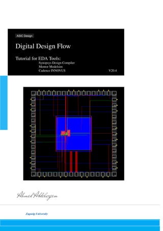
  • 1. Delft University of Technology Code ET4351 Digital Design Flow Tutorial for EDA Tools: Synopsys Design Compiler Mentor Modelsim Cadence INNOVUS V20.4 Ir. A.C. de Graaf Dr.ir. T.G.R.M. van Leuken ASIC Design Zagazig University
  • 2. Preface This document describes the top-down design flow of the implementation a SoC design. Starting from an example HDL description the designer is guided through all the design steps to tapeout GDS2 layout description. This tutorial is derived from "Top-Down digital design flow" version 3.1 (November 2006) by Alain Va- choux, Microelectronic Systems Lab EPFL, Lausanne, Switzerland. i
  • 3. Contents 1 Introduction 1 1.1 Top-down design flow . . . . . . . . . . . . . . . . . . . . . . . . . . . . . . . . . . . . 2 1.2 Design project organization . . . . . . . . . . . . . . . . . . . . . . . . . . . . . . . . . 3 1.3 VHDL example: FIR-Filter . . . . . . . . . . . . . . . . . . . . . . . . . . . . . . . . . 5 1.4 Design flow steps . . . . . . . . . . . . . . . . . . . . . . . . . . . . . . . . . . . . . . . 6 2 VHDL and Verilog simulation 8 2.1 Starting the Modelsim graphical environment . . . . . . . . . . . . . . . . . . . . . . . . 8 2.2 Simulation of (pre-synthesis) RTL VHDL models . . . . . . . . . . . . . . . . . . . . . . 9 2.3 Simulation of the post-synthesis Verilog model with timing data . . . . . . . . . . . . . . 12 2.4 Simulation of the post-route Verilog model with timing data . . . . . . . . . . . . . . . . 14 3 Logic synthesis 15 3.1 Loading and checking the design . . . . . . . . . . . . . . . . . . . . . . . . . . . . . . 15 3.2 Constraining the design . . . . . . . . . . . . . . . . . . . . . . . . . . . . . . . . . . . . 17 3.3 Mapping and Optimization . . . . . . . . . . . . . . . . . . . . . . . . . . . . . . . . . . 17 3.4 Generating reports . . . . . . . . . . . . . . . . . . . . . . . . . . . . . . . . . . . . . . 18 3.5 Check design and generate output . . . . . . . . . . . . . . . . . . . . . . . . . . . . . . 21 4 Standard cell placement and routing 22 4.1 Starting INNOVUS and importing the design . . . . . . . . . . . . . . . . . . . . . . . . 22 4.2 Design import . . . . . . . . . . . . . . . . . . . . . . . . . . . . . . . . . . . . . . . . . 22 4.3 Floorplan Specification . . . . . . . . . . . . . . . . . . . . . . . . . . . . . . . . . . . . 25 4.4 Power ring/stripe creation and routing . . . . . . . . . . . . . . . . . . . . . . . . . . . . 27 4.4.1 Define global net connections . . . . . . . . . . . . . . . . . . . . . . . . . . . . 27 4.4.2 Define power rings . . . . . . . . . . . . . . . . . . . . . . . . . . . . . . . . . . 28 4.4.3 Routing the power grid . . . . . . . . . . . . . . . . . . . . . . . . . . . . . . . . 29 4.5 Core cell placement . . . . . . . . . . . . . . . . . . . . . . . . . . . . . . . . . . . . . 30 4.6 Post-placement timing analysis . . . . . . . . . . . . . . . . . . . . . . . . . . . . . . . 31 4.7 Clock tree synthesis (optional) . . . . . . . . . . . . . . . . . . . . . . . . . . . . . . . . 32 4.8 Filler cell placement . . . . . . . . . . . . . . . . . . . . . . . . . . . . . . . . . . . . . 33 4.9 Design routing . . . . . . . . . . . . . . . . . . . . . . . . . . . . . . . . . . . . . . . . 34 4.10 Post-routing timing optimization and analysis . . . . . . . . . . . . . . . . . . . . . . . . 35 4.11 Design checks . . . . . . . . . . . . . . . . . . . . . . . . . . . . . . . . . . . . . . . . 36 4.12 Report generation . . . . . . . . . . . . . . . . . . . . . . . . . . . . . . . . . . . . . . . 37 4.13 Post-route timing data extraction . . . . . . . . . . . . . . . . . . . . . . . . . . . . . . . 39 4.14 Post-route netlist generation . . . . . . . . . . . . . . . . . . . . . . . . . . . . . . . . . 40 4.15 GDS2 file generation . . . . . . . . . . . . . . . . . . . . . . . . . . . . . . . . . . . . . 41 ii
  • 4. CONTENTS iii 4.16 Using scripts . . . . . . . . . . . . . . . . . . . . . . . . . . . . . . . . . . . . . . . . . 41 A VHDL Netlists 42 A.1 File: filter.vhd . . . . . . . . . . . . . . . . . . . . . . . . . . . . . . . . . . . . . . . . . 42 A.2 File: filter_top.vhd . . . . . . . . . . . . . . . . . . . . . . . . . . . . . . . . . . . . . . 46 A.3 File: filter_soc.vhd . . . . . . . . . . . . . . . . . . . . . . . . . . . . . . . . . . . . . . 48 A.4 File: filter_soc_tb.vhd . . . . . . . . . . . . . . . . . . . . . . . . . . . . . . . . . . . . . 52 B Tool Scripts 55 B.1 Synopsys: Design Compiler . . . . . . . . . . . . . . . . . . . . . . . . . . . . . . . . . 55 B.1.1 setup.tcl . . . . . . . . . . . . . . . . . . . . . . . . . . . . . . . . . . . . . . . . 55 B.1.2 load_design.tcl . . . . . . . . . . . . . . . . . . . . . . . . . . . . . . . . . . . . 56 B.1.3 constraints.tcl . . . . . . . . . . . . . . . . . . . . . . . . . . . . . . . . . . . . . 58 B.1.4 compile.tcl . . . . . . . . . . . . . . . . . . . . . . . . . . . . . . . . . . . . . . 59 B.1.5 check_save.tcl . . . . . . . . . . . . . . . . . . . . . . . . . . . . . . . . . . . . 60 B.1.6 syn.tcl . . . . . . . . . . . . . . . . . . . . . . . . . . . . . . . . . . . . . . . . . 61 B.2 Cadence: INNOVUS . . . . . . . . . . . . . . . . . . . . . . . . . . . . . . . . . . . . . 61 B.2.1 setup.tcl . . . . . . . . . . . . . . . . . . . . . . . . . . . . . . . . . . . . . . . . 61 B.2.2 importDesign.tcl . . . . . . . . . . . . . . . . . . . . . . . . . . . . . . . . . . . 64 B.2.3 floorplan.tcl . . . . . . . . . . . . . . . . . . . . . . . . . . . . . . . . . . . . . . 64 B.2.4 powerplan.tcl . . . . . . . . . . . . . . . . . . . . . . . . . . . . . . . . . . . . . 64 B.2.5 placement.tcl . . . . . . . . . . . . . . . . . . . . . . . . . . . . . . . . . . . . . 66 B.2.6 cts.tcl . . . . . . . . . . . . . . . . . . . . . . . . . . . . . . . . . . . . . . . . . 66 B.2.7 route.tcl . . . . . . . . . . . . . . . . . . . . . . . . . . . . . . . . . . . . . . . . 66 B.2.8 verify.tcl . . . . . . . . . . . . . . . . . . . . . . . . . . . . . . . . . . . . . . . 67 B.2.9 results.tcl . . . . . . . . . . . . . . . . . . . . . . . . . . . . . . . . . . . . . . . 67 B.2.10 par.tcl . . . . . . . . . . . . . . . . . . . . . . . . . . . . . . . . . . . . . . . . . 68
  • 5. Chapter 1 Introduction This document details the typical steps of a top-down digital VHDL/Verilog design flow with the help of a simple design example. The following tools are considered in this document: • Modelsim V10.1f or V10.7c and up, from Mentor Graphics. • Design Compiler and Design Vision SYN_2016.12 or higher from Synopsys. • INNOVUS_17.11.000 or higher from Cadence Design Systems. The design kit used is from IMEC. The process is UMC L65_LL, a 65 nm 8-metal CMOS process. Each of the next chapters in this document is addressing a specific set of tasks. Chapter 2 is about VHDL and Verilog simulation, chapter 3 describes the logic synthesis and chapter 4 describes the place and route steps. All tools have a GUI interface to work interactively, additionally it is possible to use Tcl-scripts. These scripts contain the sequence of individual commands necessary to produce the result of a particular design step and make the designflow reproduceable. Both chapter 3 and 4 start with a description of the interactive way step by step, followed by using a Tcl script doing all the interactive steps in one single step. Throughout this text, commands are displayed with a gray background and the mentioned single step com- mands are additionally framed by a black box. 1
  • 6. CHAPTER 1. INTRODUCTION 2 1.1 Top-down design flow Figure 1.1: Top-down design flow Figure 1.1 illustrates the top-down flow that includes the following steps: VHDL RTL model creation The goal here is to develop synthesizable VHDL models at the RTL level (RTL means Register- Transfer Level). Such models usually define a clear separation between control parts (e.g. finite state machines-FSM) and operative parts (e.g. arithmetic and logic units). Registers are used to store small size data between clock cycles. RAM/ROM memories are used to store large amounts of data or program code. Blocks such as FSMs, ALUs, registers are usually described as behavioral models that do not imply any particular gate-level implementation. Tools used at this step can range from simple text editors to dedicated graphical environments that generate VHDL code automatically. RTL simulation The VHDL RTL models are validated through simulation by means of a number of test-benches also written in VHDL. RTL synthesis The synthesis process infers a possible gate-level realization of the input RTL description that meets user-defined constraints such as area, timings or power consumption. The design constraints are de- fined outside the VHDL models by means of tool-specific commands. The targeted logic gates belong to a library that is provided by a foundry or an IP company as part of a so-called design kit. Typical gate libraries include a few hundreds of combinational and sequential logic gates. Each logic function
  • 7. CHAPTER 1. INTRODUCTION 3 is implemented in several gates to accommodate several fan-out capabilities or drive strengths. The gate library is described in a tool-specific format that defines, for each gate, its function, its area, its timing and power characteristics and its environmental constraints. The synthesis step generates several outputs: a gate-level VHDL net-list, a Verilog gate-level net-list, and a SDF description. The first netlist is typically used for post-synthesis simulation, while the second netlist is better suited as input to the place&route step. The SDF description includes delay information for simulation. Note that considered delays are at this step correct for the gates but only estimated for the interconnections. Post-synthesis gate-level simulation The testbenches used for RTL model validation can be reused (with possibly some modifications to use the VHDL gate-level netlists). The gate-level simulation makes use of VHDL models for the logic gates that are provided in the design kit. These VHDL models follow the VITAL modeling standard to ensure proper back-annotation of delays through the SDF files generated by the synthesis or the place&route step. Standard cell place and route The place&route (P&R) step infers a geometric realization of the gate-level netlist so-called a layout. The standard cell design style puts logic cells in rows of equal heights. As a consequence, all logic gates in the library have the same height, but may have different widths. Each cell has a power rail at its top and a ground rail at its bottom. The interconnections between gates are today usually done over the cells since current processes allow several metal layers (i.e. 8 metal layers for the IMEC L65_LL process). As a consequence, the rows may be abutted and flipped so power and ground rails are shared between successive rows. The P&R step generates several outputs: a geometric description (layout) in GDS2 format, a SDF description and a Verilog gate-level netlist. The SDF description now includes interconnect delay. The Verilog netlist may be different from the one read as input as the P&R step may make further timing optimizations during placement, clock tree generation and routing (e.g. buffer insertion). Post-layout gate-level simulation The Verilog gate-level netlist can be simulated by using the existing VHDL testbenches and the more accurate SDF data extracted from the layout. System-level integration The layout description is then integrated as a block in the designed system. This step is not covered in this document. 1.2 Design project organization First we have to setup a proper work environment. The toolscripts need the CSH shell as command shell while the standard shell after login is the Bash shell. So first we take care that the CSH shell is our default command shell by: cp /opt/eds/DesignLab/bin/dot.bashrc ~/.bashrc Logout and login again. Continue to add the DesignLab script directory to our PATH by: source /opt/eds/DesignLab/bin/dlab.csh
  • 8. CHAPTER 1. INTRODUCTION 4 Given the number of EDA tools and files used in the flow, it is strongly recommended to organize the working environment in a proper way. To that end, the create_eda_project script can be used to create a directory structure in which design files will be stored. The use of the script is as follows: create_eda_project <project-name> where <project-name> is the name of the top-level directory that will host all design files for the projects. For example, to create the project directory called ’filter_umc65’ that will be used to do the tasks presented in the rest of this document, execute the following command: create_eda_project filter_umc65 cd filter_umc65 The filter_umc65 top-level directory hosts the configuration files for logic simulation (Modelsim), logic synthesis (Synopsys DC) and standard cell place and route (Cadence SoC INNOVUS). As a consequence, it is required that the tools are always started from that point. Figure 1.2 shows the proposed directory structure and the role of each subdirectory. The actual use of the subdirectories and files will be explained while going throughout the tutorial in this document. project_name/..........................................................project directory home modelsim.ini...................................................setup file for Modelsim tool DOC...........................................................documentation (pdf, text, etc.) HDL..............................................................VHDL/Verilog source files GATE .................................................................. gate-level netlists RTL....................................................................RTL descriptions TBENCH......................................................................testbenches IP...........................................................external blocks (e.g., memories) LAY..................................................................full-custom layout files LIB.........................................................................design libraries MSIM..................................................Modelsim library (VHDL, Verilog) SNPS...................................................Synopsys library (VHDL, Verilog) PAR......................................................................place & route files BIN...................................................................commands, scripts CONF..................................................................configuration files CTS.............................................................clock tree synthesis files DB ........................................................................ database files DEX................................................................design exchange files LOG............................................................................log files RPT..........................................................................report files SDC.........................................................system design constraint files TEC.....................................................................technology files TIM.........................................................................timing files SIM.........................................................................simulation files BIN...................................................................commands, scripts OUT.........................................................output files (e.g., waveforms) SYN ......................................................................... synthesis files BIN...................................................................commands, scripts DB ........................................................................ database files LOG............................................................................log files RPT..........................................................................report files SDC.........................................................system design constraint files TIM.........................................................................timing files Figure 1.2: Design project structure.
  • 9. CHAPTER 1. INTRODUCTION 5 1.3 VHDL example: FIR-Filter The FIR-Filter example will be used as the reference design throughout the topdown flow. To install the VHDL model and its associated testbenches in the project directory, enter the following command in the top-level project directory filter_umc65: install_design filter_umc65 In order to use the EDA tools and IMEC design kit, a script file called edadk.csh with the necessary PATHs to the tools exists in the directory from which the tools are launched (the top-level project directory). Add these PATHs to your current environment by executing: source edadk.csh For information on the IMEC design kits, find the IMEC documentation in: /opt/eds/DesignKits/IMEC-UMC65/_G-01-LOGIC_MIXED_MODE65N-LL_LOW_K_UMC-IP/doc. Listing 1.1 shows the entity declaration of the VHDL model of a generic 128 tap FIR-Filter. You will find the complete VHDL model including the testbench in Appendix A.1-3. We will call this model the Core. Listing 1.1: Entity declaration of a synthesisable 128 tap FIR-Filter. library ieee; use ieee.std_logic_1164.all; use ieee.numeric_std.all; entity filter_soc is generic ( CWIDTH : integer := 16; CAW : integer := 7; DWIDTH : integer := 16; DAW : integer := 7 ); port ( ClkxCI : in std_logic; ResetxRBI : in std_logic; DataInxDI : in std_logic_vector(DWIDTH -1 downto 0); DataInReqxSI : in std_logic; DataInAckxSO : out std_logic; DataOutxDO : out std_logic_vector(DWIDTH -1 downto 0); DataOutReqxSO : out std_logic; DataOutAckxSI : in std_logic ); end filter_soc;
  • 10. CHAPTER 1. INTRODUCTION 6 Figure 1.3 shows the hierarchy of the filter design. The chiplevel entity named filter_soc consists of compo- nents IO-padcells and the toplevel filter design filter_top. Filter top consists of instances of the components coeff, dataRam and filter. The IO-padcells connect the port signals to the outside world. Filter_top Filter DataRam Coeff Rom Filter_soc Figure 1.3: Hierarchy of the FIR filter chip Listing ?? shows the testbench for the RTL model (file filter_soc_tb.vhd). The testbench for the mapped netlist (file filter_soc_mapped_tb.vhd) can also be used for simulation of both the placed and routed Verilog netlist. The file filter_top.io defines the positions of the IO-padcells for place and route. The file filter_soc_syn.tcl in directory SYN/BIN is a Tcl script that performs synthesis of the VHDL model in batch mode. The file filter_top_par.tcl in directory PAR/BIN is a Tcl script that performs the placement and routing of the synthesized Verilog netlist in batch mode. 1.4 Design flow steps Here are the main steps of the top-down design flow with references to the sections in the document that give more details. Step 1) Pre-synthesis VHDL simulation (tool: Modelsim) 2.1 Compilation of the RTL VHDL model and related testbench [2.2] 2.2 Simulation of the RTL VHDL model Step 2) Logic synthesis (tool: Synopsys Design Compiler) 3.1 RTL VHDL model analysis 3.2 Design elaboration (generic synthesis) 3.3 Design environment definition (operating conditions, wire load model) 3.4 Design constraint definitions (area, clock, timings) [3.2]
  • 11. CHAPTER 1. INTRODUCTION 7 3.5 Design mapping and optimization (mapping to gates) [3.3] 3.6 Report generation [3.4] 3.7 VHDL gate-level netlist generation [3.5] 3.8 Post-synthesis timing data (SDF) generation for the VHDL netlist [3.5] 3.9 Verilog gate-level netlist generation [3.5] 3.10 Design constraints generation for placement and routing [3.5] Step 3) Post-synthesis VHDL simulation (tool: Modelsim) [2.3] 4.1 Compilation of the VHDL/Verilog netlist and related testbench 4.2 Simulation of the post-synthesis gate-level netlist with timing data Step 4) Placement and routing (tool: Cadence INNOVUS) 5.1 Design import (technological data + Verilog netlist) [4.2] 5.2 Floorplan specification [4.3] 5.3 Power ring/stripe creation and routing [4.4] 5.4 Global net connections definition [4.4.1] 5.5 Core cell placement [4.5] 5.6 Post-placement timing analysis [4.6] 5.7 Clock tree synthesis (optional) [4.7] 5.8 Design routing [4.9] 5.9 Post-route timing optimization and analysis [4.10] 5.10 Filler cell placement [4.8] 5.11 Design checks [4.11] 5.12 Report generation [4.12] 5.13 Post-route timing data extraction [4.13] 5.14 Post-route netlist generation [4.14] 5.15 GDS2 file generation [4.15] Step 5) Post-layout VHDL/Verilog simulation (tool: Modelsim) [2.4] 6.1 Compilation of the Verilog netlist and related testbench 6.2 Simulation of the post-synthesis or post-P&R gate-level netlist with PaR timing data
  • 12. Chapter 2 VHDL and Verilog simulation This chapter presents the main steps to perform the logic simulation of VHDL and Verilog models with the Modelsim tool. 2.1 Starting the Modelsim graphical environment To start the Modelsim environment, create first a work library in de directory LIB/MSIM then enter in the vsim command in the Unix shell: vlib LIB/MSIM/work vmap work LIB/MSIM/work/ vsim -voptargs=+acc & Figure 2.1: Modelsim console window 8
  • 13. CHAPTER 2. VHDL AND VERILOG SIMULATION 9 The modelsim.ini file actually defines the mapping between logical design libraries and their physical locations. Note that the Help menu on the top right allows one to access the complete documentation of the tool. After having started the vsim GUI you have to compile all the VHDL source of your design into the simulation library work. Now you have two options to simulate your model, either interactively or by executing the following convenience scripts (see directory SIM/BIN) on the VSIM command line: wave.do To start a wave window with the ports of the top level module. start_msim[_mapped | _routed ].do To start up the simulation of the particular module. run_msim[_mapped | _routed ].do To load the filter coefficients into the coefficient ROM and runs the simulation for 300 us. 2.2 Simulation of (pre-synthesis) RTL VHDL models The task here is to validate the functionality of the VHDL model that will be synthesized. The first step is to compile the VHDL model and its associated testbench. There are two ways to compile VHDL models. One way is to execute the vcom command from the command line of the Modelsim window: ModelSim> vlog -quiet HDL/RTL/SYKA65_128X16X1CM2.v ModelSim> vlog -quiet HDL/RTL/SPKA65_512X16BM1A.v ModelSim> vcom -quiet HDL/RTL/coeffFAR.vhd ModelSim> vcom -quiet HDL/RTL/dataRamFAR.vhd ModelSim> vcom -quiet HDL/RTL/filter.vhd ModelSim> vcom -quiet HDL/RTL/filter_top.vhd ModelSim> vcom -quiet HDL/RTL/filter_soc.vhd ModelSim> vcom -quiet -suppress 1288,1074,1194 HDL/TBENCH/filter_soc_tb.vhd or alternatively execute the shell script compile_msim.sh from the CSH command line: sh compile_msim.sh The second way is to left-click on the Compile icon , to select the files to compile in the HDL/RTL and HDL/TBENCH directories, click on Compile and finally close the window (click Done). The compiled modules are stored in the logical library WORK which is mapped to the physical location LIB/MSIM/work. Once VHDL (or Verilog) mod- els have been successfully compiled in the design library, it is possible to create a make file that can be used to recompile only the required files. The vmake command can only be run from a Unix shell and creates the make file: vmake > Makefile The created file Makefile now defines the design unit dependencies and the compilation commands to recompile only those source files that have been modified or that depend on modified files. To rebuild the library, run the make command in the Unix shell To simulate the RTL model, select the main menu item 1. Select the main menu item Simulate ⇒ Start simulation... to get the simulation dialog window. 2. Select from library work the architecture of the testbench and a resolution of 1ns.
  • 14. CHAPTER 2. VHDL AND VERILOG SIMULATION 10 3. Click the Libraries tab to add the gate library umc65_generic_core 4. Unselect Énable optimization´ (off) . 5. Then click OK. The main window now changes a bit to show the simulation hierarchy, the list of signals in the testbench and the simulation console (with now the VSIM number> prompt). Left clicking twice on an instance in the simulation hierarchy pane displays the corresponding VHDL source in the right pane.
  • 15. CHAPTER 2. VHDL AND VERILOG SIMULATION 11 The next step is to select the signals to display in simulation. Right click in the Objects (top center) pane, then select Add to Wave ⇒ Signals in Region. Note that the appropriate hierarchy level is selected in the simu- lation hierarchy window. Selecting another level, e.g. dut, will display all the signals visible in this scope. You may want to add selected signals from inner levels (local signals). The selected signals are displayed in a new window called wave. The wave pane is by default located on the top right (as a new tab on the source windows). You can click on the Undock icon to make the wave pane separate. Now first load the content coefficient file into the coefficient memory: VSIM 7> run 35 ns VSIM 7> do SIM/BIN/load.do Then to start the simulation, it is either possible to enter run commands in the simulation console such as: VSIM 7> run 300 us or to click on the Run icon in the main window or in the wave window. The signal waveforms are then visible in the wave window. To change the radix of the displayed signals, select the signals (press shift left-click for multiple selection), then select the wave menu item Format ⇒ Radix ⇒ Unsigned. Note that the command run -all runs the simulation until there is no more pending event in the simulation queue. This could lead to never ending simulation when the model, like the testbench loaded here, has a continuously switching signal such as the clock signal clk. It is however possible to stop the current simu- lation by clicking the Break icon in the main window or in the wave window. Run the simulation interactively as described in the previous section or run the following scripts (See SIM/BIN) from the VSIM command line. VSIM 7> do SIM/BIN/start_msim.do VSIM 8> do SIM/BIN/wave.do VSIM 9> do SIM/BIN/run_msim.do If you make any modification to the VHDL source, you need to recompile the sources (manually or using the vmake command described earlier in this section), and then restart the simulation in the same environment (e.g., the same displayed waveforms or the same simulation breakpoints) with the restart -f command.
  • 16. CHAPTER 2. VHDL AND VERILOG SIMULATION 12 2.3 Simulation of the post-synthesis Verilog model with timing data This step occurs after the RTL model has been synthesized into a gate-level netlist. The timing informa- tion about the design which includes the delay of the library cells only is stored in a SDF file. (See -3.5 VHDL/Verilog gate-level netlist generation and post-synthesis timing data (SDF) extraction.) Compile the Verilog gate-level netlist generated by the logic synthesis and its testbench in a new library called mapped: vlib LIB/MSIM/mapped vmap mapped LIB/MSIM/mapped/ ModelSim> vlog -quiet HDL/RTL/SYKA65_128X16X1CM2.v ModelSim> vlog -quiet HDL/RTL/SPKA65_512X16BM1A.v ModelSim> vlog -work LIB/MSIM/mapped HDL/GATE/filter_soc_mapped.v ModelSim> vcom -work LIB/MSIM/mapped HDL/TBENCH/filter_soc_tb_mapped.vhd or execute the shell script compile_msim_mapped.sh. To simulate the RTL model, 1. Select the main menu item Simulate ⇒ Start simulation... to get the simulation dialog window. 2. Select from library mapped the architecture of the testbench and a resolution of 100ps. 3. Click the Libraries tab to add the gate library umc65_generic_core
  • 17. CHAPTER 2. VHDL AND VERILOG SIMULATION 13 4. Then click the SDF tab. In the SDF dialog window, add the file SYN/TIM/filter_soc_mapped.sdf and specify the region dut, which is the label of the instance in the testbench that will be annotated with timing data. Note that the Reduce SDF errors to warnings box must be checked. This is required to avoid the simulation to stop prematurely due to errors such as "Failed to find port ´a(7)´". These are not really errors here as they are related to interconnect delay data in the SDF file that are not used in the simulation (they are actually all set to zero). Then click OK in the remaining Start Simulation dialog box to load the mapped netlist. Clock to output delays of the order of 100ps to 1ns should be visible in the wave window. Run the simulation interactively as described in the previous section or run the following scripts (See SIM/BIN) from the VSIM command line. VSIM 7> do SIM/BIN/start_msim_mapped.do VSIM 8> do SIM/BIN/wave.do VSIM 9> do SIM/BIN/run_msim_mapped.do
  • 18. CHAPTER 2. VHDL AND VERILOG SIMULATION 14 2.4 Simulation of the post-route Verilog model with timing data This step occurs after the design has been placed and routed. The Post-route SDF-file contains cell delay and wire delays of the circuit. See "4.13 Post-route timing data extraction" and "4.14 Post-route netlist generation". This step involves the simulation of a Verilog gate-level netlist with a VHDL testbench. Com- pile the Verilog gate-level netlist generated by the logic synthesis and its testbench in a new library called routed: vlib LIB/MSIM/routed vmap routed LIB/MSIM/routed/ ModelSim> vlog -quiet HDL/RTL/SYKA65_128X16X1CM2.v ModelSim> vlog -quiet HDL/RTL/SPKA65_512X16BM1A.v ModelSim> vlog -work LIB/MSIM/routed HDL/GATE/filter_soc_routed.v ModelSim> vcom -work LIB/MSIM/routed HDL/TBENCH/filter_soc_tb_mapped.vhd or execute the shell script compile_msim_routed.sh. To simulate the placed and routed netlist with timing data: 1. Select the item Simulate ⇒ Start simulation... in the main menu to get the simulation dialog win- dow. 2. Select from library routed the architecture of the testbench and a resolution of 100ps. 3. Then click the Libraries tab to add the gate library umc65_generic_core 4. Load the SDF timing file PAR/TIM/filter_soc_routed.sdf. Note that the Reduce SDF errors to warnings box must be checked. This is required to avoid the sim- ulation to stop prematurely due to errors such as “Failed to find matching specify timing constraint”. These are not really errors here as they are related to removal (asynchronous) timing constraints generated by INNOVUS that are not supported in the Verilog models of the gates. Run the simulation interactively or run the following scripts (See SIM/BIN) from the VSIM command line. VSIM 7> do SIM/BIN/start_msim_routed.do VSIM 8> do SIM/BIN/wave.do VSIM 9> do SIM/BIN/run_msim_routed.do
  • 19. Chapter 3 Logic synthesis This chapter presents the main steps to perform the logic synthesis of the VHDL RTL model with the Synopsys Design Compiler tool. Design Compiler(DC) supports Tcl scripts. Scripts are useful to capture the intermediate steps in the synthesis flow and make the flow reproducable. All scripts for synthesis are found in the directory SYN/BIN. 3.1 Loading and checking the design 1. Start the Synopsys DC_Shell GUI , enter the following command command in a new shell: dc_shell -gui The command line is also echoed in the terminal shell from which the tool has been started, so it is possible to enter DC commands from there as well. It is still possible to execute some Unix commands from here. 15
  • 20. CHAPTER 3. LOGIC SYNTHESIS 16 2. Load the libraries and initialize global variables source SYN/BIN/setup.tcl 3. Load the design During this phase the RTL source is analyzed and elaborated. source SYN/BIN/load_design.tcl The analysis phase compiles the VHDL model and checks that the VHDL code is synthesizable. The elaboration phase performs a generic pre-synthesis of the analyzed model. It essentially identifies the registers that will be inferred. The console now displays the inferred registers and the kind of reset (here asynchronous reset - AR: Y). Listing 3.1: "Elaborate design command" design_vision> elaborate FILTER_SOC -architecture RTL -library WORK -parameters "CWIDTH = 16, CAW = 7, DWIDTH = 16, DAW = 7, CWIDTH = 16" . . Inferred memory devices in process in routine filter_DWIDTH16_DAW7 line 158 in file ’/mnt/tango/md2/users/sander/ET4351/asic/designs/filter1/HDL/RTL/filter. vhd’. ========================================================================== | Register Name | Type | Width | Bus | MB | AR | AS | SR | SS | ST | ========================================================================== | OutRegxDP_reg | Flip-flop | 16 | Y | N | Y | N | N | N | N | ========================================================================== . . dc_shell> Current design is ’filter_soc_CWIDTH16_CAW7_DWIDTH16_DAW7’. Note the name filter_soc_CWIDTH16_CAW7_DWIDTH16_DAW7 given to the elaborated entity.
  • 21. CHAPTER 3. LOGIC SYNTHESIS 17 It is possible to display the elaborated schematic by selecting the entity i_filter_top in the hierarchy window and then clicking the Create Schematic button. You can the browse the hierarchy with the the up/down buttons in the top menu. . Note that the symbols merely indicate generic components that do not yet represent any real logic gate. It is common practice to save the result of intermediate steps into a database restore file so next steps can be taken up from such restore point. Here the result after elaboration is stored into file: SYN/DB/filter_soc_elab.ddc 3.2 Constraining the design Load the (Ideal Clock) timing constraints source SYN/BIN/constraints.tcl Many kinds of constraints may be defined on the design. Here only constraints on the area and the clock will be defined. To define the clock attributes, i.e. its period and duty cycle, Define a clock period of 10 ns with 50% duty cycle. Time unit is not specified here. It is defined in the cell library and is usually ns. A max area constraint set to zero is not realistic but it will force the synthesizer to target a minimum area. set_max_area 0 3.3 Mapping and Optimization The optimization phase, also called here compilation phase, is technology dependent. It performs the assignment of logic gates from the standard cell library to the elaborated design in such a way the defined constraints are met. Note that the default resource allocation and implementation for operative parts is based on timing constraints. This means that resource sharing is used so that timing constraints are met or not worsened. Perform the mapping and optimization process:
  • 22. CHAPTER 3. LOGIC SYNTHESIS 18 source SYN/BIN/compile.tcl The mapped design schematic includes instances of the coefficient rom, data ram and the filter circuit. Also, the cells are now real gates from the cell library. The mapped design will be saved into file SYN/DB/filter_soc_mapped.ddc. 3.4 Generating reports It is possible to get many reports on various synthesis results. Here only reports on the area used, critical path timing and the resources used will be generated. We can check the quality of the design with the following commands: report_qor report_timing report_area
  • 23. CHAPTER 3. LOGIC SYNTHESIS 19 **************************************** Report : timing -path full -delay max -max_paths 1 -sort_by group Design : filter_soc Version: M-2016.12 Date : Tue Jul 10 14:34:13 2018 **************************************** Operating Conditions: uk65lscllmvbbr_108c125_wc Library: uk65lscllmvbbr_108c125_wc Wire Load Model Mode: top Startpoint: DataInReqxSI (input port clocked by ClkxCI) Endpoint: i_filter_top/i_filter/RamWritexDO_reg [0] (rising edge -triggered flip -flop clocked by ClkxCI) Path Group: ClkxCI Path Type: max Des/Clust/Port Wire Load Model Library ------------------------------------------------ filter_soc wl0 uk65lscllmvbbr_108c125_wc Point Incr Path -------------------------------------------------------------------------- clock ClkxCI (rise edge) 0.00 0.00 clock network delay (ideal) 0.00 0.00 input external delay 0.00 0.00 r DataInReqxSI (in) 5.38 5.38 r i_DataInReqxSI/PAD (IUMA) 0.00 5.38 r i_DataInReqxSI/DI (IUMA) 1.73 7.10 r U418/Z (ND3M8RA) 0.12 7.22 f U424/Z (CKMUX2M2R) 0.17 7.39 r i_filter_top/i_filter/RamWritexDO_reg [0]/D (DFQRM1RA) 0.00 7.39 r data arrival time 7.39 clock ClkxCI (rise edge) 8.00 8.00 clock network delay (ideal) 0.00 8.00 clock uncertainty -0.20 7.80 i_filter_top/i_filter/RamWritexDO_reg [0]/CK (DFQRM1RA) 0.00 7.80 r library setup time -0.04 7.76 data required time 7.76 -------------------------------------------------------------------------- data required time 7.76 data arrival time -7.39 -------------------------------------------------------------------------- slack (MET) 0.38 1 All times are expressed in ns (the time unit is defined in the cell library). The slack defines the time margin from the clock period. A positive slack means that the latest arriving signal in the path still arrives before the end of the clock period. A negative slack means that the timing constraint imposed by the clock is violated. The timing delays that are accounted for are the internal gate delays (from the cell library) and the estimated interconnect delays (from the cell library and the wire load model in use).
  • 24. CHAPTER 3. LOGIC SYNTHESIS 20 ∗∗∗∗∗∗∗∗∗∗∗∗∗∗∗∗∗∗∗∗∗∗∗∗∗∗∗∗∗∗∗∗∗∗∗∗∗∗∗∗ Report : power −a n a l y s i s _ e f f o r t low Design : f i l t e r _ s o c Version : M−2016.12 Date : Tue J u l 10 14:34:13 2018 ∗∗∗∗∗∗∗∗∗∗∗∗∗∗∗∗∗∗∗∗∗∗∗∗∗∗∗∗∗∗∗∗∗∗∗∗∗∗∗∗ Libr ary ( s ) Used : uk65lscllmvbbr_108c125_wc ( F i l e : / opt / eds / DesignKits /IMEC−UMC65/ _G−01− LOGIC_MIXED_MODE65N−LL_LOW_K_UMC −IP / synopsys / uk65lscllmvbbr_108c125_wc . db ) SYKA65_128X16X1CM2_BC ( F i l e : / opt / eds / DesignKits /IMEC−UMC65/ Memories / SYKA65_128X16X1CM2 / SYKA65_128X16X1CM2_BC . db ) SPKA65_512X16BM1A_BC ( F i l e : / opt / eds / DesignKits /IMEC−UMC65/ Memories / SPKA65_512X16BM1A / SPKA65_512X16BM1A_BC . db ) u065gioll25mvir_25_wc ( F i l e : / opt / eds / DesignKits /IMEC−UMC65/ _G−01− LOGIC_MIXED_MODE65N−LL_LOW_K_UMC −IP / synopsys / u065gioll25mvir_25_wc . db ) Operating Conditions : uk65lscllmvbbr_108c125_wc Li brary : uk65lscllmvbbr_108c125_wc Wire Load Model Mode : top Design Wire Load Model Librar y −−−−−−−−−−−−−−−−−−−−−−−−−−−−−−−−−−−−−−−−−−−−−−−− f i l t e r _ s o c wl0 uk65lscllmvbbr_108c125_wc Global Operating Voltage = 1.08 Power−s p e c i f i c u n i t i n f o r m a t i o n : Voltage Units = 1V Capacitance Units = 1.000000 pf Time Units = 1 ns Dynamic Power Units = 1mW ( derived from V, C, T u n i t s ) Leakage Power Units = 1pW Cell I n t e r n a l Power = 698.0497 uW (61%) Net Switching Power = 440.4088 uW (39%) −−−−−−−−− Total Dynamic Power = 1.1385 mW (100%) Cell Leakage Power = 3.9863 uW I n t e r n a l Switching Leakage Total Power Group Power Power Power Power ( % ) A t t r s −−−−−−−−−−−−−−−−−−−−−−−−−−−−−−−−−−−−−−−−−−−−−−−−−−−−−−−−−−−−−−−−−−−−−−−−−−−−−−−−−−−−−−−−−−−−−−−−−− io_pad 0.2371 0.4126 6.2701 e+05 0.6504 ( 56.93%) memory 0.3775 1.8190 e−03 2.9396 e+06 0.3822 ( 33.46%) black_box 0.0000 0.0000 0.0000 0.0000 ( 0.00%) clock_network 0.0000 0.0000 0.0000 0.0000 ( 0.00%) r e g i s t e r 5.6930 e−02 1.1159 e−03 1.0277 e+05 5.8149 e−02 ( 5.09%) s e q u e n t i a l 0.0000 0.0000 0.0000 0.0000 ( 0.00%) combinational 2.6514 e−02 2.4832 e−02 3.1690 e+05 5.1663 e−02 ( 4.52%) −−−−−−−−−−−−−−−−−−−−−−−−−−−−−−−−−−−−−−−−−−−−−−−−−−−−−−−−−−−−−−−−−−−−−−−−−−−−−−−−−−−−−−−−−−−−−−−−−− Total 0.6980 mW 0.4404 mW 3.9863 e+06 pW 1.1424 mW 1
  • 25. CHAPTER 3. LOGIC SYNTHESIS 21 3.5 Check design and generate output 1. Check the design and save the netlist: source SYN/BIN/check_save.tcl During this step diverse output files are generated: • First several reports (in text format) are written into directory SYN/RPT. Read them, because they contain valuable information related to the design. • Second a Verilog model of the mapped design for simulatiom and for use Place and Route is written into file HDL/GATE/filter_soc_mapped.v. • Third a SDF (Standard Delay Format) file is gereated that includes the gate delays. Care should be taken to use the right naming scheme when generating the SDF file, otherwise the back- annotation of the delays onto the Verilog netlist for simulation will fail. The SDF file is stored into file SYN/TIM/filter_soc_mapped.sdf. Information: Annotated ’cell’ delays are assumed to include load delay. The informational message says that the estimated interconnect delays are actually included in the SDF file as part of the cell delays. The generated SDF file actually includes a list of interconnect delays of zero values. • Fourth a SDC (Synopsys Design Constraint) file SYN/SDC/filter_soc_mapped.sdc is written. Both design environment and design constraint definitions are stored in a format that can be read by other Synopsys tools such as PrimeTime or other EDA tool such as Cadence INNOVUS. It is much more convenient to use scripts and to run the synthesis tool in batch mode when the design complexity increases. Scripts also conveniently capture the synthesis flow and make it reusable. Synopsys Design Compiler supports the Tcl language for building scripts. An example of such a script for the synthesis of the filter_soc design has been installed in the directory SYN/BIN The script has to run from the project top directory and it assumes a directory organization as described in section 1.2. To run the Tcl script, execute the following command in a Unix shell: dc_shell -f SYN/BIN/syn.tcl When the script finishes executing, the dc_shell environment is still active so you can enter other dc_shell commands. Enter quit or exit to return to the Unix shell.
  • 26. Chapter 4 Standard cell placement and routing This chapter presents the main steps to perform the placement and the routing of the synthesized gate- level netlist using standard cells from the IMEC design kit. The tool used here is Cadence Innovus. Each subsection describes a particular step in the place and route process, first by how to do this manually then by using a TCL script. 4.1 Starting INNOVUS and importing the design To start the INNOVUS environment, enter the innovus command in a new Unix shell: innovus If the -overwrite switch is not used, both log and command files are incremented at each new session. The Unix shell from which the tool is started is called the Innovus console. The console displays the innovus> prompt. This is where you can enter all Innovus text commands and where the tool displays messages. If you use the console for other actions, e.g., Unix commands, the Innovus session suspends until you finish the action. The first action to perform is loading a setup script that contains statements to set several global variables and definitions of the used grid. source PAR/BIN/setup.tcl 4.2 Design import Importing the design into Innovus involves specifying the following setup information: Design libraries and files. This includes information on the technological process and the cell library in the LEF (Layout Exchange Format) format. LEF files provides information such as metal and via layers and via generate rules which is used for routing tasks. They also provide the minimum infor- mation on cell layouts for placement and routing. Gate-level netlist. This relates to the synthesized (Verilog) netlist to be placed and routed. Timing libraries. This includes information on the cell timings (delays, setup/hold times, etc.). 22
  • 27. CHAPTER 4. STANDARD CELL PLACEMENT AND ROUTING 23 To start the design import, select: File ⇒ Import Design... Click Load... Select PAR/CONF/umc65_init.globals Click OK Loading the file umc65_init.globals set the Verilog source file to "filter_soc_mapped.v". The imported design contains two core macro’s (coeff, ram) on the right side of the chip. The main window includes three different design views that you can toggle during a session: the Floorplan view, the Amoeba view, and the Physical view. The Floorplan view displays the hierarchical module and block guides, connection flight lines, and floorplan objects, including block placement, and power/ground nets. The Amoeba view displays the outline of the modules and submodules after placement, showing physical locality of the module. The Physical view displays the detailed placements of the module’s blocks, standard cells, nets, and interconnects. The main window includes a satellite window, which identifies the location of the current view in the design display area, relative to the entire design. The chip area is identified by a yellow box, the satellite view is identified by the pink crossbox. When you display an entire chip in the design display area, the satellite crossbox encompasses the chip area yellow box. When you zoom and pan through the chip in the design display area, the satellite crossbox identifies where you are relative to the entire chip. • To move to an area in the design display area, click and drag on the satellite crossbox.
  • 28. CHAPTER 4. STANDARD CELL PLACEMENT AND ROUTING 24 • To select a new area in the design display area, click and drag on the satellite crossbox. • To resize an area in the satellite window, click with the Shift key and drag a corner of the crossbox. • To define a chip area in the satellite window, right-click and drag on an area. There are a number of binding keys available (hit the key when the Innovus GUI is active): b display the list of binding keys d (de)select or delete objects f zoom the display to fit the core area k create a ruler K remove last ruler displayed q display the object attribute editor form for the selected object; click the left-button mouse to select an object, Shift-click to select or deselect an object u undo last command U redo last command z zoom-in 2x Z zoom-out 2x Arrows pan the display. Hit CTRL-R to refresh the display. The alternative way instead of using the interactive environment is loading the following script in the console window. source PAR/BIN/importDesign.tcl
  • 29. CHAPTER 4. STANDARD CELL PLACEMENT AND ROUTING 25 4.3 Floorplan Specification The floorplan defines the actual shape, or aspect ratio, the layout will take, the global and detailed routing grids, the rows to host the core cells and the I/O pad cells, and the location of the corner cells. Have a look at the IO configuration file PAR/CONF/filter_soc.io. Start floorplanning by selecting from the main menu: Floorplan ⇒ Specify Floorplan... Enter the details so that the form looks the same as the one below: Click OK Now you can place the macros on the right side of the chip by hand through selecting the red-circle item on the menu bar and drag the particular macro into the core area. Or you can select from the main menu floorplanning: Floorplan ⇒ Automatic Floorplan ⇒ Plan Design... In TAB "Set Plan Design Mode" Uncheck Boundary Place Click OK Floorplan ⇒ Edit Floorplan ⇒ Edit Floorplan... halo’s around the macro cell can be specified to pre- vent placement of standardcells to close to the macro cells. Specify here a halo width of 28 um and leave everything else default. Floorplan ⇒ Clear Floorplan... allows you to delete all or parts of the floorplan objects. Now the gaps between the IO cells must be filled with IO-filler cells. Execute the fillperi.tcl script by the following command on the command line: source PAR/BIN/fillperi.tcl
  • 30. CHAPTER 4. STANDARD CELL PLACEMENT AND ROUTING 26 The display design area pane now shows the defined floorplan with the required number of rows. It is a good idea to save the design at that stage to allow restarting here quickly without needing to redo all the previous steps. Select: File ⇒ Save Design...
  • 31. CHAPTER 4. STANDARD CELL PLACEMENT AND ROUTING 27 Check innovus in de popup-menu and save the current state in the file PAR/DB/filter_soc-fplan1 The data are actually saved in the directory PAR/DB/filter_soc-fplan1.dat To restore design data, select File ⇒ Restore Design... in the main menu and select the particular design file to restore from the PAR/DB directory. The following script performs all the above steps: source PAR/BIN/floorplan.tcl 4.4 Power ring/stripe creation and routing This step defines the pins and nets connected to global power and ground nets. Additionally the VDD and VSS power rings around the core and macros are generated and optionally adds a number of vertical and/or horizontal power stripes across the core. Stripes ensure a proper power distribution in large cores. They are not strictly required here as the design is small. 4.4.1 Define global net connections This step assigns pins or nets to global power and ground nets. The imported Verilog netlist does not mention any power and ground connections. However, the cells that will be placed do have power/ground pins that will need to be routed to the global power/ground nets defined for the block. Select Power ⇒ Connect Global Nets... in the main menu. The left pane (Connection List) is initially empty. For each VDD and VSS net do: In the Connect field check Pin and enter at Pin Name(s) (Here VDD or VSS). In the Scope field check Apply All Fill in the To Global Net field either VDD or VSS. Click on Add to List. The left pane now includes the related global net connection. Repeat these actions with Tie High checked and finally with Tie Low checked. Click on Apply and close the window by Cancel. Or execute the script: source PAR/BIN/global_nets.tcl
  • 32. CHAPTER 4. STANDARD CELL PLACEMENT AND ROUTING 28 4.4.2 Define power rings Select Power ⇒ Power Planning ⇒ Add Rings... in the main menu. The Net(s) field defines the number and the kinds of rings from the core. In our case, there will be first a ground ring around the core and a VDD ring around the ground ring. The net names should be consistent with the power net names in the cell LEF file. In the field Ring Type: Check Core ring(s) contouring. In the filed Ring Configuration: Specify ring widths of 2.8 µm spaced by 2.8 µm with offset of 28 µm. The rings can be placed either at a particular offset as specified in our case or in the center of the channel between the core and the chip boundary (or the IO pads, if any) by checking Offset: Center in channel. It is possible to extend the ring segments to reach the core boundary. Click on the Advanced tab and click on the segments you’d like to extend. Other power and ground side trunks can be defined by selecting only horizontal or vertical segments. Click OK to generate the rings. To add block rings around the macro blocks, select Power ⇒ Power Planning ⇒ Add Rings... in the main menu. In the field Ring Type: check Block ring(s) around. In the field Ring Configuration Specify ring widths of 3 µm spaced by 2 µm with offset of 1µm.
  • 33. CHAPTER 4. STANDARD CELL PLACEMENT AND ROUTING 29 Click OK to generate the block rings. To add power stripes, select Power ⇒ Power Planning ⇒ Add Stripes... in the main menu. The Set Configuration area defines the Net(s) pattern, direction, layer, width and spacing of the stripes. Our example does not need any stripes so click Cancel 4.4.3 Routing the power grid Now, it is possible to route the power grid. Select Route ⇒ SRoute... in the main menu. All default values are fine. Click OK to do the routing. The design now looks like below: It is recommended to save the new stage of the design. Select File ⇒ Save Design... in the main menu and save the current state in the file PAR/DB/filter_soc-pplan. The alternative to execute the above powerplan steps manually is to execute the script: source PAR/BIN/powerplan.tcl
  • 34. CHAPTER 4. STANDARD CELL PLACEMENT AND ROUTING 30 4.5 Core cell placement This step places the cells of the imported Verilog netlist in the rows. Select Place ⇒ Standard Cells... in the main menu. By clicking the Mode button one can specify placement options. By default it will run in Timing Driven Placement Mode. Stick to the default options and click OK. The Timing Driven Placement Mode option will optimize the placement of the cells that are on the critical path. Some cell instances may be replaced with cells having lower driving capabilities (downsizing) or stronger driving capabilities (upsizing). Buffers may be also added or deleted. The Innovus console notifies such changes. Click OK to do the placement. It may take some time to complete, especially when the placement is timing driven and a high effort level is used . The placement should then look like below: It is recommended to save the new stage of the design. Select File ⇒ Save Design... in the main menu and save the current state in the file PAR/DB/filter_soc-placed. The alternative way is by running the tcl script: source PAR/BIN/placement.tcl
  • 35. CHAPTER 4. STANDARD CELL PLACEMENT AND ROUTING 31 4.6 Post-placement timing analysis The timing analysis engine in Innovus can now be run to get a relatively good idea of the timing perfor- mances of the design. It actually performs a trial routing and a parasitic extraction based on the current cell placement. Select Timing ⇒ Report Timing... in the main menu. Define the path for the slack report file. Click OK. In the Innovus console window you get a summary of the timing analysis: ############################################################### # Generated by: Cadence Innovus 17 .11−s080_1 # OS: Linux x86_64 ( Host ID s a l s a ) # Generated on: Wed Jul 4 13 :32:40 2018 # Design: f i l t e r _ s o c # Command: timeDesign −preCTS −pathReports −drvReports −slackReports −numPaths 50 −prefix f i l t e r _ s o c _ p r e C T S −outDir PAR / RPT ############################################################### −−−−−−−−−−−−−−−−−−−−−−−−−−−−−−−−−−−−−−−−−−−−−−−−−−−−−−−−−−−− timeDesign Summary −−−−−−−−−−−−−−−−−−−−−−−−−−−−−−−−−−−−−−−−−−−−−−−−−−−−−−−−−−−− +−−−−−−−−−−−−−−−−−−−−+−−−−−−−−−+−−−−−−−−−+−−−−−−−−−+ | Setup mode | a l l | reg2reg | default | +−−−−−−−−−−−−−−−−−−−−+−−−−−−−−−+−−−−−−−−−+−−−−−−−−−+ | WNS ( ns ) : | −0.109 | 1 .215 | −0.109 | | TNS ( ns ) : | −1.616 | 0 .000 | −1.616 | | V i o l a t i n g P a t h s : | 17 | 0 | 17 | | All P a t h s : | 113 | 95 | 36 | +−−−−−−−−−−−−−−−−−−−−+−−−−−−−−−+−−−−−−−−−+−−−−−−−−−+ +−−−−−−−−−−−−−−−−+−−−−−−−−−−−−−−−−−−−−−−−−−−−−−−−+−−−−−−−−−−−−−−−−−−+ | | Real | Total | | DRVs +−−−−−−−−−−−−−−−−−−+−−−−−−−−−−−−+−−−−−−−−−−−−−−−−−−| | | Nr n e t s ( terms ) | Worst Vio | Nr n e t s ( terms ) | +−−−−−−−−−−−−−−−−+−−−−−−−−−−−−−−−−−−+−−−−−−−−−−−−+−−−−−−−−−−−−−−−−−−+ | max_cap | 24 (24) | −0.126 | 25 (25) | | max_tran | 24 (135) | −3.097 | 24 (135) | | max_fanout | 0 ( 0 ) | 0 | 0 ( 0 ) | | max_length | 0 ( 0 ) | 0 | 0 ( 0 ) | +−−−−−−−−−−−−−−−−+−−−−−−−−−−−−−−−−−−+−−−−−−−−−−−−+−−−−−−−−−−−−−−−−−−+ D e n s i t y : 0 .383% Routing Overflow: 0 .00% H and 0 .00% V −−−−−−−−−−−−−−−−−−−−−−−−−−−−−−−−−−−−−−−−−−−−−−−−−−−−−−−−−−−−
  • 36. CHAPTER 4. STANDARD CELL PLACEMENT AND ROUTING 32 The design is critical as the worst negative slack (WNS) is negative (-0.109 ns). To get more details on the critical path execute the following commands in the Innovus console: report_timing > PAR/RPT/filter_soc_preCTS-reportTiming The following report is then displayed in the console: ############################################################### # Generated by: Cadence Innovus 17 .11−s080_1 # OS: Linux x86_64 ( Host ID s a l s a ) # Generated on: Wed Jul 4 13 :42:29 2018 # Design: f i l t e r _ s o c # Command: r e p o r t _ t i m i n g > PAR / RPT / filter_soc_preCTS−reportTiming ############################################################### Path 1 : VIOLATED Setup Check with Pin i _ f i l t e r _ t o p _ i _ f i l t e r _ S t a t e x D P _ r e g _ 0 _ /CK Endpoint: i _ f i l t e r _ t o p _ i _ f i l t e r _ S t a t e x D P _ r e g _ 0 _ /D ( ^ ) checked with l e a d i n g edge of ’ ClkxCI ’ B e g i n p o i n t : DataInReqxSI ( ^ ) t r i g g e r e d by l e a d i n g edge of ’ ClkxCI ’ Path Groups: { ClkxCI } Analysis View: minView Other End A r r i v a l Time 0 .000 − Setup 0 .109 + Phase S h i f t 8 .000 − U n c e r t a i n t y 0 .200 = Required Time 7 .691 − A r r i v a l Time 7 .800 = Slack Time −0.109 Clock Rise Edge 0 .000 + Input Delay 0 .000 + Drive Adjustment 5 .437 = Beginpoint A r r i v a l Time 5 .437 +−−−−−−−−−−−−−−−−−−−−−−−−−−−−−−−−−−−−−−−−−−−−−−−−−−−−−−−−−−−−−−−−−−−−−−−−−−−−−−−−−−−−−+ | I n s t a n c e | Arc | Cell | Delay | A r r i v a l | Required | | | | | | Time | Time | |−−−−−−−−−−−−−−−−−−−−−−−−−−−+−−−−−−−−−−−−−−−−+−−−−−−−−−−−+−−−−−−−+−−−−−−−−−+−−−−−−−−−−| | | DataInReqxSI ^ | | | 5 .437 | 5 .328 | | i_DataInReqxSI | PAD ^ −> DI ^ | IUMA | 1 .818 | 7 .254 | 7 .146 | | U418 | A ^ −> Z v | ND3M8RA | 0 .383 | 7 .637 | 7 .528 | | U171 | B v −> Z ^ | OAI211M1R | 0 .163 | 7 .800 | 7 .691 | | i _ f i l t e r _ t o p _ i _ f i l t e r _ | D ^ | DFQRM1RA | 0 .000 | 7 .800 | 7 .691 | | i _ f i l t e r _ S t a t e x D P _ r e g _ 0 _ | D ^ | DFQRM1RA | 0 .000 | 7 .800 | 7 .691 | +−−−−−−−−−−−−−−−−−−−−−−−−−−−−−−−−−−−−−−−−−−−−−−−−−−−−−−−−−−−−−−−−−−−−−−−−−−−−−−−−−−−−−+ If timing requirements are not met optimization is possible by selecting: ECO ⇒ Optimize Design... Check pre-CTS Click OK 4.7 Clock tree synthesis (optional) As the paths that will propagate the clock signal in the design are not necessarily balanced, some registers may receive the active clock edge later than others (clock skew) and may therefore violate the assumed synchronous design operation. For example, the original clock tree we can get from the previously placed design is shown below. To create a balanced clock tree execute the folloing script: source PAR/BIN/cts.tcl execute the following commands in the Innovus console: report_timing
  • 37. CHAPTER 4. STANDARD CELL PLACEMENT AND ROUTING 33 If timing requirements are not met optimization is possible by selecting ECO ⇒ Optimize Design... Check post-CTS Click OK It is recommended to save the new stage of the design. Select: File ⇒ Save Design... Check Data Type: Innovus Enter the file path: PAR/DB/filter_soc-cts 4.8 Filler cell placement Filler cells will fill remaining holes in the rows and ensure the continuity of power/ground rails and N+/P+ wells in the rows. To fill the holes with filler cells, select: Place ⇒ Physical Cell ⇒ Add Filler... Select the cells FILLER64E, FILLER32E, FILLER16E, FILLER8E, FILLER4E, FILLER3, FILLER2 and FILLER1 Click OK Another way to add the filler cells is by executing the tcl script "fillcore.tcl": source PAR/BIN/fillcore.tcl
  • 38. CHAPTER 4. STANDARD CELL PLACEMENT AND ROUTING 34 4.9 Design routing This step generates all the wires required to connect the cells according to the imported gate-level netlist. To route the design, select: Route ⇒ Nanoroute... Check the Timing Driven box Click OK You now get the routed design:
  • 39. CHAPTER 4. STANDARD CELL PLACEMENT AND ROUTING 35 It is recommended to save the new stage of the design. Select: File ⇒ Save Design... Check Data Type: Innovus Enter the file path: PAR/DB/filter_soc-routed 4.10 Post-routing timing optimization and analysis A final timing optimization may be done on the routed design. Select: ECO ⇒ Optimize Design... Select postRoute Click OK The results of the optimization are displayed in the Innovus console.
  • 40. CHAPTER 4. STANDARD CELL PLACEMENT AND ROUTING 36 4.11 Design checks The Verify menu has a number of items to check that the design has been properly placed and routed. For instance to check the geometry select: Select: Verify ⇒ Verify Geometry... In TAB Advanced Enter at Verify Geometry Report: PAR/RPT/filter_soc-geom.rpt Click OK The console displays the results. Other verification items are selected alike.
  • 41. CHAPTER 4. STANDARD CELL PLACEMENT AND ROUTING 37 4.12 Report generation A number of reports have been already generated in the previous steps. They are located in the PAR/RPT directory. The Tools menu includes some additional reports: File ⇒ Report ⇒ Gate Count... gives the following output in the console: Gate area 1.0800 um^2 Level 0 Module filter_soc Gates= 11097 Cells= 539 Area= 11985.6 um^2 Finally, File ⇒ Report ⇒ Summary... displays the following window: ############################################################### # Generated by: Cadence Encounter 14.13-s036_1 # OS: Linux x86_64(Host ID salsa) # Generated on: Wed May 17 14:00:43 2017 # Design: filter_soc # Command: summaryReport -noHtml -outfile summaryReport.rpt ############################################################### ============================== General Design Information ============================== Design Status: Routed Design Name: filter_soc # Instances: 24810 # Hard Macros: 2
  • 42. CHAPTER 4. STANDARD CELL PLACEMENT AND ROUTING 38 ------------------------------ Macro Cells in Netlist ------------------------------ Macro Name Instance Count Area (um^2) Area Percentage in Core SPKA65_512X16BM1A 1 5288.000 1.027% SYKA65_128X16X1CM2 1 4722.633 0.918% # Std Cells: 24052 ------------------------------ Standard Cells in Netlist ------------------------------ Cell Type Instance Count Area (um^2) XNR3M1R 2 12.2400 XNR2M1RA 1 3.6000 OAI22M1R 9 22.6800 OAI21M2R 1 2.1600 OAI21M1R 17 36.7200 OAI211M2R 2 5.0400 OAI211M1R 1 2.5200 OA21M1RA 3 7.5600 NR3M1R 6 12.9600 NR3B1M1R 2 5.0400 NR2M1R 30 43.2000 ND3M8RA 1 6.1200 ND3M1R 3 6.4800 ND2M4R 1 2.5200 ND2M1R 39 56.1600 ND2B1M1R 2 4.3200 MXB2M1RA 15 43.2000 MUX2M1RA 1 3.6000 MAOI22M1RA 13 37.4400 MAOI222M1RA 1 2.8800 INVM2R 1 1.0800 INVM1R 65 70.2000 DFRM1RA 1 8.6400 DFQRM1RA 63 498.9600 CKXOR2M1RA 7 25.2000 CKMUX2M2R 16 57.6000 CKINVM2R 1 1.0800 AOI22M1R 55 138.6000 AOI221M1R 48 155.5200 AOI21M1R 16 34.5600 AOI21B20M1R 3 7.5600 AO21M1RA 3 7.5600 AN3M1R 1 2.5200 AN2M1R 2 4.3200 ADFM1RA 70 529.2000 NR3M2W 1 2.1600 NR2M4W 1 2.5200 NR2M2W 3 4.3200 NR2B1M2W 1 2.1600 ND3M2W 1 2.1600 ND2M4W 1 2.5200 FIL8W 224 645.1200 FIL64W 21066 485360 .6400 FIL4W 400 576.0000 FIL32W 210 2419.2000 FIL2W 650 468.0000 FIL1W 677 243.7200 FIL16W 257 1480.3200 CKINVM8W 1 2.5200 CKINVM48W 2 20.8800 CKINVM40W 1 9.0000 CKINVM20W 3 15.1200 CKBUFM6W 2 5.0400 CKBUFM48W 4 54.7200 CKBUFM40W 3 34.5600 BUFM8W 4 12.9600 BUFM6W 4 10.0800 BUFM48WA 12 181.4400 BUFM40WA 3 37.8000 BUFM2W 10 14.4000 BUFM26WA 1 8.6400 BUFM18W 1 6.1200 BUFM10W 7 27.7200
  • 43. CHAPTER 4. STANDARD CELL PLACEMENT AND ROUTING 39 # Pads: 756 ------------------------------ IO Cells in Netlist ------------------------------ I/O Name Instance Count IVSSIO 8 IVSS 1 IVDDIO 8 IVDD 1 IUMB 18 IUMA 20 IFILLER5 57 IFILLER10 301 IFILLER1 112 IFILLER0 226 ICORNER 4 4.13 Post-route timing data extraction This step generates the post-route SDF file that includes both the actual interconnect and cell timing delays. The parasitics must be first extracted. Therefore set the extraction mode: Select Options ⇒ Set Mode ⇒ Specify RC Extraction Mode... in the main menu. Check PostRoute, EffortLevel: Low, Extraction Type: Coupled RC And extract the netlist: Select Timing ⇒ Extract RC... in the main menu. The generated Cap file includes the wired capacitance, pin capacitance, total capacitance, net length, wire cap per unit length and the fanout of each net in the design. The generated SPEF (Standard Parasitics Exchange Format) file includes RC values in a SPICE-like format. The SDF file may be then generated by selecting Timing ⇒ Write SDF... in the main menu. The checked Ideal Clock switch means that flip-flops are considered as having 0ps rising and falling transition times.
  • 44. CHAPTER 4. STANDARD CELL PLACEMENT AND ROUTING 40 4.14 Post-route netlist generation This steps generates a Verilog netlist of the routed design. The netlist may be different from the imported netlist as cells may have been added or replaced during clock tree synthesis and timing-driven optimizations. Select File ⇒ Save ⇒ Netlist... in the main menu. Do not select Include Leaf Cell Definition as they are provided in a separate library. The generated file should go into the HDL/GATE directory.
  • 45. CHAPTER 4. STANDARD CELL PLACEMENT AND ROUTING 41 4.15 GDS2 file generation The placed and routed design can be exported in different formats for further processing outside the Innovus tool. The GDS2 binary format is a standard format for integrating the block in the top-level layout, doing DRC/LVS checkings, or delivering the layout to the foundry. To export the design in the GDS2 format, select File ⇒ Save ⇒ GDS/OASIS... in the main menu. The GDS map file has been copied by the tech_setup script into the PAR/DEX directory. The generated GDS2 file is written in the same directory. The alternative to produce the above mentioned output file is to source the following script: source PAR/BIN/results.tcl 4.16 Using scripts As for the synthesis step, it is much more convenient to capture the placement and routing flow in a script. Cadence Innovus also support sthe Tcl language for building scripts. An example of such a script for placement and routing of the Fir-Filter design has been installed in the PAR/BIN directory (see “1.3 VHDL example: FIR-Filter”). The script must be run from the project top directory and it assumes a directory organization as described in “1.2 Design project organisation”. To run the Tcl script, execute the following command in a Unix shell: innovus -win -files PAR/BIN/par.tcl The script par.tcl given below calls TCL subscripts, one for each design step. During an interactive session of Innovus you can source the scriptsi the proper sequence at the innovus command prompt. This allows for checking the result after each Place&Route step. By modifying parameters in a particular design step script you can define design information and to control the flow to some extent. Note that a configuration file must exist before running the script. The configuration file name is in the PAR/CONF directory and its name is defined in the script.
  • 46. Appendix A VHDL Netlists A.1 File: filter.vhd Listing A.1: RTL synthesisable model of a 128 tap FIR-Filter. library ieee; use ieee.std_logic_1164.all; use ieee.numeric_std.all; entity filter is generic ( CWIDTH : integer := 16; CAW : integer := 7; DWIDTH : integer := 32; DAW : integer := 7 ); port ( ClkxCI : in std_logic; ResetxRBI : in std_logic; DataInxDI : in std_logic_vector(DWIDTH -1 downto 0); DataInReqxSI : in std_logic; DataInAckxSO : out std_logic; DataOutxDO : out std_logic_vector(DWIDTH -1 downto 0); DataOutReqxSO : out std_logic; DataOutAckxSI : in std_logic; LutAddrxDO : out std_logic_vector(CAW -1 downto 0); LutReadxDI : in std_logic_vector(CWIDTH -1 downto 0); RamWriteEnxSO : out std_logic; RamAddrxDO : out std_logic_vector(DAW -1 downto 0); RamReadxDI : in std_logic_vector(DWIDTH -1 downto 0); RamWritexDO : out std_logic_vector(DWIDTH -1 downto 0) ); end filter; architecture rtl of filter is ------------------------------------------------------------ -- component declarations ------------------------------------------------------------ -- State type state_type is (idle , new_data , run , data_out); signal StatexDP , StatexDN : state_type; -- Registers signal RamWriteEnxS : std_logic; 42
  • 47. APPENDIX A. VHDL NETLISTS 43 signal InRegEnxS : std_logic; signal InRegxDN : std_logic_vector(DWIDTH -1 downto 0); -- Counters signal OffsetDecxS : std_logic; signal OffsetxDP , OffsetxDN : unsigned(DAW -1 downto 0); signal CounterIncxS : std_logic; signal CounterxDP , CounterxDN : unsigned(CAW -1 downto 0); -- Counters signal RamAddrxD : std_logic_vector(DAW -1 downto 0); signal LutAddrxD : std_logic_vector(CAW -1 downto 0); -- ALU signals signal SumxD : signed((DWIDTH+CWIDTH)-1 downto 0); signal SumStdxD : std_logic_vector((DWIDTH+CWIDTH)-1 downto 0); signal RamReadxD : std_logic_vector(DWIDTH -1 downto 0); signal RamSignedxD : signed(DWIDTH -1 downto 0); signal LutReadxD : std_logic_vector(CWIDTH -1 downto 0); signal LutSignedxD : signed(CWIDTH -1 downto 0); signal MultxD : signed((DWIDTH+CWIDTH)-1 downto 0); -- Registers signal AccuClrxS : std_logic; signal AccuxDP , AccuxDN : signed((DWIDTH+CWIDTH)-1 downto 0); -- Registers signal OutRegEnxS : std_logic; signal OutRegxDP , OutRegxDN : std_logic_vector(DWIDTH -1 downto 0); begin --RamWriteEnxSO <= RamWriteEnxS; ------------------------------------------------------------ -- Input register ------------------------------------------------------------ InRegxDN <= DataInxDI; p_inreg: process (ClkxCI ,ResetxRBI) begin if ResetxRBI=’0’ then RamWritexDO <= (others => ’0’); elsif ClkxCI ’event and ClkxCI=’1’ then if InRegEnxS = ’1’ then RamWritexDO <= InRegxDN; end if; end if; end process p_inreg; ------------------------------------------------------------ -- Counters ------------------------------------------------------------ p_data: process (OffsetxDP , OffsetDecxS) begin OffsetxDN <= OffsetxDP; if OffsetDecxS = ’1’ then OffsetxDN <= OffsetxDP - "0000001"; end if; end process p_data; p_coef: process (CounterxDP , CounterIncxS) begin CounterxDN <= CounterxDP; if CounterIncxS = ’1’ then
  • 48. APPENDIX A. VHDL NETLISTS 44 CounterxDN <= CounterxDP + "0000001"; end if; end process p_coef; ------------------------------------------------------------ -- Counters ------------------------------------------------------------ -- two similar registers combined in one process p_adrclk: process (ClkxCI ,ResetxRBI) begin if ResetxRBI=’0’ then CounterxDP <= (others => ’0’); OffsetxDP <= (others => ’0’); elsif ClkxCI ’event and ClkxCI=’1’ then CounterxDP <= CounterxDN; OffsetxDP <= OffsetxDN; end if; end process p_adrclk; -- add and convert the address RamAddrxDO <= std_logic_vector(OffsetxDP + CounterxDP); LutAddrxDO <= std_logic_vector(CounterxDP); ------------------------------------------------------ -- ALU ------------------------------------------------------ -- type conversion RamSignedxD <= signed(RamReadxDI); LutSignedxD <= signed(LutReadxDI); -- signed operations MultxD <= RamSignedxD * LutSignedxD; SumxD <= MultxD + AccuxDP; --type conversion SumStdxD <= std_logic_vector(SumxD); -- simple truncate --OutRegxDN<= SumStdxD((DWIDTH+CWIDTH)-1 downto CWIDTH); OutRegxDN <= SumStdxD(DWIDTH -1 downto 0); ------------------------------------------------------ -- ALU ------------------------------------------------------ -- Accumulator next state AccuxDN <= SumxD when AccuClrxS = ’0’ else (others => ’0’); p_accu: process (ClkxCI , ResetxRBI) begin if ResetxRBI=’0’ then AccuxDP <= (others => ’0’); elsif ClkxCI ’event and ClkxCI = ’1’ then AccuxDP <= AccuxDN; end if; end process p_accu; ------------------------------------------------------- -- Output register ------------------------------------------------------- p_outreg: process (ClkxCI , ResetxRBI) begin if ResetxRBI= ’0’ then OutRegxDP <= (others => ’0’); elsif ClkxCI ’event and ClkxCI=’1’ then if OutRegEnxS = ’1’ then
  • 49. APPENDIX A. VHDL NETLISTS 45 OutRegxDP <= OutRegxDN; end if; end if; end process p_outreg; DataOutxDO <= OutRegxDP; ------------------------------------------------------- -- Control FSM ------------------------------------------------------- p_fsm : process(StatexDP , DataInReqxSI , DataOutAckxSI , CounterxDP) begin --defaults InRegEnxS <= ’0’; OutRegEnxS <= ’0’; AccuClrxS <= ’0’; OffsetDecxS <= ’0’; CounterIncxS <= ’0’; RamWriteEnxSO <= ’0’; DataInAckxSO <= ’0’; DataOutReqxSO <= ’0’; StatexDN <= StatexDP; --case statements case StatexDP is when idle => if DataInReqxSI = ’1’ then InRegEnxS <= ’1’; StatexDN <= new_data; end if; when new_data => AccuClrxS <= ’1’; RamWriteEnxSO <=’1’; DataInAckxSO <= ’1’; StatexDN <= run; when run => CounterIncxS <= ’1’; if CounterxDP = "1111111" then OutRegEnxS <= ’1’; OffsetDecxS <= ’1’; StatexDN <= data_out; end if; when data_out => DataOutReqxSO <= ’1’; if DataOutAckxSI = ’1’ then StatexDN <= idle; end if; when others => null; end case; end process p_fsm; p_clk : process (ClkxCI ,ResetxRBI) begin if ResetxRBI=’0’ then StatexDP <= idle; elsif ClkxCI ’event and ClkxCI=’1’ then StatexDP <= StatexDN; end if; end process p_clk; end rtl;
  • 50. APPENDIX A. VHDL NETLISTS 46 A.2 File: filter_top.vhd Listing A.2: RTL top model of filter and coefficient ROM. library ieee; use ieee.std_logic_1164.all; use ieee.numeric_std.all; entity filter_top is generic ( CWIDTH : integer := 16; CAW : integer := 7; DWIDTH : integer := 16; DAW : integer := 7 ); port ( ClkxCI : in std_logic; ResetxRBI : in std_logic; DataInxDI : in std_logic_vector(DWIDTH -1 downto 0); DataInReqxSI : in std_logic; DataInAckxSO : out std_logic; DataOutxDO : out std_logic_vector(DWIDTH -1 downto 0); DataOutReqxSO : out std_logic; DataOutAckxSI : in std_logic ); end filter_top; architecture rtl of filter_top is ------------------------------------------------------------ -- component declarations ------------------------------------------------------------ component coeff generic ( CWIDTH : integer; CAW : integer); port ( ClkxCI : in std_logic; AddrxDI : in std_logic_vector(CAW -1 downto 0); DataxDO : out std_logic_vector(CWIDTH -1 downto 0)); end component; component dataRAM generic ( DWIDTH : integer; DAW : integer); port ( CS : IN std_logic; AddrxDI : in std_logic_vector(DAW -1 downto 0); WExSI : in std_logic; WClkxCI : in std_logic; DinxDI : in std_logic_vector(DWIDTH -1 downto 0); DoutxDO : out std_logic_vector(DWIDTH -1 downto 0)); end component; component filter generic ( DWIDTH : integer; DAW : integer); port ( ClkxCI : in std_logic; ResetxRBI : in std_logic; DataInxDI : in std_logic_vector(DWIDTH -1 downto 0);
  • 51. APPENDIX A. VHDL NETLISTS 47 DataInReqxSI : in std_logic; DataInAckxSO : out std_logic; DataOutxDO : out std_logic_vector(DWIDTH -1 downto 0); DataOutReqxSO : out std_logic; DataOutAckxSI : in std_logic; LutAddrxDO : out std_logic_vector(CAW -1 downto 0); LutReadxDI : in std_logic_vector(CWIDTH -1 downto 0); RamWriteEnxSO : out std_logic; RamAddrxDO : out std_logic_vector(DAW -1 downto 0); RamReadxDI : in std_logic_vector(DWIDTH -1 downto 0); RamWritexDO : out std_logic_vector(DWIDTH -1 downto 0)); end component; signal ClkxCBI : std_logic; signal RamWriteEnxS : std_logic; signal RamAddrxD : std_logic_vector(DAW -1 downto 0); signal RamReadxD : std_logic_vector(DWIDTH -1 downto 0); signal RamWritexD : std_logic_vector(DWIDTH -1 downto 0); signal LutAddrxD : std_logic_vector(CAW -1 downto 0); signal LutReadxD : std_logic_vector(CWIDTH -1 downto 0); begin ------------------------------------------------------------ -- Component Instantiations ------------------------------------------------------------ ClkxCBI <= not ClkxCI; i_coeff: coeff generic map ( CWIDTH => CWIDTH , CAW => CAW) port map ( ClkxCI => ClkxCI , AddrxDI => LutAddrxD , DataxDO => LutReadxD); i_dataRAM: dataRAM generic map ( DWIDTH => DWIDTH , DAW => DAW) port map ( CS => ResetxRBI , AddrxDI => RamAddrxD , WExSI => RamWriteEnxS , WClkxCI => ClkxCI , DinxDI => RamWritexD , DoutxDO => RamReadxD); i_filter: filter generic map ( DWIDTH => DWIDTH , DAW => DAW) port map ( ClkxCI => ClkxCI , ResetxRBI => ResetxRBI , DataInxDI => DataInxDI , DataInReqxSI => DataInReqxSI , DataInAckxSO => DataInAckxSO , DataOutxDO => DataOutxDO , DataOutReqxSO => DataOutReqxSO , DataOutAckxSI => DataOutAckxSI , LutAddrxDO => LutAddrxD ,
  • 52. APPENDIX A. VHDL NETLISTS 48 LutReadxDI => LutReadxD , RamWriteEnxSO => RamWriteEnxS , RamAddrxDO => RamAddrxD , RamReadxDI => RamReadxD , RamWritexDO => RamWritexD); end rtl; A.3 File: filter_soc.vhd Listing A.3: RTL soc model. library ieee; use ieee.std_logic_1164.all; --use ieee.numeric_std.all; --library techmap; --use techmap.gencomp.all; entity filter_soc is generic ( CWIDTH : integer := 16; CAW : integer := 7; DWIDTH : integer := 16; DAW : integer := 7 ); port ( ClkxCI : in std_logic; ResetxRBI : in std_logic; DataInxDI : in std_logic_vector(DWIDTH -1 downto 0); DataInReqxSI : in std_logic; DataInAckxSO : out std_logic; DataOutxDO : out std_logic_vector(DWIDTH -1 downto 0); DataOutReqxSO : out std_logic; DataOutAckxSI : in std_logic ); end filter_soc; architecture rtl of filter_soc is ------------------------------------------------------------ -- component declarations ------------------------------------------------------------ component filter_top is generic ( CWIDTH : integer := 16; CAW : integer := 7; DWIDTH : integer := 16; DAW : integer := 7 ); port ( ClkxCI : in std_logic; ResetxRBI : in std_logic; DataInxDI : in std_logic_vector(DWIDTH -1 downto 0); DataInReqxSI : in std_logic; DataInAckxSO : out std_logic; DataOutxDO : out std_logic_vector(DWIDTH -1 downto 0); DataOutReqxSO : out std_logic; DataOutAckxSI : in std_logic );
  • 53. APPENDIX A. VHDL NETLISTS 49 end component; ------------------------------------------------------------ ------------------------------------------------------------ component IUMA is port ( OE : in STD_ULOGIC := ’U’; IDDQ : in STD_ULOGIC := ’U’; DO : in STD_ULOGIC := ’U’; PIN1 : in STD_ULOGIC := ’U’; PIN2 : in STD_ULOGIC := ’U’; SMT : in STD_ULOGIC := ’U’; SR : in STD_ULOGIC := ’U’; PD : in STD_ULOGIC := ’U’; PU : in STD_ULOGIC := ’U’; DI : out STD_ULOGIC; PAD : inout STD_ULOGIC; VDD : inout STD_ULOGIC; VDDIO : inout STD_ULOGIC; VSS : inout STD_ULOGIC; VSSIO : inout STD_ULOGIC); end component IUMA; component IUMB is port ( OE : in STD_ULOGIC := ’U’; IDDQ : in STD_ULOGIC := ’U’; DO : in STD_ULOGIC := ’U’; PIN1 : in STD_ULOGIC := ’U’; PIN2 : in STD_ULOGIC := ’U’; SMT : in STD_ULOGIC := ’U’; SR : in STD_ULOGIC := ’U’; PD : in STD_ULOGIC := ’U’; PU : in STD_ULOGIC := ’U’; DI : out STD_ULOGIC; PAD : inout STD_ULOGIC; VDD : inout STD_ULOGIC; VDDIO : inout STD_ULOGIC; VSS : inout STD_ULOGIC; VSSIO : inout STD_ULOGIC); end component IUMB; component IVDD is port ( VDD : inout STD_ULOGIC; VSS : inout STD_ULOGIC ); end component IVDD; component IVDDIO is port ( VDD : inout STD_ULOGIC; VDDIO : inout STD_ULOGIC; VSSIO : inout STD_ULOGIC ); end component IVDDIO; component IVSS is port ( VDDIO : inout STD_ULOGIC; VSS : inout STD_ULOGIC; VSSIO : inout STD_ULOGIC ); end component IVSS; component IVSSIO is port ( VDD : inout STD_ULOGIC; VSSIO : inout STD_ULOGIC );
  • 54. APPENDIX A. VHDL NETLISTS 50 end component IVSSIO; ------------------------------------------------------------ -- signal declarations ------------------------------------------------------------ signal ClkxCI_s : std_logic; signal ResetxRBI_s : std_logic; signal DataInxDI_s : std_logic_vector(DWIDTH -1 downto 0); signal DataInReqxSI_s : std_logic; signal DataInAckxSO_s : std_logic; signal DataOutxDO_s : std_logic_vector(DWIDTH -1 downto 0); signal DataOutReqxSO_s : std_logic; signal DataOutAckxSI_s : std_logic; signal ClkxCI_p : std_logic; signal ResetxRBI_p : std_logic; signal DataInxDI_p : std_logic_vector(DWIDTH -1 downto 0); signal DataInReqxSI_p : std_logic; signal DataInAckxSO_p : std_logic; signal DataOutxDO_p : std_logic_vector(DWIDTH -1 downto 0); signal DataOutReqxSO_p : std_logic; signal DataOutAckxSI_p : std_logic; signal VCCIO : std_ulogic_vector(7 downto 0); signal GNDIO : std_ulogic_vector(7 downto 0); signal VCCCO : std_ulogic; signal GNDCO : std_ulogic; --signal VDD : STD_ULOGIC; --signal VDDIO : STD_ULOGIC; --signal VSS : STD_ULOGIC; --signal VSSIO : STD_ULOGIC; --constant padtech : integer := umc65; --constant padlevel : integer := 0; FUNCTION to_stdulogic(input: INTEGER) RETURN std_ulogic IS VARIABLE result: std_ulogic; BEGIN IF input = 1 THEN result := ’1’; ELSE result := ’0’; END IF; RETURN result; END; -- FUNCTION to_stdulogic begin ------------------------------------------------------------ -- Pad Instantiations ------------------------------------------------------------ -- Power Pads io_VCCIO : for j in 8-1 downto 0 generate io_VCCIO_x : IVDDIO port map (VDDIO => open, VDD => open, VSSIO => open) ; end generate; io_GNDIO : for j in 8-1 downto 0 generate io_GNDIO_x : IVSSIO port map (VSSIO => open, VDD => open) ; end generate;
  • 55. APPENDIX A. VHDL NETLISTS 51 io_VCCCO : IVDD port map (VDD => open, VSS => open) ; io_GNDCO : IVSS port map (VSS => open, VDDIO => open, VSSIO => open) ; -- Signal Pads i_ClkxCI : IUMA port map (do => ’0’, oe => ’0’, pad => ClkxCI_p , di => ClkxCI_s , pin1=>’0’ , pin2 => ’0’, sr => to_stdulogic (0), PU => ’0’, PD => ’0’, SMT => ’0’, IDDQ => ’0’, VDD => open, VDDIO => open, VSS => open, VSSIO => open); i_ResetxRBI : IUMA port map (do => ’0’, oe => ’0’, pad => ResetxRBI_p , di => ResetxRBI_s , pin1 =>’0’ , pin2 => ’0’, sr => to_stdulogic (0), PU => ’0’, PD => ’0’, SMT => ’0’, IDDQ => ’0’, VDD => open, VDDIO => open, VSS => open, VSSIO => open); i_DataInReqxSI : IUMA port map (do => ’0’, oe => ’0’, pad => DataInReqxSI_p , di => DataInReqxSI_s , pin1=>’0’ , pin2 => ’0’, sr => to_stdulogic (0), PU => ’0’, PD => ’0’, SMT => ’0’, IDDQ => ’0’, VDD => open, VDDIO => open, VSS => open, VSSIO => open); i_DataOutAckxSI : IUMA port map (do => ’0’, oe => ’0’, pad => DataOutAckxSI_p , di => DataOutAckxSI_s , pin1=>’0’ , pin2 => ’0’, sr => to_stdulogic (0), PU => ’0’, PD => ’0’, SMT => ’0’, IDDQ => ’0’, VDD => open, VDDIO => open, VSS => open, VSSIO => open); i_DataInxDI : for j in DWIDTH -1 downto 0 generate i_DataInxDI_x : IUMA port map (do => ’0’, oe => ’0’, pad => DataInxDI_p(j), di => DataInxDI_s(j), pin1=>’0’ , pin2 => ’0’, sr => to_stdulogic (0), PU => ’0’, PD => ’0’, SMT => ’0’, IDDQ => ’0’, VDD => open, VDDIO => open, VSS => open, VSSIO => open); end generate; o_DataInAckxSO : IUMB port map (do => DataInAckxSO_s , oe => ’1’, pad => DataInAckxSO_p , di => open, pin1=>’0’ , pin2 => ’0’, sr => to_stdulogic (0), PU => ’0’, PD => ’0’, SMT => ’0’, IDDQ => ’0’, VDD => open, VDDIO => open, VSS => open, VSSIO => open); o_DataOutReqxSO : IUMB port map (do => DataOutReqxSO_s , oe => ’1’, pad => DataOutReqxSO_p , di => open, pin1=>’0’ , pin2 => ’0’, sr => to_stdulogic (0), PU => ’0’, PD => ’0’, SMT => ’0’, IDDQ => ’0’, VDD => open, VDDIO => open, VSS => open, VSSIO => open); o_DataOutxDO : for j in DWIDTH -1 downto 0 generate o_DataOutxDO_x : IUMB port map (do => DataOutxDO_s(j), oe => ’1’, pad => DataOutxDO_p(j), di => open, pin1=>’0’ , pin2 => ’0’, sr => to_stdulogic (0), PU => ’0’, PD => ’0’, SMT => ’0’, IDDQ => ’0’, VDD => open, VDDIO => open, VSS => open, VSSIO => open); end generate; ------------------------------------------------------------
  • 56. APPENDIX A. VHDL NETLISTS 52 -- Component Instantiations ------------------------------------------------------------ i_filter_top: filter_top generic map ( CWIDTH => CWIDTH , CAW => CAW , DWIDTH => DWIDTH , DAW => DAW) port map ( ClkxCI => ClkxCI_s , ResetxRBI => ResetxRBI_s , DataInxDI => DataInxDI_s , DataInReqxSI => DataInReqxSI_s , DataInAckxSO => DataInAckxSO_s , DataOutxDO => DataOutxDO_s , DataOutReqxSO => DataOutReqxSO_s , DataOutAckxSI => DataOutAckxSI_s ); ClkxCI_p <= ClkxCI ; ResetxRBI_p <= ResetxRBI ; DataInxDI_p <= DataInxDI ; DataInReqxSI_p <= DataInReqxSI ; DataOutAckxSI_p <= DataOutAckxSI ; DataInAckxSO <= DataInAckxSO_p ; DataOutxDO <= DataOutxDO_p ; DataOutReqxSO <= DataOutReqxSO_p ; --VDD <= ’1’; --VDDIO : STD_ULOGIC; --VSS <= ’0’; --VSSIO : STD_ULOGIC; end rtl; A.4 File: filter_soc_tb.vhd Listing A.4: RTL testbench of the soc model. -------------------------------------------------------------------------------- -- -- Title: Test Bench for Finite Impulse Response (FIR) Filter -- -- Copyright (c) 1998,1999 by Mentor Graphics Corporation. All rights reserved. -- -- This source file may be used and distributed without restriction provided -- that this copyright statement is not removed from the file and that any -- derivative work contains this copyright notice. -- -------------------------------------------------------------------------------- LIBRARY ieee; USE ieee.std_logic_1164.ALL; USE ieee.std_logic_arith.ALL; USE ieee.std_logic_signed.ALL; USE ieee.math_real.ALL;
  • 57. APPENDIX A. VHDL NETLISTS 53 ENTITY filter_soc_tb IS GENERIC( clock_delay : time := 16 ns; CWIDTH : integer := 16; CAW : integer := 7; DWIDTH : integer := 16; DAW : integer := 7 ); END filter_soc_tb; ARCHITECTURE behavioral OF filter_soc_tb IS component filter_soc is generic ( CWIDTH : integer := 16; CAW : integer := 7; DWIDTH : integer := 32; DAW : integer := 7 ); port ( ClkxCI : in std_logic; ResetxRBI : in std_logic; DataInxDI : in std_logic_vector(DWIDTH -1 downto 0); DataInReqxSI : in std_logic; DataInAckxSO : out std_logic; DataOutxDO : out std_logic_vector(DWIDTH -1 downto 0); DataOutReqxSO : out std_logic; DataOutAckxSI : in std_logic ); end component; SIGNAL ClkxCI : std_logic; SIGNAL ResetxRBI : std_logic; SIGNAL DataInxDI : std_logic_vector(DWIDTH -1 downto 0); SIGNAL DataInReqxSI : std_logic; SIGNAL DataInAckxSO : std_logic; SIGNAL DataOutxDO : std_logic_vector(DWIDTH -1 downto 0); SIGNAL DataOutReqxSO : std_logic; SIGNAL DataOutAckxSI : std_logic; BEGIN -- Instantiate device-under-test. dut: filter_soc generic map ( CWIDTH => CWIDTH , CAW => CAW , DWIDTH => DWIDTH , DAW => DAW) port map ( ClkxCI => ClkxCI , ResetxRBI => ResetxRBI , DataInxDI => DataInxDI , DataInReqxSI => DataInReqxSI , DataInAckxSO => DataInAckxSO , DataOutxDO => DataOutxDO , DataOutReqxSO => DataOutReqxSO , DataOutAckxSI => DataOutAckxSI ); clock_generation: PROCESS
  • 58. APPENDIX A. VHDL NETLISTS 54 BEGIN -- Generate equal duty-cycle clock. ClkxCI <= ’0’; WAIT FOR ( clock_delay / 2 ); ClkxCI <= ’1’; WAIT FOR ( clock_delay / 2 ); END PROCESS clock_generation; generate_stimulus: PROCESS BEGIN -- Initialize input signals. DataInReqxSI <= ’0’; DataInxDI <= ( OTHERS => ’0’ ); DataOutAckxSI <= ’0’; -- Reset the design and wait for 2 clock cycles. ResetxRBI <= ’0’; WAIT FOR clock_delay * 2; ResetxRBI <= ’1’; -- Wait for 2 more clock cycles before beginning test. WAIT FOR clock_delay * 2; DataInxDI <= ( 0 => ’1’, OTHERS => ’0’ ); WAIT FOR clock_delay; FOR I IN 127 DOWNTO 0 LOOP DataInReqxSI <= ’1’; WHILE DataInAckxSO= ’0’ LOOP WAIT FOR clock_delay; END LOOP; DataInReqxSI <= ’0’; DataInxDI <= ( OTHERS => ’0’ ); WHILE DataOutReqxSO = ’0’ LOOP WAIT FOR clock_delay; END LOOP; DataOutAckxSI <= ’1’; WAIT FOR clock_delay; DataOutAckxSI <= ’0’; END LOOP; -- -- Wait forever. -- WAIT; END PROCESS generate_stimulus; END behavioral;
  • 59. Appendix B Tool Scripts B.1 Synopsys: Design Compiler B.1.1 setup.tcl ############################################################################### # # # --------------------------------------------------------------------------- # # Copyright (c) 2018, TU DELFT # # # # All rights reserved # # --------------------------------------------------------------------------- # # Author : Alexander de Graaf # # Description : Synthesis Library setup script for Design Compiler # # # # Created : 20180613 - AdG # # Modified : # # --------------------------------------------------------------------------- # # # ############################################################################### puts "UMC 65nm LL process" set PROJECT_DIR [pwd] set_svf -append ${PROJECT_DIR}/SYN/LOG/default.svf set sh_command_log_file ${PROJECT_DIR}/SYN/LOG/command.log set filename_log_file ${PROJECT_DIR}/SYN/LOG/filenames.log set alib_library_analysis_path ${PROJECT_DIR}/LIB/SNPS set corner wc set UMC65_HOME /opt/eds/DesignKits/IMEC-UMC65 set MEMORY ${UMC65_HOME}/Memories set UMC65LL_HOME ${UMC65_HOME}/_G-01-LOGIC_MIXED_MODE65N-LL_LOW_K_UMC-IP set symbol_library "" set target_library "" lappend search_path "${UMC65_HOME}/Memories" lappend search_path "${UMC65LL_HOME}/synopsys" lappend search_path "${UMC65LL_HOME}/synopsys/ccs" lappend symbol_library uk65lscllmvbbh.sdb lappend symbol_library uk65lscllmvbbl.sdb 55
  • 60. APPENDIX B. TOOL SCRIPTS 56 lappend symbol_library uk65lscllmvbbr.sdb lappend symbol_library u065gioll25mvir.sdb # -- sets for every case a list set libraryset("wc") [list "${UMC65LL_HOME}/synopsys/uk65lscllmvbbr_108c125_wc.db" "${UMC65LL_HOME}/synopsys/u065gioll25mvir_25_wc.db"] set libraryset("tc") [list "${UMC65LL_HOME}/synopsys/uk65lscllmvbbr_120c25_tc.db" "${UMC65LL_HOME}/synopsys/u065gioll25mvir_25_tc.db"] set libraryset("bc") [list "${UMC65LL_HOME}/synopsys/uk65lscllmvbbr_132c0_bc.db" "${UMC65LL_HOME}/synopsys/u065gioll25mvir_25_bc.db"] # -- driver library the same way set driverlibrary("wc") ${UMC65LL_HOME}/synopsys/uk65lscllmvbbr_108c125_wc set driverlibrary("tc") ${UMC65LL_HOME}/synopsys/uk65lscllmvbbr_120c25_tc set driverlibrary("bc") ${UMC65LL_HOME}/synopsys/uk65lscllmvbbr_132c0_bc # these are always typical case.. but it is ok.. set ramset [list "$MEMORY/SPKA65_512X16BM1A/SPKA65_512X16BM1A_BC.db" "$MEMORY/SPKA65_512X16BM1A/SPKA65_512X16BM1A_TC.db" "$MEMORY/SPKA65_512X16BM1A/SPKA65_512X16BM1A_WC.db" "$MEMORY/SYKA65_128X16X1CM2/SYKA65_128X16X1CM2_BC.db" "$MEMORY/SYKA65_128X16X1CM2/SYKA65_128X16X1CM2_TC.db" "$MEMORY/SYKA65_128X16X1CM2/SYKA65_128X16X1CM2_WC.db" ] set target_library $libraryset("$corner") set synthetic_library [list dw_foundation.sldb] set link_library "$target_library $ramset $synthetic_library" ################################ # Other Options ################################ set_host_options -max_cores 4 set hdlin_reporting_level comprehensive #set hdlin_reporting_level verbose set hdlin_keep_signal_name all set hdlin_check_no_latch true B.1.2 load_design.tcl #----------------------------------------------------------------------------- # Design related information (can be changed) #----------------------------------------------------------------------------- set VHDL_ENTITY filter_soc set VHDL_ARCH rtl set CLK_NAME ClkxCI set RST_NAME ResetxRBI # all time values are in ns set CLK_PERIOD 8; set CLK_UNCERTAINTY 0.2; set INPUT_DELAY 0.6; set OUTPUT_DELAY 0.8;
  • 61. APPENDIX B. TOOL SCRIPTS 57 set OPERATING_COND uk65lscllmvbbr_108c125_wc set_wire_load_model -name wl10 set IN 0 set OUT 0 set PAD_IN 0.5 set PAD_OUT 1.5 set CLK_TREE 0 set LIB uk65lscllmvbbr_108c125_wc set DRIV_CELL BUFTM8R set DRIV_PIN Z set LOAD_CELL INVM1R set LOAD_PIN A #----------------------------------------------------------------------------- # Flags that drive the script behavior (can be changed) # # DB_FORMAT (db | ddc) # if db, use the old DB format to store design information # if ddc, use the new XG format to store design information (recommended) # SHARE_RESOURCES (0 | 1) # if 1, force the tool to share resources as much as possible # if 0, no resource sharing # COMPILE_SIMPLE (0 | 1) # if 1, only do a single compile with default arguments # if 0, do a two-step compilation with ungrouping in between # OPT (string) # can be used to have different mapped file names #----------------------------------------------------------------------------- set DB_MODE ddc set COMPILE_SIMPLE 1 set OPT "" ;# to denote the 10ns clock period case #----------------------------------------------------------------------------- # File names #----------------------------------------------------------------------------- set SOURCE_FILE_NAME ${VHDL_ENTITY} set ROOT_FILE_NAME ${VHDL_ENTITY} set VHDL_SOURCE_FILE_NAME ${SOURCE_FILE_NAME}.vhd set ELAB_FILE_NAME ${ROOT_FILE_NAME}_elab set MAPPED_FILE_NAME ${ROOT_FILE_NAME}${OPT}_mapped set DB_ELAB_FILE_NAME ${ELAB_FILE_NAME}.$DB_MODE set DB_MAPPED_FILE_NAME ${MAPPED_FILE_NAME}.$DB_MODE set VHDL_NETLIST_FILE_NAME ${MAPPED_FILE_NAME}.vhd set VLOG_NETLIST_FILE_NAME ${MAPPED_FILE_NAME}.v set SDF_FILE_NAME ${MAPPED_FILE_NAME}.sdf set SDC_FILE_NAME ${MAPPED_FILE_NAME}.sdc set RPT_AREA_FILE_NAME ${MAPPED_FILE_NAME}_area.rpt set RPT_TIMING_FILE_NAME ${MAPPED_FILE_NAME}_timing.rpt set RPT_RESOURCES_FILE_NAME ${MAPPED_FILE_NAME}_resources.rpt set RPT_REFERENCES_FILE_NAME ${MAPPED_FILE_NAME}_references.rpt set RPT_CELLS_FILE_NAME ${MAPPED_FILE_NAME}_cells.rpt set RPT_POWER_FILE_NAME ${MAPPED_FILE_NAME}_power.rpt set RPT_NET_FANOUT_FILE_NAME ${MAPPED_FILE_NAME}_net_fanout.rpt #----------------------------------------------------------------------------- # Absolute paths #----------------------------------------------------------------------------- set VHDL_SOURCE_DIR ${PROJECT_DIR}/HDL/RTL set VHDL_SOURCE_FILE ${VHDL_SOURCE_DIR}/${VHDL_SOURCE_FILE_NAME} set VHDL_NETLIST_FILE ${PROJECT_DIR}/HDL/GATE/${VHDL_NETLIST_FILE_NAME} set VLOG_NETLIST_FILE ${PROJECT_DIR}/HDL/GATE/${VLOG_NETLIST_FILE_NAME} set DB_ELAB_FILE ${PROJECT_DIR}/SYN/DB/${DB_ELAB_FILE_NAME}
  • 62. APPENDIX B. TOOL SCRIPTS 58 set DB_MAPPED_FILE ${PROJECT_DIR}/SYN/DB/${DB_MAPPED_FILE_NAME} set SDF_FILE ${PROJECT_DIR}/SYN/TIM/${SDF_FILE_NAME} set SDC_FILE ${PROJECT_DIR}/SYN/SDC/${SDC_FILE_NAME} set RPT_AREA_FILE ${PROJECT_DIR}/SYN/RPT/${RPT_AREA_FILE_NAME} set RPT_TIMING_FILE ${PROJECT_DIR}/SYN/RPT/${RPT_TIMING_FILE_NAME} set RPT_RESOURCES_FILE ${PROJECT_DIR}/SYN/RPT/${RPT_RESOURCES_FILE_NAME} set RPT_REFERENCES_FILE ${PROJECT_DIR}/SYN/RPT/${RPT_REFERENCES_FILE_NAME} set RPT_CELLS_FILE ${PROJECT_DIR}/SYN/RPT/${RPT_CELLS_FILE_NAME} set RPT_POWER_FILE ${PROJECT_DIR}/SYN/RPT/${RPT_POWER_FILE_NAME} set RPT_NET_FANOUT_FILE ${PROJECT_DIR}/SYN/RPT/${RPT_NET_FANOUT_FILE_NAME} #----------------------------------------------------------------------------- # Suppress Errors #----------------------------------------------------------------------------- set suppress_errors "VHDL-2285 OPT-150 TIM-111 TIM-112 HDL-193 ELAB-130 ELAB-924 ELAB-311 ELAB-802 PWR-536 OPT-776 OPT-1056 UID-95 OPT-1022" file mkdir LIB/SNPS file mkdir LIB/SNPS/work define_design_lib work -path LIB/SNPS/work #----------------------------------------------------------------------------- # Analyze RTL source #----------------------------------------------------------------------------- analyze -format VHDL -library work { HDL/RTL/coeffFAR.vhd HDL/RTL/dataRamFAR.vhd HDL/RTL/filter.vhd HDL/RTL/filter_top.vhd HDL/RTL/filter_soc.vhd } #----------------------------------------------------------------------------- # Elaborate design #----------------------------------------------------------------------------- elaborate $VHDL_ENTITY # -arch $VHDL_ARCH #----------------------------------------------------------------------------- # Save elaborated design and constraints #----------------------------------------------------------------------------- write -hierarchy -format $DB_MODE -output $DB_ELAB_FILE B.1.3 constraints.tcl uniquify -dont_skip_empty_designs remove_unconnected_ports -blast_buses [find -hierarchy cell {"*"}] remove_unconnected_ports [find -hierarchy cell {"*"}] #----------------------------------------------------------------------------- # Define constraints #----------------------------------------------------------------------------- # create the main Clock create_clock -name $CLK_NAME -period $CLK_PERIOD [get_ports $CLK_NAME] set_clock_uncertainty $CLK_UNCERTAINTY [all_clocks] set_dont_touch_network [all_clocks] set_ideal_network [get_ports $CLK_NAME] # clocked inputs have the input delay minus the clock tree set_input_delay [expr $IN + $CLK_TREE] -clock $CLK_NAME [all_inputs] #set_input_delay $INPUT_DELAY -clock $CLK_NAME [list [all_inputs]] #set all_inputs_worst_clk [remove_from_collection [remove_from_collection [all_inputs] [ get_ports $CLK]] [get_ports $RST]] #set_input_delay -clock $CLK -max [expr $DFF_CKQ*2] $all_inputs_worst_clk