Downloaded 115 times
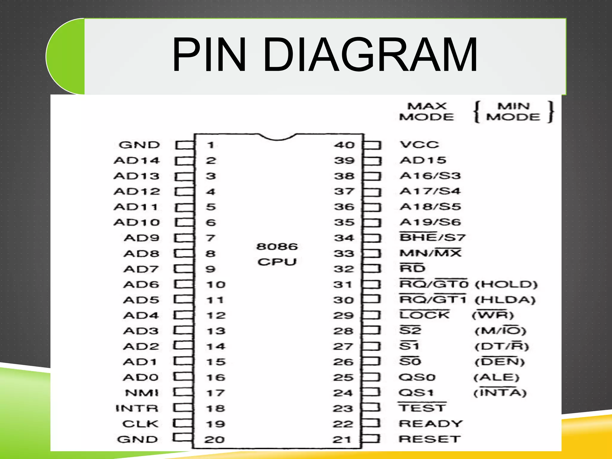
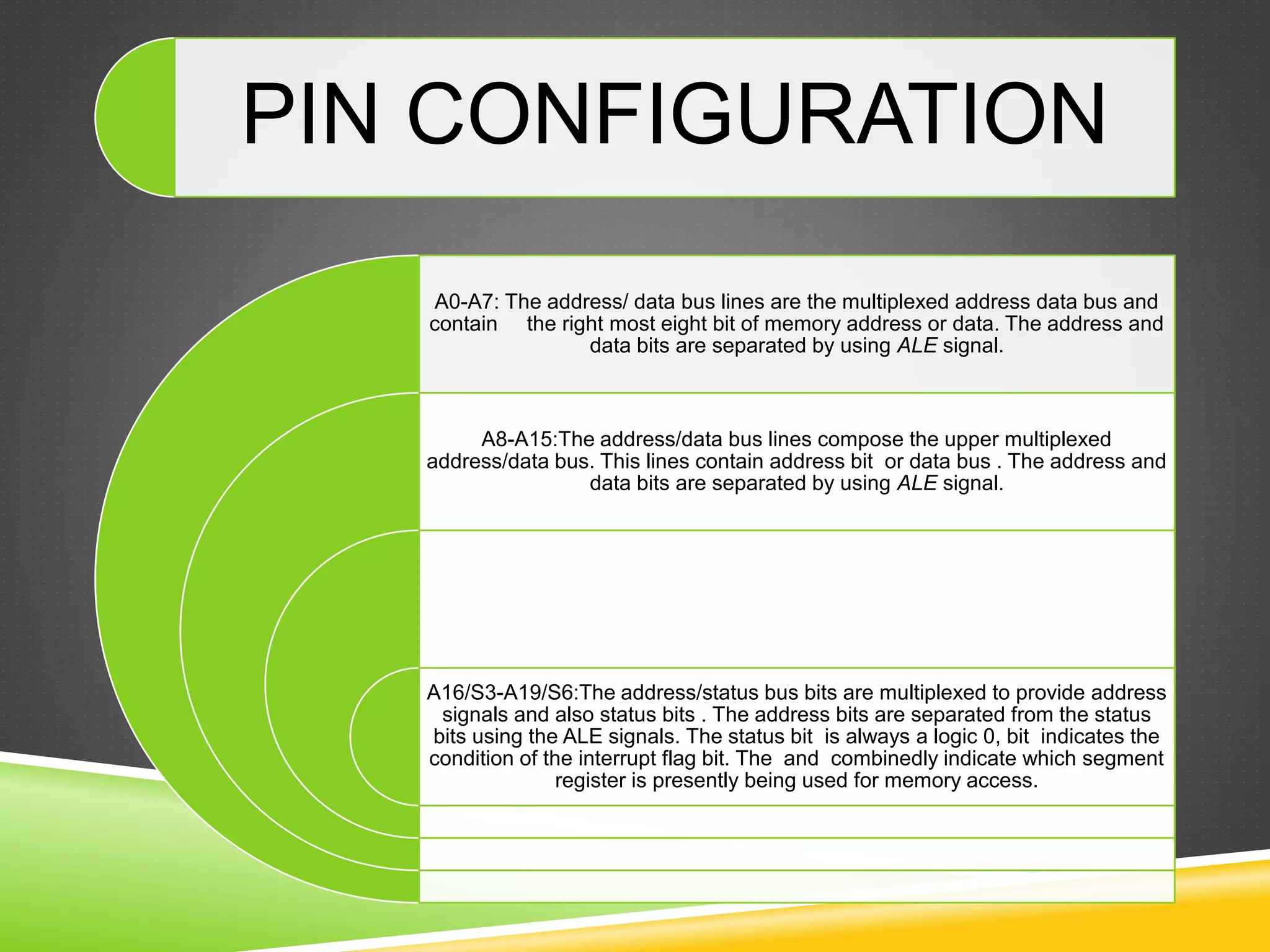
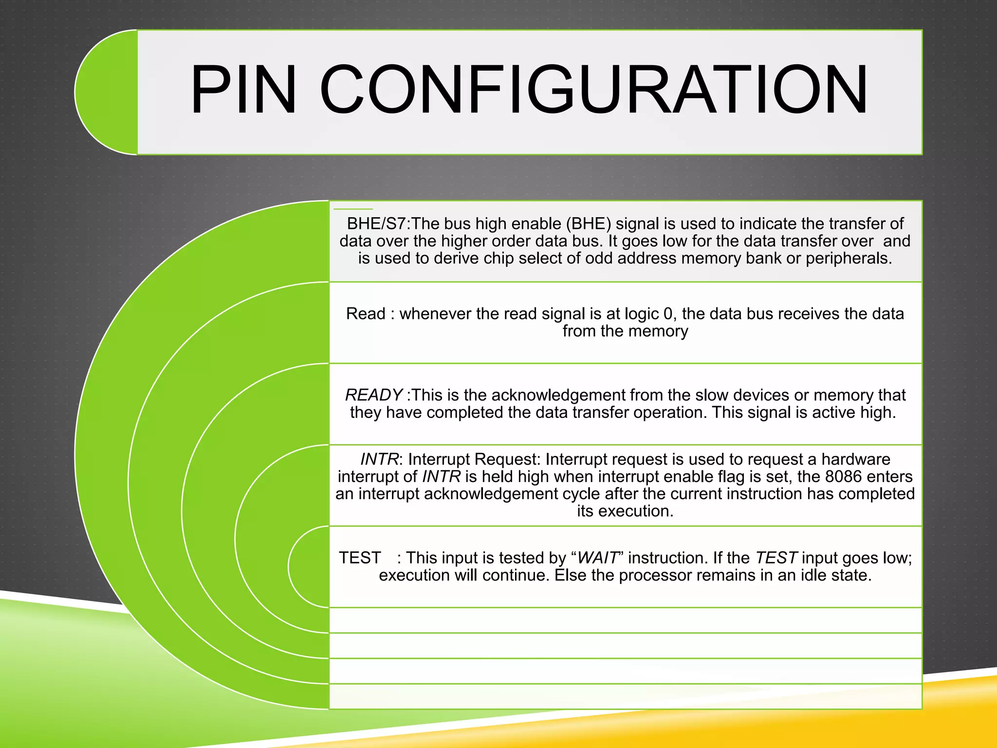
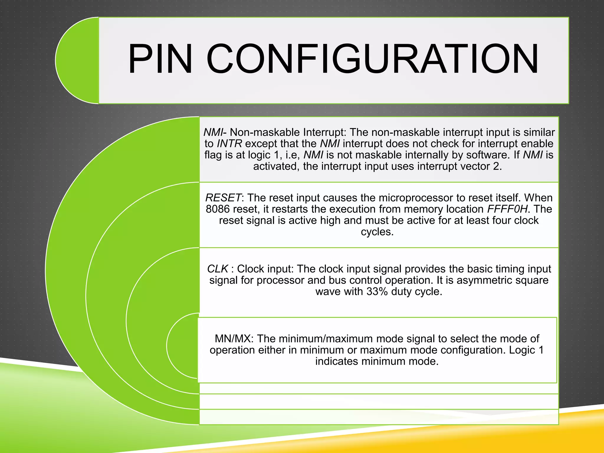
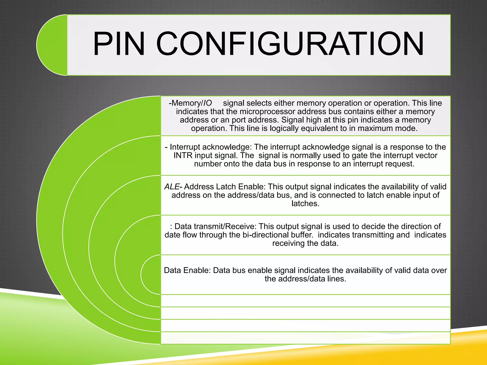
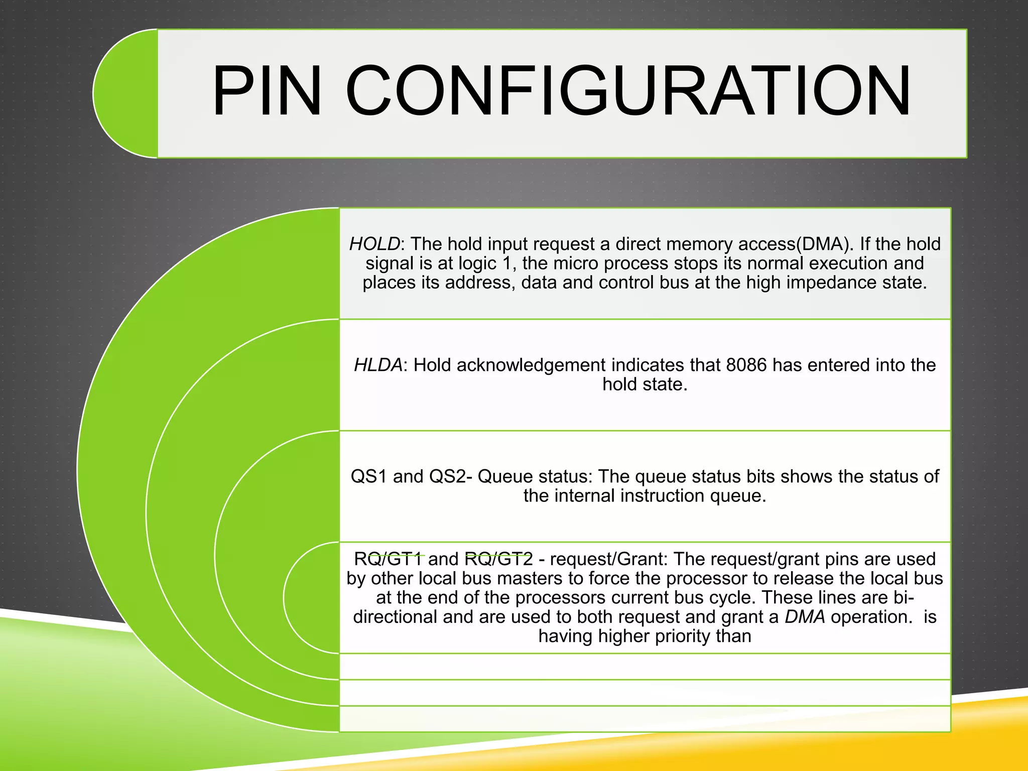


This document provides a pin diagram and configuration for an NRI Institute of Research Science and Technology chip. It describes the functions of pins including the address/data bus, status bits, interrupt request lines, clock input, memory/IO selection, and direct memory access control lines like HOLD and HLDA. The pin configuration section defines over 20 input and output pins for memory addressing, interrupt handling, bus control and chip interfacing.