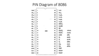
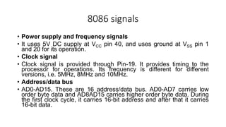
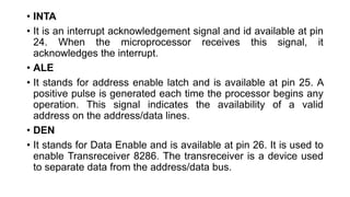
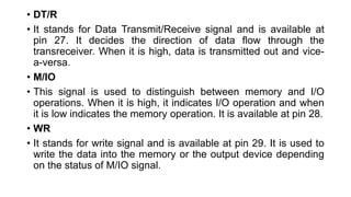
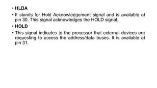
The 8086 has several pins and signals that facilitate its operation and communication with external devices:
- It uses a 5V DC power supply and clock signal for timing. The address/data and address/status buses are used to transmit addresses and data.
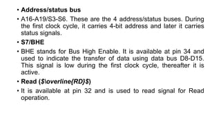
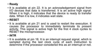
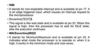
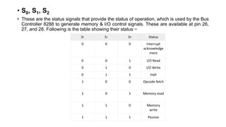
- Additional control signals include READ, READY, RESET, INTR, NMI, TEST, MN/MX, INTA, ALE, DEN, DT/R, M/IO, WR, HLDA, HOLD, QS1, QS0, S0-S2, and LOCK to manage interrupts, I/O, memory access, and bus control.
- The status pins QS1, QS0 and S0-S


![[Deck] What's New in Spark-Iceberg Integration via DSV2.pptx](https://cdn.slidesharecdn.com/ss_thumbnails/deckwhatsnewinspark-icebergintegrationviadsv2-260210005337-25955b12-thumbnail.jpg?width=640&height=640&fit=bounds)


