SlideShare a Scribd company logo
1 of 61
Basic Electronics
Course content
1. Semiconductor basics
Diode Theory
2. The PN Junction Diode Characteristics
3. Forward and Reverse Biased PN Junction
4. Diode applications
Transistor Theory
1. Bipolar NPN Transistor Construction
2. NPN Transistor Principle
3. Transistor Configurations
4. DC Operating Conditions
5. Transistors Applications
6. Other types of transistors
Digital Basics
1. Binary numbers
2. Basic Logic Gates
3. Basic Digital Circuits
Diode Theory
Semi-conductors materials such as Silicon and
Germanium, have electrical properties somewhere in the
middle, between those of a "Conductor" and an
"Insulator". They are not good conductors nor good
insulators (hence their name semi-conductors). They
have very few "free electrons" .
Semiconductor Basics
Silicon and Germanium atom ability to conduct electricity
can be greatly improved by adding certain "Impurities" to
this crystalline structure thereby, producing more free
electrons than holes or vice versa.
Silicon Atom & Crystal Lattice
N-Type Semiconductor
In order for our silicon crystal to conduct electricity, we need to
introduce an impurity atom such as Arsenic, Antimony or
Phosphorus into the crystalline structure. These atoms have five
outer electrons in their outermost shell or orbit. This crystalline
structure is called N-Type Semiconductor.
P-Type Semiconductor
To have a P-type semiconductor , we need to introduce an impurity
atom such as Boron, Aluminium ,or Indium into the crystalline
structure. These atoms have Three outer electrons in their outermost
shell or orbit. This crystalline structure is called P-Type Semiconductor
PN Junction Diode Characteristics
By manufacturing a component which will have N-Type
semiconductor structure in one side and P-Type
semiconductor in other side a PN Junction Diode is
formed. P-Type semiconductor N-Type semiconductor
P-N Junction
Diode I, V curve
Applying a forward bias voltage i.e. the p-type connection to battery
(+), this region can be made to contract, thereby taking on a forward
resistance of only a few ohms. This enables a high current to flow. Apply
the battery in the opposite direction as a reverse bias and the junction
expands forming an extremely high resistance.
Forward Biased PN Junction
When connecting the battery +V to the
p-type material the junction is said to be
Forward biased. Negative electrons will
cross to the p-region attracted by the
battery (+) potential and positive holes will
move into the n-region, similarly attracted
by the negative battery potential.
It takes a potential of about 0.6V to
overcome the junction barrier of a silicon
diode, (germanium types require less at
approximately 0.25V), than large current
flow in the junction due to small value of
junction Resistance.
Reverse Biased PN Junction
When connecting the battery +V the
opposite direction, i.e connecting
+V to N-type material, the junction
will be called Reversed biased. In
reverse bias the PN Junction will
expand, making the junction have high
resistance. A reverse biased junction
can develop a resistance of many
millions of Ohms.
If Voltage increases up to 50V a
dramatic increase in current will
occur , due to the much lower diode
resistance.
Diode Symbols & Real component
Simple Diode Circuit in Forward Bias
Simple Diode Circuit in Reverse Bias
Diode Multimeter Check
Connected this
way across the
diode, the meter
should show a very
low resistance
Connected the
other way across
the diode, it should
show a very high
resistance.
Diode function Multimeter Check
special “diode check”
function which
displays the actual
forward voltage drop
of the diode in volts.
Diode Applications
Diode as a Rectifier
Rectification is the conversion of alternating current (AC) to direct current (DC).
The simplest kind of rectifier circuit is the half-wave rectifier. It only allows one
half of an AC waveform to pass through to the load.
Diode Applications………………….. continues
LED (Light Emitting Diode)
The Light Emitting Diode LED, is a PN junction diode that
will emit light when forward biased, that is when current
flows from its anode to the cathode.
The forward voltage drop can be between 1.6V and 2V
depending upon the device type.
Here is an LED Example
Diode Applications………………….. continues
Seven Segment Light Emitting Diode
Light emitting diodes can be connected together as an array .
Seven segment' device frequently found as part of a numerical display.
These devices produce a bright visual indicator with a number count from 0
to 9 and usually include a decimal point.
Transistor Theory
Bipolar NPN Transistor Construction
There are two bipolar transistor types, NPN and PNP.
The operating conditions are considered for the more popular NPN type,
which consists of two PN junctions fused together to form one continuous
piece of semiconductor material, with the connections as shown.
NPN Transistor construction can be represented as two back-to-back diodes.
Bipolar NPN Transistor symbol & Real component
Transistor Theory ……… continues
Transistor Theory
NPN Transistor Principle
IB
IC
IE
IE = IC + IB
IC = IE - IB
IB = IE - IC
Typical IB = 2% IE
Hence IC = 98% IE
Current Gain,β, hFE = IC/IB
In this example, β, hFE = 50
hFE value will be found in transistor data books, and will vary between different transistor types and is determined during manufacture.
Transistor Configurations
Three main connection configurations for a transistor.
Each has a particular purpose.
The 'common emitter' will
have a medium input and
output impedance
measured in Kilo Ohms.
First One
Second
The 'common base'
configuration has a
gain of less than 1.
The input impedance
is low and output
high making it ideal
as a matching circuit.
The 'common
collector' or 'emitter
follower' has a high
input impedance and
low output.
Third
Transistor Applications
Transistor as a Switch :
When used as a current switch the transistor will be forced to operate in
either of two states. Fully ON and conducting the maximum collecter
current or OFF where ideally no current flows at all.
Simple Signal Amplifier :
The common emitter transistor will amplify the small input AC voltage,
thereby causing collector current to flow in R2. The output voltage change
(input volts × Av) is as a result of the alternating collector current in R2.
The output signal voltage is at 180° phase inversion to that at the input.
Other types of Transistors
Field Effect Transistor, FET :
Bipolar Junction Transistors, BJT are CURRENT operated device,
on other hand The Field Effect Transistor, or simply FET however, use
the voltage that is applied to their input terminal to control the output
current, since their operation relies on the electric field (hence the name
field effect) generated by the input voltage. This then makes the Field
Effect Transistor a VOLTAGE operated device.
Bipolar Transistor
Field Effect
Transistor
Emitter - (E) Source - (S)
Base - (B) Gate - (G)
Collector - (C) Drain - (D)
FET’s symbols :
MOSFET’s symbols :
MOSFET stand for Metal Oxide Semiconductor Field Effect Transistor.
Digital Basics
Binary numbers :
What is Decimal, Binary, Hexadecimal,
Octal numbers ?
Decimal :
We count numbers in what is called the decimal
number system. Decimal has 10 digits which are
0,1,2,3,4,5,6,7,8,9. Decimal is also called base 10
because it has 10 digits. The reason why people
started counting in decimal is because it has 10
digits and we have 10 fingers and people used to use
their fingers for counting.
Example of Decimal Numbers :
1. 2310 2. 5410
Binary numbering system uses only 2 digits
which are 0 and 1 and is also called base 2.
Binary is what computers use for counting
because inside a computer you get things that
are like little switches that can be either off or
on(0 or 1).
Example of Binary Numbers :
1. 10012 2. 10110012
Binary :
Hexadecimal :
The word hexadecimal is made up of 2 parts which are
hex(6) and decimal(10). If you add 6 and 10 together
you get 16 and that is how many digits there are in
hexadecimal. Hexadecimal is sometimes called hex or
base 16. To get 16 digits we have to use letters of the
alphabet and those 16 digits are
0,1,2,3,4,5,6,7,8,9,A,B,C,D,E,F. Hexadecimal is often
used instead of binary
Example of Hexadecimal Numbers :
1. 3FF16 2. AB316
Octal uses 8 digits which are 0,1,2,3,4,5,6,7 and
is also called base 8. We use a subscripted 8 to
show that a number is octal.
Example of Octal Numbers :
1. 2758 2. 1238
Octal :
Binary numbers analysis :
MSB LSB
2 2 2 2 2 2 ³ 2² 2¹ 2º
256 128 64 32 16 8 4 2 1
6 58 7 4
2nd
Digit 1st
Digit3rd
Digit7th
Digit 6th
Digit8th
Digit 3rd
Digit5th
Digit
4th
Digit
Most Significant Bit Least Significant Bit
Decimal to Binary conversion :
Example-1
Convert the decimal number 3410 to Binary?
Solution:
Considering the table for Binary number analysis
, the Binary number will be equal to 1000102.
Example-2
Convert the decimal number 24510 to Binary?
Solution:
Considering the table for Binary number analysis
, the Binary number will be equal to 111101012.
Example-3
Convert the decimal number 510 to Binary?
Solution:
Considering the table for Binary number analysis
, the Binary number will be equal to 1012.
Convert the decimal number 134610 to Binary?
Solution:
Considering the table for Binary number analysis
, the Binary number will be equal to 101010000102.
Example-4
Binary to Decimal conversion :
Example-1
Convert the Binary number 11112 to Decimal?
Solution:
Considering the table for Binary number analysis
, the Decimal number will be equal to 1510.
Example-2
Convert the Binary number 11001012 to Decimal?
Solution:
Considering the table for Binary number analysis
, the Decimal number will be equal to 10110.
Example-3
Convert the Binary number 10012 to Decimal?
Solution:
Considering the table for Binary number analysis
, the Decimal number will be equal to 910.
Convert the Binary number 111112 to Decimal?
Solution:
Considering the table for Binary number analysis
, the Decimal number will be equal to 3110.
Example-4
Hexadecimal to Binary conversion :
Example-1
Convert the Hexadecimal number 1F116 to Binary?
Solution:
Note that, each Hexadecimal digit can be considered to
have four sub-digits.
Hence the above Hexadecimal digit can be arranged as
below
1 F 1
0001 1111 0001
Hence the Binary number equal to 1111100012.
Hexadecimal
Convert the Hexadecimal number FFFA16 to Binary?
Solution:
Note that, each Hexadecimal digit can be considered to
have four sub-digits.
Hence the above Hexadecimal digit can be arranged as
below
Example-2
F F F A
1111 1111 1111 1010
Hence the Binary number equal to 11111111111110102.
Binary to Hexadecimal conversion :
Example-1
Convert the Binary number 1010102 to Hexadecimal?
Solution:
Hence the Hexadecimal digit is equal 2A16.
0010 1010
2 A Hexadecimal
Binary
Example-2
Convert the Binary number 111110102 to Hexadecimal?
Solution:
Hence the Hexadecimal digit is equal FA16.
1111 1010
F A
Hexadecimal to Decimal conversion :
In this type of conversion , you first convert your
hexadecimal number to Binary, then convert binary
to Decimal.
For Octal conversion to Binary or
Hexadecimal :
Each octal digit can be converted to three sub-digits,
similar to the hexadecimal system conversion.
Basic Logic Gates
Digital systems are said to be
constructed by using logic gates. These
gates are the AND, OR, NOT, NAND,
NOR, EXOR and EXNOR gates. The
basic operations are described below
with the aid of Truth Tables
Logic gates :
The AND gate is an electronic circuit that gives a
high output (1) only if all its inputs are high.
A dot (.) is used to show the AND operation
i.e. A.B. Bear in mind that this dot is sometimes
omitted i.e. AB
AND gate
OR gate
The OR gate is an electronic circuit that gives a
high output (1) if one or more of its inputs are high.
A plus (+) is used to show the OR operation.
NOT gate
The NOT gate is an electronic circuit that produces
an inverted version of the input at its output. It is
also known as an inverter. If the input variable is A,
the inverted output is known as NOT A. This is also
shown as A', or A with a bar over the top, as shown at
the outputs. The diagrams below show two ways that
the NAND logic gate can be configured to produce a
NOT gate. It can also be done using NOR logic gates
in the same way.
NAND gate
This is a NOT-AND gate which is equal to an AND gate
followed by a NOT gate. The outputs of all NAND gates
are high if any of the inputs are low. The symbol is an
AND gate with a small circle on the output. The small
circle represents inversion.
NOR gate
This is a NOT-OR gate which is equal to an OR gate
followed by a NOT gate. The outputs of all NOR
gates are low if any of the inputs are high.
The symbol is an OR gate with a small circle on the
output. The small circle represents inversion
EXOR gate
The 'Exclusive-OR' gate is a circuit which will give a
high output if either, but not both, of its two inputs
are high. An encircled plus sign is used to show
the EXOR operation
+
EXNOR gate
The 'Exclusive-NOR' gate circuit does the opposite to
the EOR gate. It will give a low output if either, but not
both, of its two inputs are high. The symbol is an EXOR
gate with a small circle on the output. The small circle
represents inversion.
The NAND and NOR gates are called universal functions
since with either one the AND and OR functions and NOT
can be generated.
A function in sum of products form can be implemented
using NAND gates by replacing all AND and OR gates by
NAND gates.
A function in product of sums form can be implemented
using NOR gates by replacing
Gates symbol summary
Basic Digital Circuits
There are basically two kinds of digital circuits, created
from connected gates:
1. Combinational circuits : Which are formed by using the
output of one gate as the input of another gate.
2. Sequential Logic circuits: The outputs of the circuit
"fed back" as inputs to the circuit.
Digital Circuit design (at least for simple circuits) is
accomplished by developing a truth table that describe
the input and output of the circuit, then deriving the
simplest Boolean statements that satisfy the table
and, finally, drawing the digital circuit that represents
the Boolean statements.
Digital Circuits as MEMORY:
The basic gates can be used to construct digital circuits that
store digital data, 0 or 1, they can be retained until inputs reset
them. The latch is the simplest circuit that can store and retain
one of two values; when applied to digital circuits, this means
that a simple latch can store One bit. (In fact there are complex
latches that can store more than one bit.) . A latch has a data
input, a clock input and an output. When the clock input is
active, data on the input is "latched" or stored and transfered to
the output either immediately or when the clock input goes
inactive. The output will then retain its value until the clock goes
active again. However, the latch has some shortcomings and
non intuitive characteristics, so it is not the basic element for
computer storage.
The flip-flop is the fundamental circuit used to construct
storage units. A digital logic circuit that can be in one of two
states which it switches (or "toggles") between under control of
its inputs. It can thus be considered as a one bit memory. Three
types of flip-flop are common: the SR flip-flop, the JK flip-flop
and the D-type flip-flop (or latch).
S-R Latch :
It is also called the "RS latch", using it to illustrate how
gate circuits can "store" digital data. The S-R latch, one
of the simplest sequential circuits, is made up of paired
NAND gates.
The outputs ,Q and Q' in are
complements of one another. Both
are available as outputs to other
circuits, but, when used for
storage, Q gives the value of the
bit represented by the latch.
Shortcomings of the S-R latch to become a storage unit
Clocked RS NAND Latch
By adding a pair of NAND gates to the input circuits of the RS latch ,
a clocked RS latch is built
The clocked RS latch solves
some of the problems of basic
RS latch circuit, and allows
closer control of the latching
action. However, it is by no
means a complete solution.
The clocked RS latch solves some of the problems of basic RS latch circuit,
and allows closer control of the latching action. However, it is by no means a
complete solution.
The Edge-Triggered RS Flip-Flop
To adjust the clocked RS latch for edge triggering, we must actually combine
two identical clocked latch circuits, but have them operate on opposite
halves of the clock signal. The resulting circuit is commonly called a flip-flop,
because its output can first flip one way and then flop back the other way.
The clocked RS latch is also sometimes called a flip-flop, although it is more
properly referred to as a latch circuit.

More Related Content

What's hot

What's hot (20)

Introduction to Basic Electronics
Introduction to Basic ElectronicsIntroduction to Basic Electronics
Introduction to Basic Electronics
 
Introduction to active and passive components
Introduction to active and passive components Introduction to active and passive components
Introduction to active and passive components
 
Semiconductor Devices
Semiconductor DevicesSemiconductor Devices
Semiconductor Devices
 
Ge 2151 basic electrical electronics engineering
Ge 2151 basic electrical electronics engineering Ge 2151 basic electrical electronics engineering
Ge 2151 basic electrical electronics engineering
 
Electrical energy meter
Electrical energy meterElectrical energy meter
Electrical energy meter
 
Function generator
Function generatorFunction generator
Function generator
 
digita storage oscilloscope (dso)
digita storage oscilloscope (dso)digita storage oscilloscope (dso)
digita storage oscilloscope (dso)
 
BASIC ELECTRONICS!!
BASIC ELECTRONICS!!BASIC ELECTRONICS!!
BASIC ELECTRONICS!!
 
Basic electronics
Basic electronics Basic electronics
Basic electronics
 
Electronic Measurement and Instrumentation
Electronic Measurement and InstrumentationElectronic Measurement and Instrumentation
Electronic Measurement and Instrumentation
 
Transistor
TransistorTransistor
Transistor
 
3.bipolar junction transistor (bjt)
3.bipolar junction transistor (bjt)3.bipolar junction transistor (bjt)
3.bipolar junction transistor (bjt)
 
Inductors
InductorsInductors
Inductors
 
Semiconductor devices
Semiconductor devicesSemiconductor devices
Semiconductor devices
 
Transistor basics
Transistor   basicsTransistor   basics
Transistor basics
 
Diodes basics
Diodes   basicsDiodes   basics
Diodes basics
 
Diodes and Its Application
Diodes and Its ApplicationDiodes and Its Application
Diodes and Its Application
 
Introduction to electronics - Third session
Introduction to electronics - Third sessionIntroduction to electronics - Third session
Introduction to electronics - Third session
 
Evolution of electronics
Evolution of electronicsEvolution of electronics
Evolution of electronics
 
Electronics Introduction
Electronics IntroductionElectronics Introduction
Electronics Introduction
 

Similar to basic electronics

Simple 100 w inverter circuit
Simple 100 w inverter circuitSimple 100 w inverter circuit
Simple 100 w inverter circuitNarasimha Reddy
 
Basic Electronics
Basic Electronics Basic Electronics
Basic Electronics Omkar Rane
 
Basi electroni components lecture
Basi electroni components lectureBasi electroni components lecture
Basi electroni components lectureCherehaniMakigo
 
basic-analog-electronics
basic-analog-electronicsbasic-analog-electronics
basic-analog-electronicsATTO RATHORE
 
Physics investigatory projec tdocx
Physics investigatory projec tdocxPhysics investigatory projec tdocx
Physics investigatory projec tdocxHrithiksingla
 
IJSRED-V2I2P61
IJSRED-V2I2P61IJSRED-V2I2P61
IJSRED-V2I2P61IJSRED
 
Electronics ckts symbols
Electronics ckts symbolsElectronics ckts symbols
Electronics ckts symbolsmanish katara
 
EC8252 NOTES 3rd to 5th unit_compressed.pdf
EC8252 NOTES 3rd to 5th unit_compressed.pdfEC8252 NOTES 3rd to 5th unit_compressed.pdf
EC8252 NOTES 3rd to 5th unit_compressed.pdfkabileshsk2
 
Electricity and Electronic
Electricity and ElectronicElectricity and Electronic
Electricity and ElectronicXosé Rodríguez
 
EEE Unit III first year. .pptx
EEE Unit III first year.           .pptxEEE Unit III first year.           .pptx
EEE Unit III first year. .pptxsrujan0444
 
1 100 transistorcircuits
1 100 transistorcircuits1 100 transistorcircuits
1 100 transistorcircuitsAlejandro Perez
 
Type of pn junction & rectifiers plus Transistor
Type of pn junction & rectifiers plus TransistorType of pn junction & rectifiers plus Transistor
Type of pn junction & rectifiers plus TransistorMuhammad Adeel Shakir
 
Transistors what are_they
Transistors what are_theyTransistors what are_they
Transistors what are_theyprasadpawaskar
 
Pre Final Year project/ mini project for Electronics and communication engine...
Pre Final Year project/ mini project for Electronics and communication engine...Pre Final Year project/ mini project for Electronics and communication engine...
Pre Final Year project/ mini project for Electronics and communication engine...Shirshendu Das
 

Similar to basic electronics (20)

9. transistors.rr
9. transistors.rr9. transistors.rr
9. transistors.rr
 
9. transistors.rr
9. transistors.rr9. transistors.rr
9. transistors.rr
 
ELECTRONICS
ELECTRONICSELECTRONICS
ELECTRONICS
 
Simple 100 w inverter circuit
Simple 100 w inverter circuitSimple 100 w inverter circuit
Simple 100 w inverter circuit
 
Basic Electronics
Basic Electronics Basic Electronics
Basic Electronics
 
Basi electroni components lecture
Basi electroni components lectureBasi electroni components lecture
Basi electroni components lecture
 
basic-analog-electronics
basic-analog-electronicsbasic-analog-electronics
basic-analog-electronics
 
Physics investigatory projec tdocx
Physics investigatory projec tdocxPhysics investigatory projec tdocx
Physics investigatory projec tdocx
 
IJSRED-V2I2P61
IJSRED-V2I2P61IJSRED-V2I2P61
IJSRED-V2I2P61
 
Electronics ckts symbols
Electronics ckts symbolsElectronics ckts symbols
Electronics ckts symbols
 
Cro ppt
Cro pptCro ppt
Cro ppt
 
Edcqnaunit 8
Edcqnaunit 8Edcqnaunit 8
Edcqnaunit 8
 
EC8252 NOTES 3rd to 5th unit_compressed.pdf
EC8252 NOTES 3rd to 5th unit_compressed.pdfEC8252 NOTES 3rd to 5th unit_compressed.pdf
EC8252 NOTES 3rd to 5th unit_compressed.pdf
 
Electricity and Electronic
Electricity and ElectronicElectricity and Electronic
Electricity and Electronic
 
EEE Unit III first year. .pptx
EEE Unit III first year.           .pptxEEE Unit III first year.           .pptx
EEE Unit III first year. .pptx
 
1 100 transistorcircuits
1 100 transistorcircuits1 100 transistorcircuits
1 100 transistorcircuits
 
Type of pn junction & rectifiers plus Transistor
Type of pn junction & rectifiers plus TransistorType of pn junction & rectifiers plus Transistor
Type of pn junction & rectifiers plus Transistor
 
Transistors what are_they
Transistors what are_theyTransistors what are_they
Transistors what are_they
 
Ch03updated
Ch03updatedCh03updated
Ch03updated
 
Pre Final Year project/ mini project for Electronics and communication engine...
Pre Final Year project/ mini project for Electronics and communication engine...Pre Final Year project/ mini project for Electronics and communication engine...
Pre Final Year project/ mini project for Electronics and communication engine...
 

More from ATTO RATHORE

8085-microprocessor
8085-microprocessor8085-microprocessor
8085-microprocessorATTO RATHORE
 
8085-microprocessor
8085-microprocessor8085-microprocessor
8085-microprocessorATTO RATHORE
 
bharat-electronics-limited
bharat-electronics-limitedbharat-electronics-limited
bharat-electronics-limitedATTO RATHORE
 
bharat-electonics-limited
 bharat-electonics-limited bharat-electonics-limited
bharat-electonics-limitedATTO RATHORE
 
industrial-training-in-bharat-electronics-limited
 industrial-training-in-bharat-electronics-limited industrial-training-in-bharat-electronics-limited
industrial-training-in-bharat-electronics-limitedATTO RATHORE
 
bharat-electronics-limited-ppt
bharat-electronics-limited-pptbharat-electronics-limited-ppt
bharat-electronics-limited-pptATTO RATHORE
 
bharat-eectronics-limited-a-study-on-working-of-different-department
bharat-eectronics-limited-a-study-on-working-of-different-departmentbharat-eectronics-limited-a-study-on-working-of-different-department
bharat-eectronics-limited-a-study-on-working-of-different-departmentATTO RATHORE
 
transmission-line-and-waveguide-ppt
transmission-line-and-waveguide-ppttransmission-line-and-waveguide-ppt
transmission-line-and-waveguide-pptATTO RATHORE
 

More from ATTO RATHORE (20)

8085-microprocessor
8085-microprocessor8085-microprocessor
8085-microprocessor
 
microprocessor
 microprocessor microprocessor
microprocessor
 
8085-microprocessor
8085-microprocessor8085-microprocessor
8085-microprocessor
 
microprocessor
   microprocessor   microprocessor
microprocessor
 
bel-ppt-pptx
bel-ppt-pptxbel-ppt-pptx
bel-ppt-pptx
 
bharat-electronics-limited
bharat-electronics-limitedbharat-electronics-limited
bharat-electronics-limited
 
bel-radar
bel-radarbel-radar
bel-radar
 
bharat-electonics-limited
 bharat-electonics-limited bharat-electonics-limited
bharat-electonics-limited
 
industrial-training-in-bharat-electronics-limited
 industrial-training-in-bharat-electronics-limited industrial-training-in-bharat-electronics-limited
industrial-training-in-bharat-electronics-limited
 
bharat-electronics-limited-ppt
bharat-electronics-limited-pptbharat-electronics-limited-ppt
bharat-electronics-limited-ppt
 
bharat-eectronics-limited-a-study-on-working-of-different-department
bharat-eectronics-limited-a-study-on-working-of-different-departmentbharat-eectronics-limited-a-study-on-working-of-different-department
bharat-eectronics-limited-a-study-on-working-of-different-department
 
basic electronics
basic    electronicsbasic    electronics
basic electronics
 
basic electronics
basic   electronicsbasic   electronics
basic electronics
 
basic-electronics
basic-electronicsbasic-electronics
basic-electronics
 
basic-electronics
basic-electronicsbasic-electronics
basic-electronics
 
transmission-line-and-waveguide-ppt
transmission-line-and-waveguide-ppttransmission-line-and-waveguide-ppt
transmission-line-and-waveguide-ppt
 
waveguide-1
waveguide-1waveguide-1
waveguide-1
 
waveguides-ppt
waveguides-pptwaveguides-ppt
waveguides-ppt
 
ppt-of-waveguide
ppt-of-waveguideppt-of-waveguide
ppt-of-waveguide
 
wave-guides
wave-guideswave-guides
wave-guides
 

Recently uploaded

GDSC ASEB Gen AI study jams presentation
GDSC ASEB Gen AI study jams presentationGDSC ASEB Gen AI study jams presentation
GDSC ASEB Gen AI study jams presentationGDSCAESB
 
Past, Present and Future of Generative AI
Past, Present and Future of Generative AIPast, Present and Future of Generative AI
Past, Present and Future of Generative AIabhishek36461
 
Study on Air-Water & Water-Water Heat Exchange in a Finned Tube Exchanger
Study on Air-Water & Water-Water Heat Exchange in a Finned Tube ExchangerStudy on Air-Water & Water-Water Heat Exchange in a Finned Tube Exchanger
Study on Air-Water & Water-Water Heat Exchange in a Finned Tube ExchangerAnamika Sarkar
 
SPICE PARK APR2024 ( 6,793 SPICE Models )
SPICE PARK APR2024 ( 6,793 SPICE Models )SPICE PARK APR2024 ( 6,793 SPICE Models )
SPICE PARK APR2024 ( 6,793 SPICE Models )Tsuyoshi Horigome
 
Churning of Butter, Factors affecting .
Churning of Butter, Factors affecting  .Churning of Butter, Factors affecting  .
Churning of Butter, Factors affecting .Satyam Kumar
 
Decoding Kotlin - Your guide to solving the mysterious in Kotlin.pptx
Decoding Kotlin - Your guide to solving the mysterious in Kotlin.pptxDecoding Kotlin - Your guide to solving the mysterious in Kotlin.pptx
Decoding Kotlin - Your guide to solving the mysterious in Kotlin.pptxJoão Esperancinha
 
Software and Systems Engineering Standards: Verification and Validation of Sy...
Software and Systems Engineering Standards: Verification and Validation of Sy...Software and Systems Engineering Standards: Verification and Validation of Sy...
Software and Systems Engineering Standards: Verification and Validation of Sy...VICTOR MAESTRE RAMIREZ
 
What are the advantages and disadvantages of membrane structures.pptx
What are the advantages and disadvantages of membrane structures.pptxWhat are the advantages and disadvantages of membrane structures.pptx
What are the advantages and disadvantages of membrane structures.pptxwendy cai
 
chaitra-1.pptx fake news detection using machine learning
chaitra-1.pptx  fake news detection using machine learningchaitra-1.pptx  fake news detection using machine learning
chaitra-1.pptx fake news detection using machine learningmisbanausheenparvam
 
main PPT.pptx of girls hostel security using rfid
main PPT.pptx of girls hostel security using rfidmain PPT.pptx of girls hostel security using rfid
main PPT.pptx of girls hostel security using rfidNikhilNagaraju
 
Electronically Controlled suspensions system .pdf
Electronically Controlled suspensions system .pdfElectronically Controlled suspensions system .pdf
Electronically Controlled suspensions system .pdfme23b1001
 
Gurgaon ✡️9711147426✨Call In girls Gurgaon Sector 51 escort service
Gurgaon ✡️9711147426✨Call In girls Gurgaon Sector 51 escort serviceGurgaon ✡️9711147426✨Call In girls Gurgaon Sector 51 escort service
Gurgaon ✡️9711147426✨Call In girls Gurgaon Sector 51 escort servicejennyeacort
 
power system scada applications and uses
power system scada applications and usespower system scada applications and uses
power system scada applications and usesDevarapalliHaritha
 
OSVC_Meta-Data based Simulation Automation to overcome Verification Challenge...
OSVC_Meta-Data based Simulation Automation to overcome Verification Challenge...OSVC_Meta-Data based Simulation Automation to overcome Verification Challenge...
OSVC_Meta-Data based Simulation Automation to overcome Verification Challenge...Soham Mondal
 
HARMONY IN THE NATURE AND EXISTENCE - Unit-IV
HARMONY IN THE NATURE AND EXISTENCE - Unit-IVHARMONY IN THE NATURE AND EXISTENCE - Unit-IV
HARMONY IN THE NATURE AND EXISTENCE - Unit-IVRajaP95
 
Architect Hassan Khalil Portfolio for 2024
Architect Hassan Khalil Portfolio for 2024Architect Hassan Khalil Portfolio for 2024
Architect Hassan Khalil Portfolio for 2024hassan khalil
 
Biology for Computer Engineers Course Handout.pptx
Biology for Computer Engineers Course Handout.pptxBiology for Computer Engineers Course Handout.pptx
Biology for Computer Engineers Course Handout.pptxDeepakSakkari2
 

Recently uploaded (20)
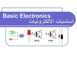
★ CALL US 9953330565 ( HOT Young Call Girls In Badarpur delhi NCR
★ CALL US 9953330565 ( HOT Young Call Girls In Badarpur delhi NCR★ CALL US 9953330565 ( HOT Young Call Girls In Badarpur delhi NCR
★ CALL US 9953330565 ( HOT Young Call Girls In Badarpur delhi NCR
 
GDSC ASEB Gen AI study jams presentation
GDSC ASEB Gen AI study jams presentationGDSC ASEB Gen AI study jams presentation
GDSC ASEB Gen AI study jams presentation
 
Past, Present and Future of Generative AI
Past, Present and Future of Generative AIPast, Present and Future of Generative AI
Past, Present and Future of Generative AI
 
Study on Air-Water & Water-Water Heat Exchange in a Finned Tube Exchanger
Study on Air-Water & Water-Water Heat Exchange in a Finned Tube ExchangerStudy on Air-Water & Water-Water Heat Exchange in a Finned Tube Exchanger
Study on Air-Water & Water-Water Heat Exchange in a Finned Tube Exchanger
 
SPICE PARK APR2024 ( 6,793 SPICE Models )
SPICE PARK APR2024 ( 6,793 SPICE Models )SPICE PARK APR2024 ( 6,793 SPICE Models )
SPICE PARK APR2024 ( 6,793 SPICE Models )
 
Churning of Butter, Factors affecting .
Churning of Butter, Factors affecting  .Churning of Butter, Factors affecting  .
Churning of Butter, Factors affecting .
 
Decoding Kotlin - Your guide to solving the mysterious in Kotlin.pptx
Decoding Kotlin - Your guide to solving the mysterious in Kotlin.pptxDecoding Kotlin - Your guide to solving the mysterious in Kotlin.pptx
Decoding Kotlin - Your guide to solving the mysterious in Kotlin.pptx
 
Software and Systems Engineering Standards: Verification and Validation of Sy...
Software and Systems Engineering Standards: Verification and Validation of Sy...Software and Systems Engineering Standards: Verification and Validation of Sy...
Software and Systems Engineering Standards: Verification and Validation of Sy...
 
What are the advantages and disadvantages of membrane structures.pptx
What are the advantages and disadvantages of membrane structures.pptxWhat are the advantages and disadvantages of membrane structures.pptx
What are the advantages and disadvantages of membrane structures.pptx
 
chaitra-1.pptx fake news detection using machine learning
chaitra-1.pptx  fake news detection using machine learningchaitra-1.pptx  fake news detection using machine learning
chaitra-1.pptx fake news detection using machine learning
 
main PPT.pptx of girls hostel security using rfid
main PPT.pptx of girls hostel security using rfidmain PPT.pptx of girls hostel security using rfid
main PPT.pptx of girls hostel security using rfid
 
Electronically Controlled suspensions system .pdf
Electronically Controlled suspensions system .pdfElectronically Controlled suspensions system .pdf
Electronically Controlled suspensions system .pdf
 
Gurgaon ✡️9711147426✨Call In girls Gurgaon Sector 51 escort service
Gurgaon ✡️9711147426✨Call In girls Gurgaon Sector 51 escort serviceGurgaon ✡️9711147426✨Call In girls Gurgaon Sector 51 escort service
Gurgaon ✡️9711147426✨Call In girls Gurgaon Sector 51 escort service
 
POWER SYSTEMS-1 Complete notes examples
POWER SYSTEMS-1 Complete notes  examplesPOWER SYSTEMS-1 Complete notes  examples
POWER SYSTEMS-1 Complete notes examples
 
power system scada applications and uses
power system scada applications and usespower system scada applications and uses
power system scada applications and uses
 
OSVC_Meta-Data based Simulation Automation to overcome Verification Challenge...
OSVC_Meta-Data based Simulation Automation to overcome Verification Challenge...OSVC_Meta-Data based Simulation Automation to overcome Verification Challenge...
OSVC_Meta-Data based Simulation Automation to overcome Verification Challenge...
 
HARMONY IN THE NATURE AND EXISTENCE - Unit-IV
HARMONY IN THE NATURE AND EXISTENCE - Unit-IVHARMONY IN THE NATURE AND EXISTENCE - Unit-IV
HARMONY IN THE NATURE AND EXISTENCE - Unit-IV
 
Architect Hassan Khalil Portfolio for 2024
Architect Hassan Khalil Portfolio for 2024Architect Hassan Khalil Portfolio for 2024
Architect Hassan Khalil Portfolio for 2024
 
Biology for Computer Engineers Course Handout.pptx
Biology for Computer Engineers Course Handout.pptxBiology for Computer Engineers Course Handout.pptx
Biology for Computer Engineers Course Handout.pptx
 
9953056974 Call Girls In South Ex, Escorts (Delhi) NCR.pdf
9953056974 Call Girls In South Ex, Escorts (Delhi) NCR.pdf9953056974 Call Girls In South Ex, Escorts (Delhi) NCR.pdf
9953056974 Call Girls In South Ex, Escorts (Delhi) NCR.pdf
 

basic electronics

  • 2. Course content 1. Semiconductor basics Diode Theory 2. The PN Junction Diode Characteristics 3. Forward and Reverse Biased PN Junction 4. Diode applications Transistor Theory 1. Bipolar NPN Transistor Construction 2. NPN Transistor Principle 3. Transistor Configurations 4. DC Operating Conditions 5. Transistors Applications 6. Other types of transistors Digital Basics 1. Binary numbers 2. Basic Logic Gates 3. Basic Digital Circuits
  • 3. Diode Theory Semi-conductors materials such as Silicon and Germanium, have electrical properties somewhere in the middle, between those of a "Conductor" and an "Insulator". They are not good conductors nor good insulators (hence their name semi-conductors). They have very few "free electrons" . Semiconductor Basics Silicon and Germanium atom ability to conduct electricity can be greatly improved by adding certain "Impurities" to this crystalline structure thereby, producing more free electrons than holes or vice versa.
  • 4. Silicon Atom & Crystal Lattice
  • 5. N-Type Semiconductor In order for our silicon crystal to conduct electricity, we need to introduce an impurity atom such as Arsenic, Antimony or Phosphorus into the crystalline structure. These atoms have five outer electrons in their outermost shell or orbit. This crystalline structure is called N-Type Semiconductor.
  • 6. P-Type Semiconductor To have a P-type semiconductor , we need to introduce an impurity atom such as Boron, Aluminium ,or Indium into the crystalline structure. These atoms have Three outer electrons in their outermost shell or orbit. This crystalline structure is called P-Type Semiconductor
  • 7. PN Junction Diode Characteristics By manufacturing a component which will have N-Type semiconductor structure in one side and P-Type semiconductor in other side a PN Junction Diode is formed. P-Type semiconductor N-Type semiconductor P-N Junction
  • 8. Diode I, V curve Applying a forward bias voltage i.e. the p-type connection to battery (+), this region can be made to contract, thereby taking on a forward resistance of only a few ohms. This enables a high current to flow. Apply the battery in the opposite direction as a reverse bias and the junction expands forming an extremely high resistance.
  • 9. Forward Biased PN Junction When connecting the battery +V to the p-type material the junction is said to be Forward biased. Negative electrons will cross to the p-region attracted by the battery (+) potential and positive holes will move into the n-region, similarly attracted by the negative battery potential. It takes a potential of about 0.6V to overcome the junction barrier of a silicon diode, (germanium types require less at approximately 0.25V), than large current flow in the junction due to small value of junction Resistance.
  • 10. Reverse Biased PN Junction When connecting the battery +V the opposite direction, i.e connecting +V to N-type material, the junction will be called Reversed biased. In reverse bias the PN Junction will expand, making the junction have high resistance. A reverse biased junction can develop a resistance of many millions of Ohms. If Voltage increases up to 50V a dramatic increase in current will occur , due to the much lower diode resistance.
  • 11. Diode Symbols & Real component
  • 12. Simple Diode Circuit in Forward Bias
  • 13. Simple Diode Circuit in Reverse Bias
  • 14. Diode Multimeter Check Connected this way across the diode, the meter should show a very low resistance Connected the other way across the diode, it should show a very high resistance.
  • 15. Diode function Multimeter Check special “diode check” function which displays the actual forward voltage drop of the diode in volts.
  • 16. Diode Applications Diode as a Rectifier Rectification is the conversion of alternating current (AC) to direct current (DC). The simplest kind of rectifier circuit is the half-wave rectifier. It only allows one half of an AC waveform to pass through to the load.
  • 17. Diode Applications………………….. continues LED (Light Emitting Diode) The Light Emitting Diode LED, is a PN junction diode that will emit light when forward biased, that is when current flows from its anode to the cathode. The forward voltage drop can be between 1.6V and 2V depending upon the device type.
  • 18. Here is an LED Example
  • 19. Diode Applications………………….. continues Seven Segment Light Emitting Diode Light emitting diodes can be connected together as an array . Seven segment' device frequently found as part of a numerical display. These devices produce a bright visual indicator with a number count from 0 to 9 and usually include a decimal point.
  • 20. Transistor Theory Bipolar NPN Transistor Construction There are two bipolar transistor types, NPN and PNP. The operating conditions are considered for the more popular NPN type, which consists of two PN junctions fused together to form one continuous piece of semiconductor material, with the connections as shown. NPN Transistor construction can be represented as two back-to-back diodes.
  • 21. Bipolar NPN Transistor symbol & Real component
  • 22. Transistor Theory ……… continues Transistor Theory NPN Transistor Principle IB IC IE IE = IC + IB IC = IE - IB IB = IE - IC Typical IB = 2% IE Hence IC = 98% IE Current Gain,β, hFE = IC/IB In this example, β, hFE = 50 hFE value will be found in transistor data books, and will vary between different transistor types and is determined during manufacture.
  • 23. Transistor Configurations Three main connection configurations for a transistor. Each has a particular purpose. The 'common emitter' will have a medium input and output impedance measured in Kilo Ohms. First One
  • 24. Second The 'common base' configuration has a gain of less than 1. The input impedance is low and output high making it ideal as a matching circuit.
  • 25. The 'common collector' or 'emitter follower' has a high input impedance and low output. Third
  • 26. Transistor Applications Transistor as a Switch : When used as a current switch the transistor will be forced to operate in either of two states. Fully ON and conducting the maximum collecter current or OFF where ideally no current flows at all.
  • 27. Simple Signal Amplifier : The common emitter transistor will amplify the small input AC voltage, thereby causing collector current to flow in R2. The output voltage change (input volts × Av) is as a result of the alternating collector current in R2. The output signal voltage is at 180° phase inversion to that at the input.
  • 28. Other types of Transistors Field Effect Transistor, FET : Bipolar Junction Transistors, BJT are CURRENT operated device, on other hand The Field Effect Transistor, or simply FET however, use the voltage that is applied to their input terminal to control the output current, since their operation relies on the electric field (hence the name field effect) generated by the input voltage. This then makes the Field Effect Transistor a VOLTAGE operated device. Bipolar Transistor Field Effect Transistor Emitter - (E) Source - (S) Base - (B) Gate - (G) Collector - (C) Drain - (D)
  • 30. MOSFET’s symbols : MOSFET stand for Metal Oxide Semiconductor Field Effect Transistor.
  • 31. Digital Basics Binary numbers : What is Decimal, Binary, Hexadecimal, Octal numbers ? Decimal : We count numbers in what is called the decimal number system. Decimal has 10 digits which are 0,1,2,3,4,5,6,7,8,9. Decimal is also called base 10 because it has 10 digits. The reason why people started counting in decimal is because it has 10 digits and we have 10 fingers and people used to use their fingers for counting. Example of Decimal Numbers : 1. 2310 2. 5410
  • 32. Binary numbering system uses only 2 digits which are 0 and 1 and is also called base 2. Binary is what computers use for counting because inside a computer you get things that are like little switches that can be either off or on(0 or 1). Example of Binary Numbers : 1. 10012 2. 10110012 Binary :
  • 33. Hexadecimal : The word hexadecimal is made up of 2 parts which are hex(6) and decimal(10). If you add 6 and 10 together you get 16 and that is how many digits there are in hexadecimal. Hexadecimal is sometimes called hex or base 16. To get 16 digits we have to use letters of the alphabet and those 16 digits are 0,1,2,3,4,5,6,7,8,9,A,B,C,D,E,F. Hexadecimal is often used instead of binary Example of Hexadecimal Numbers : 1. 3FF16 2. AB316
  • 34. Octal uses 8 digits which are 0,1,2,3,4,5,6,7 and is also called base 8. We use a subscripted 8 to show that a number is octal. Example of Octal Numbers : 1. 2758 2. 1238 Octal :
  • 35. Binary numbers analysis : MSB LSB 2 2 2 2 2 2 ³ 2² 2¹ 2º 256 128 64 32 16 8 4 2 1 6 58 7 4 2nd Digit 1st Digit3rd Digit7th Digit 6th Digit8th Digit 3rd Digit5th Digit 4th Digit Most Significant Bit Least Significant Bit
  • 36. Decimal to Binary conversion : Example-1 Convert the decimal number 3410 to Binary? Solution: Considering the table for Binary number analysis , the Binary number will be equal to 1000102. Example-2 Convert the decimal number 24510 to Binary? Solution: Considering the table for Binary number analysis , the Binary number will be equal to 111101012.
  • 37. Example-3 Convert the decimal number 510 to Binary? Solution: Considering the table for Binary number analysis , the Binary number will be equal to 1012. Convert the decimal number 134610 to Binary? Solution: Considering the table for Binary number analysis , the Binary number will be equal to 101010000102. Example-4
  • 38. Binary to Decimal conversion : Example-1 Convert the Binary number 11112 to Decimal? Solution: Considering the table for Binary number analysis , the Decimal number will be equal to 1510. Example-2 Convert the Binary number 11001012 to Decimal? Solution: Considering the table for Binary number analysis , the Decimal number will be equal to 10110.
  • 39. Example-3 Convert the Binary number 10012 to Decimal? Solution: Considering the table for Binary number analysis , the Decimal number will be equal to 910. Convert the Binary number 111112 to Decimal? Solution: Considering the table for Binary number analysis , the Decimal number will be equal to 3110. Example-4
  • 40. Hexadecimal to Binary conversion : Example-1 Convert the Hexadecimal number 1F116 to Binary? Solution: Note that, each Hexadecimal digit can be considered to have four sub-digits. Hence the above Hexadecimal digit can be arranged as below 1 F 1 0001 1111 0001 Hence the Binary number equal to 1111100012. Hexadecimal
  • 41. Convert the Hexadecimal number FFFA16 to Binary? Solution: Note that, each Hexadecimal digit can be considered to have four sub-digits. Hence the above Hexadecimal digit can be arranged as below Example-2 F F F A 1111 1111 1111 1010 Hence the Binary number equal to 11111111111110102.
  • 42. Binary to Hexadecimal conversion : Example-1 Convert the Binary number 1010102 to Hexadecimal? Solution: Hence the Hexadecimal digit is equal 2A16. 0010 1010 2 A Hexadecimal Binary
  • 43. Example-2 Convert the Binary number 111110102 to Hexadecimal? Solution: Hence the Hexadecimal digit is equal FA16. 1111 1010 F A
  • 44. Hexadecimal to Decimal conversion : In this type of conversion , you first convert your hexadecimal number to Binary, then convert binary to Decimal. For Octal conversion to Binary or Hexadecimal : Each octal digit can be converted to three sub-digits, similar to the hexadecimal system conversion.
  • 45. Basic Logic Gates Digital systems are said to be constructed by using logic gates. These gates are the AND, OR, NOT, NAND, NOR, EXOR and EXNOR gates. The basic operations are described below with the aid of Truth Tables Logic gates :
  • 46. The AND gate is an electronic circuit that gives a high output (1) only if all its inputs are high. A dot (.) is used to show the AND operation i.e. A.B. Bear in mind that this dot is sometimes omitted i.e. AB AND gate
  • 47. OR gate The OR gate is an electronic circuit that gives a high output (1) if one or more of its inputs are high. A plus (+) is used to show the OR operation.
  • 48. NOT gate The NOT gate is an electronic circuit that produces an inverted version of the input at its output. It is also known as an inverter. If the input variable is A, the inverted output is known as NOT A. This is also shown as A', or A with a bar over the top, as shown at the outputs. The diagrams below show two ways that the NAND logic gate can be configured to produce a NOT gate. It can also be done using NOR logic gates in the same way.
  • 49.
  • 50. NAND gate This is a NOT-AND gate which is equal to an AND gate followed by a NOT gate. The outputs of all NAND gates are high if any of the inputs are low. The symbol is an AND gate with a small circle on the output. The small circle represents inversion.
  • 51. NOR gate This is a NOT-OR gate which is equal to an OR gate followed by a NOT gate. The outputs of all NOR gates are low if any of the inputs are high. The symbol is an OR gate with a small circle on the output. The small circle represents inversion
  • 52. EXOR gate The 'Exclusive-OR' gate is a circuit which will give a high output if either, but not both, of its two inputs are high. An encircled plus sign is used to show the EXOR operation +
  • 53. EXNOR gate The 'Exclusive-NOR' gate circuit does the opposite to the EOR gate. It will give a low output if either, but not both, of its two inputs are high. The symbol is an EXOR gate with a small circle on the output. The small circle represents inversion.
  • 54. The NAND and NOR gates are called universal functions since with either one the AND and OR functions and NOT can be generated. A function in sum of products form can be implemented using NAND gates by replacing all AND and OR gates by NAND gates. A function in product of sums form can be implemented using NOR gates by replacing
  • 56. Basic Digital Circuits There are basically two kinds of digital circuits, created from connected gates: 1. Combinational circuits : Which are formed by using the output of one gate as the input of another gate. 2. Sequential Logic circuits: The outputs of the circuit "fed back" as inputs to the circuit. Digital Circuit design (at least for simple circuits) is accomplished by developing a truth table that describe the input and output of the circuit, then deriving the simplest Boolean statements that satisfy the table and, finally, drawing the digital circuit that represents the Boolean statements.
  • 57. Digital Circuits as MEMORY: The basic gates can be used to construct digital circuits that store digital data, 0 or 1, they can be retained until inputs reset them. The latch is the simplest circuit that can store and retain one of two values; when applied to digital circuits, this means that a simple latch can store One bit. (In fact there are complex latches that can store more than one bit.) . A latch has a data input, a clock input and an output. When the clock input is active, data on the input is "latched" or stored and transfered to the output either immediately or when the clock input goes inactive. The output will then retain its value until the clock goes active again. However, the latch has some shortcomings and non intuitive characteristics, so it is not the basic element for computer storage.
  • 58. The flip-flop is the fundamental circuit used to construct storage units. A digital logic circuit that can be in one of two states which it switches (or "toggles") between under control of its inputs. It can thus be considered as a one bit memory. Three types of flip-flop are common: the SR flip-flop, the JK flip-flop and the D-type flip-flop (or latch).
  • 59. S-R Latch : It is also called the "RS latch", using it to illustrate how gate circuits can "store" digital data. The S-R latch, one of the simplest sequential circuits, is made up of paired NAND gates. The outputs ,Q and Q' in are complements of one another. Both are available as outputs to other circuits, but, when used for storage, Q gives the value of the bit represented by the latch. Shortcomings of the S-R latch to become a storage unit
  • 60. Clocked RS NAND Latch By adding a pair of NAND gates to the input circuits of the RS latch , a clocked RS latch is built The clocked RS latch solves some of the problems of basic RS latch circuit, and allows closer control of the latching action. However, it is by no means a complete solution. The clocked RS latch solves some of the problems of basic RS latch circuit, and allows closer control of the latching action. However, it is by no means a complete solution.
  • 61. The Edge-Triggered RS Flip-Flop To adjust the clocked RS latch for edge triggering, we must actually combine two identical clocked latch circuits, but have them operate on opposite halves of the clock signal. The resulting circuit is commonly called a flip-flop, because its output can first flip one way and then flop back the other way. The clocked RS latch is also sometimes called a flip-flop, although it is more properly referred to as a latch circuit.