Download as PDF, PPTX


![How to choose a diode model to utilize?
Utilize the ideal model so as to develop a quick understanding of
the circuit
If the ideal model is insufficient, employ the constant-voltage
model
For more accurate analysis with smaller signal levels, we need to
resort to the exponential model.
– Exponential model is often complicated.
– Thus, we do first approximation to exponential
model Small-signal model
32
Exp[x] ¼ 1+x +x2/2 + …
HOT for abs(x)<<1](https://image.slidesharecdn.com/ch03updated-140806055336-phpapp01/85/Ch03updated-32-320.jpg)
![Large-Signal and Small-Signal Operations
Large-Signal Operation
– “General Model” such as exponential I/V
characteristics
– Arbitrarily large voltage and current changes
– Complicates the analysis
Small-Signal Operation
34
Exp[x] ¼ 1+x +x2/2 + …
HOT for abs(x)<<1](https://image.slidesharecdn.com/ch03updated-140806055336-phpapp01/85/Ch03updated-34-320.jpg)
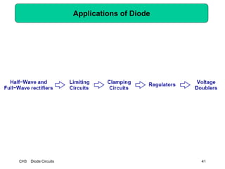
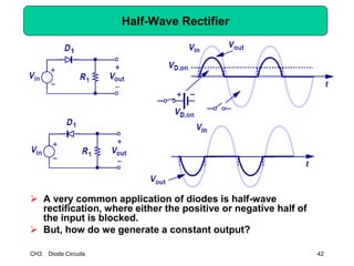
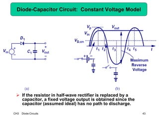
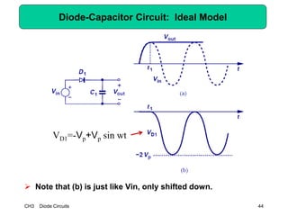
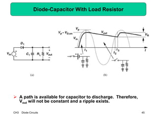
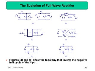
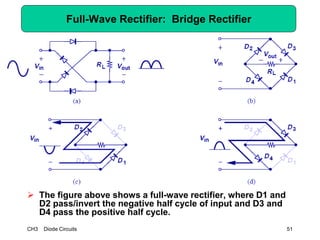
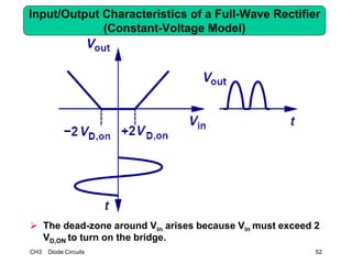
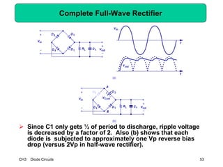

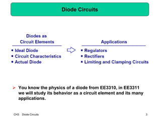
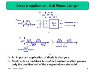
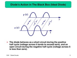
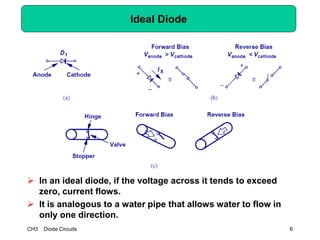
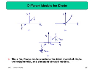
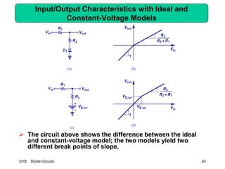
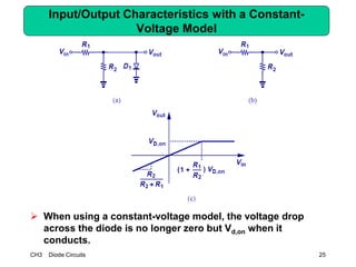
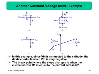
This document describes diode circuits and their applications. It begins with an overview of ideal, constant voltage, and exponential diode models. It then covers half-wave and full-wave rectification used in applications like phone chargers. The document also discusses limiter circuits, small signal analysis around operating points, and using incremental resistance to simplify nonlinear circuit analysis. Key applications of diodes in rectification, signal strength indicators, and logic gates are presented.