Download as PDF, PPTX

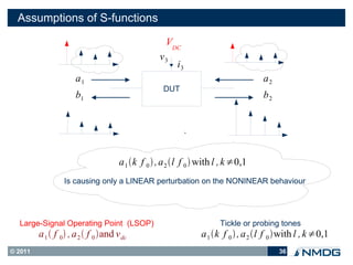
![S-parameter Design- and Test-Cycle for Linear Applications
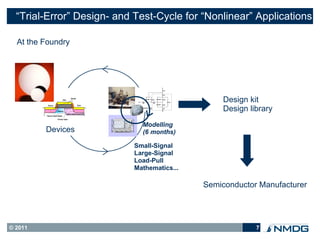
At the Foundry
Design kit
Design library
Passive [S-parameter based]
S-parameters
Devices
Semiconductor Manufacturer
© 2011 4](https://image.slidesharecdn.com/nm700sfunctionspdf3280-111117114841-phpapp02/85/S-functions-Presentation-The-S-parameters-for-nonlinear-components-Measure-Model-Verify-Simulate-4-320.jpg)
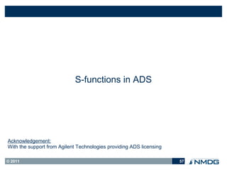
![S-parameter Design- and Test-Cycle for Linear Applications
At the Semiconductor Manufacturer
Design Chips S-parameters Design kit
Design library
[S-parameter based]
Iterations almost completely eliminated
Design Houses System Manufacturers
© 2011 5](https://image.slidesharecdn.com/nm700sfunctionspdf3280-111117114841-phpapp02/85/S-functions-Presentation-The-S-parameters-for-nonlinear-components-Measure-Model-Verify-Simulate-5-320.jpg)


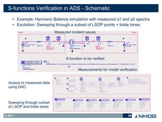
![The S-function Design- and Test-Cycle for Active Devices
At the Foundry
Design kit
Design library
[S-functions based (*)]
Devices S-Functions
Semiconductor Manufacturer
(*) S-functions for different applications
© 2011 10](https://image.slidesharecdn.com/nm700sfunctionspdf3280-111117114841-phpapp02/85/S-functions-Presentation-The-S-parameters-for-nonlinear-components-Measure-Model-Verify-Simulate-10-320.jpg)
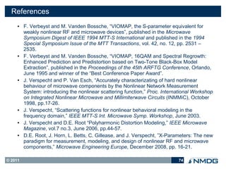
![The S-function Design- and Test-Cycle for Active Devices
At the Semiconductor Manufacturer
Improving S-functions with application-specific information
Design Chips S-functions Design kit
Design library
[S-functions based]
Reducing the number of iterations
Design Houses System Manufacturers
© 2011 11](https://image.slidesharecdn.com/nm700sfunctionspdf3280-111117114841-phpapp02/85/S-functions-Presentation-The-S-parameters-for-nonlinear-components-Measure-Model-Verify-Simulate-11-320.jpg)


![S-functions Verification in MWO - Frequency Domain
HBT UNER2
ID=X1
Mag1=0
Ang1=0 Deg
Mag2=0
Ang2=0 Deg
Mag3=0
Ang3=0 Deg
Fo=2 GHz
Zo=50 Ohm
PORT _PS1
P=1 1 2
Z=50 Ohm
PStart=-20 dBm BIAST EE 2
PStop=8 dBm ID=X2 PORT
PStep=1 dB 3:Bias P=2
SUBCK T
2 RF 1 1 Z=50 Ohm
RF & ID=S1
DC NET ="EPA_120_B "
DC
3 DCVS
ID=V1
V=DC2val V
DCVS
ID=V2
V=DC 1val V
Po with swept Pin Gain and Phase with swept Pin
40 20
19.5
20 19
F0 18.5
DB(|LSSnm(PORT_2,PORT_1,1,1)|)[1,X]
0 18 Swept Power.AP_HB
Ang(LSSnm(PORT_2,PORT_1,2,1))[1,X] (Deg)
17.5 Swept Power.AP_HB
-20 17
150
2F0
-40 100
DB(|Pcomp(PORT_2,1)|)[1,X] (dBm)
Swept Power.AP_HB
50
3F0 DB(|Pcomp(PORT_2,2)|)[1,X] (dBm)
-60 Swept Power.AP_HB
DB(|Pcomp(PORT_2,3)|)[1,X] (dBm)
Swept Power.AP_HB
0
-80 -50
-20 -15 -10 -5 0 5 10 -20 -15 -10 -5 0 5 10
Power (dBm) Power (dBm)
© 2011 68](https://image.slidesharecdn.com/nm700sfunctionspdf3280-111117114841-phpapp02/85/S-functions-Presentation-The-S-parameters-for-nonlinear-components-Measure-Model-Verify-Simulate-68-320.jpg)
![S-functions Verification in MWO - Time Domain
Vtime(V_METER.VM1,1)[*,T] (V) Itime(I_METER.AMP1,1)[*,T] (mA)
HBTUNER2 Waveform Tests.AP_HB Waveform Tests.AP_HB
ID=X1
Mag1=0
Ang1=0 Deg
Mag2=0
Ang2=0 Deg
Mag3=0
IV
Ang3=0 Deg 250
Fo=2 GHz
SUBCKT Zo=50 Ohm
PORT_PS1 ID=S1 200
P=1 NET="EPA_120_B" 1 2
Z=50 Ohm
PStart=-20 dBm BIASTEE 2 150
PStop=8 dBm ID=X2 PORT
PStep=1 dB I_METER 3:Bias P=2
2 RF 1 1 ID=AMP1 Z=50 Ohm 100
RF &
DC
DC 50
3 V _METER DCVS
ID =VM1 ID=V1
V=DC2val V
0
15
DCVS
ID=V2
V=DC1val V
10
5
DB(|Pcomp(PORT_2,1)|)[1,X] (dBm) DB(|Pcomp(PORT_2,2)| )[1,X] (dBm) DB(|Pcomp(PORT_2,3)|)[1,X] (dBm)
Waveform Tests.AP_HB Waveform Tests.AP_HB Waveform Tests.AP_HB0
0 0.2 0.4 0.6 0.8 1
Harmonics
40 Time (ns)
20
0
-20
-40
-60
-80
-20 -10 0 8
Power (dBm)
© 2011 69](https://image.slidesharecdn.com/nm700sfunctionspdf3280-111117114841-phpapp02/85/S-functions-Presentation-The-S-parameters-for-nonlinear-components-Measure-Model-Verify-Simulate-69-320.jpg)


The document discusses S-functions, which are proposed as behavioral models for nonlinear components and applications, analogous to how S-parameters are used for linear components and applications. S-functions aim to simplify design and testing of nonlinear RF/microwave circuits by providing a uniform characterization approach, as S-parameters do for linear circuits. By extracting S-functions from a component, its nonlinear behavior can be modeled and its performance can be simulated, enabling more efficient system-level design and easier comparison to measurements during manufacturing testing. The document outlines benefits of the S-function approach and similarities to the established S-parameter methodology.