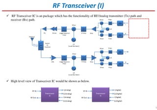
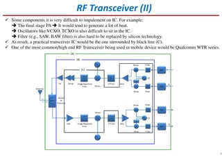
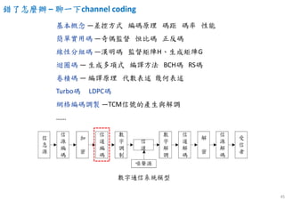
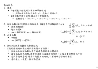
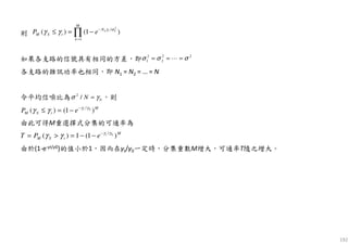
RF Transceiver (I)
RFTransceiver IC is an package which has the functionality of RF/Analog transmitter (Tx) path and
receiver (Rx) path.
High level view of Transceiver IC would be shown as below.
5
6.
Some components itis very difficult to impalement on IC. For example:
The final stage PA It would tend to generate a lot of heat.
Oscillators like VCXO, TCXO is also difficult to sit in the IC.
Filter (e.g., SAW, BAW filter) is also hard to be replaced by silicon technology.
As result, a practical transceiver IC would be the one surrounded by black line (C).
One of the most common/high end RF Transceiver being used in mobile device would be Qualcomm WTR series.
RF Transceiver (II)
6
7.
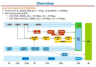
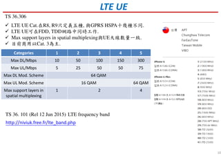
Overview
Long Term Evolution(LTE) Definition:
4G ITU的定義, 靜態DL傳輸速率 = 1Gbps, 高速移動DL = 100Mbps.
IMT-Advanced的4G標準
• LTE FDD: 20MHz, DL = 150 Mbps, UL = 40 Mbps.
• LTE TDD (TD-LTE): 20MHz, DL = 100 Mbps, UL = 50 Mbps.
7
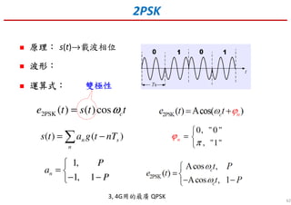
12
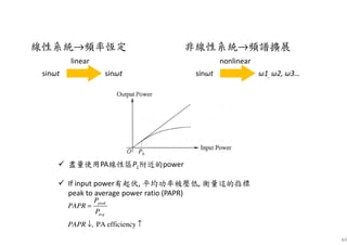
調製 = 頻譜搬移Why ?
Antenna gain is proportional to the electric size of the antenna. f↑, G↑
e.g., 麥克風f = 10 kHz, λ = 30 km, 30 km antenna…
f ↑ available bandwidth ↑
e.g., TV BW = 6 MHz
• 10% BW of VHF @60 MHz for 1channel
• 1% BW of U-band @60 GHz for 100 channels
管理
• Licensed spectrum
• Unlicensed spectrum
http://niviuk.free.fr/lte_band.php
https://www.slideshare.net/peichechang/lteu-note
13.
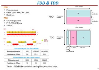
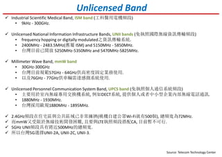
Unlicensed Band
Industrial ScientificMedical Band, ISM band (工科醫用電機頻段)
• 9kHz - 300GHz.
Unlicensed National Information Infrastructure Bands, UNII bands (免執照國際無線資訊傳輸頻段)
• frequency hopping or digitally modulated之資訊傳輸系統.
• 2400MHz - 2483.5MHz(舊屬 ISM) and 5150MHz - 5850MHz.
• 台灣目前已開放 5250MHz-5350MHz and 5470MHz-5825MHz.
Millimeter Wave Band, mmW band
• 30GHz-300GHz
• 台灣目前規範57GHz - 64GHz供高密度固定業務使用.
• 以及76GHz - 77GHz供車輛雷達感測系統使用.
Unlicensed Personnel Communication System Band, UPCS band (免執照個人通信系統頻段)
• 主要用於室內無線專用交換機系統, 例如DECT系統, 提供個人或者中小型企業內部無線電話通訊.
• 1880MHz - 1930MHz.
• 台灣採用歐規1880MHz - 1895MHz.
Source: Telecom Technology Center
2.4GHz頻段在住宅區與公共區域已非常擁擠(桃機自建公眾Wi-Fi就有500個), 總頻寬為72MHz.
而mmW又受限於無線技術開發困難, 且要與LTE執照頻段搭配CA, 目前暫不可行.
5GHz UNII頻段具有將近500MHz的總頻寬.
所以台灣5G選擇UNII-2A, UNII-2C, UNII-3.
15
BB signal
Carrier signal
RFsignal
BB signal spectrum
RF signal spectrum
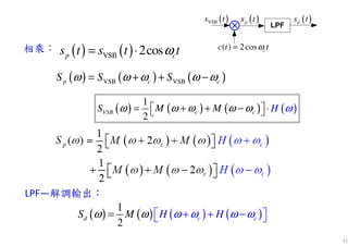
( ) coss t tω=
cos( ) cos( )
( ) ( )cos
2
c c
RF c
t t
s t s t t
ω ω ω ω
ω
− + +
= =
[ ]
2
( ) { ( )}
1
( ) { ( )cos } ( ) ( )
2
1 1
( )cos ( )cos ( ) ( ) ( )cos(2 )
2 2
RF c c c
RF c c c
S F s t
S F s t t S S
r t t s t t s t s t t
ω
ω ω ω ω ω ω
ω ω ω
=
= = − + +
= = +Demodulation →
LPF
Q: 同頻同相(相干解調) 難在…?
1 1
( )cos( ) ( )cos ( )cos(2 )
2 2
RF c cr t t s t s t tω φ φ ω φ+ = + +
相干解調相干解調相干解調相干解調
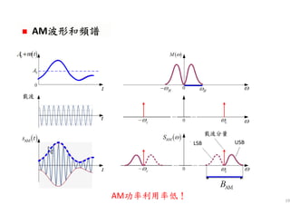
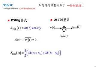
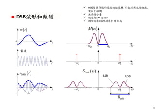
Modulation
24
1 1
cos sscoins in
2 2
m c cmm mt A tA t tωωω ω+=
( ) cosm mm t A tω=設
( ) cos cosDSB m m cs t A t tω ω= ⋅
( ) ( )LSB
1
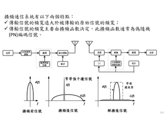
cos
2
m c ms t A tω ω−=
( ) ( )
1 1
cos sin
2 2
c ct tm tm t ω ω
∧
+=
( ) ( )
1
cos c
2
1
os
2
m c m m c mA tA tω ω ω ω= + +−
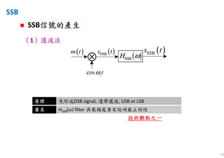
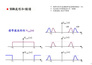
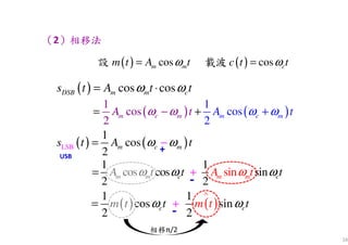
((((2))))相移法
( ) cos cc t tω=載波
USB
+
-
-
相移π/2
25.
25
1 0
where sgn
10
ω
ω
ω
>
=
− <
,
,
傳遞函數傳遞函數傳遞函數傳遞函數::::
( )
( ) sgn
( )
h
M
H j
M
ω
ω ω
ω
∧
= = −
( )
1
2
m t
( )SSBs t
⊗cos ctω
⊗
±
( )
1
2
m t
∧
( )
1
sin
2
cm t tω
∧
( )
1
cos
2
cm t tω
( )hH ω / 2π−
( )m t
∧
是m(t)的希爾伯特變換
Hilbert transform
含義含義含義含義::::幅度不變, 相移 π/2
技術難點之二技術難點之二技術難點之二技術難點之二
( ) ( ) ( )
1 1
cos sin
2 2
SSB c cs t m t t m t tω ω
∧
= ±
+LSB
-USB
物理意義: m(t)通過傳遞函數-jsgnω的濾波器即可得到 ˆ ( )m t
要求要求要求要求
Hh(ω)對m(t)的所有頻率分量
精確相移 π/2
解決: Weaver modulator
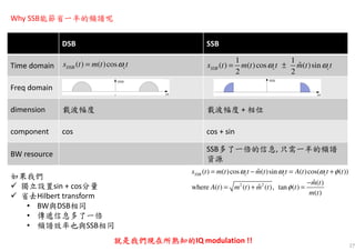
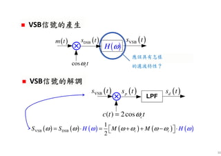
DSB SSB
Time domain
Freqdomain
dimension 載波幅度 載波幅度 + 相位
component cos cos + sin
BW resource
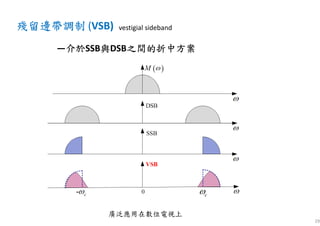
SSB多了一倍的信息, 只需一半的頻譜
資源
27
Why SSB能節省一半的頻譜呢
1 1
ˆ( ) ( )cos ( )sin
2 2
SSB c cs t m t t m t tω ω= ±( ) ( )cosDSB cs t m t tω=
2 2
ˆ( ) ( )cos ( )sin ( )cos( ( ))
ˆ ( )
ˆwhere ( ) ( ) ( ), tan ( )
( )
SSB c c cs t m t t m t t A t t t
m t
A t m t m t t
m t
ω ω ω φ
φ
= − = +
−
= + =
如果我們
獨立設置sin + cos分量
省去Hilbert transform
• BW與DSB相同
• 傳遞信息多了一倍
• 頻譜效率也與SSB相同
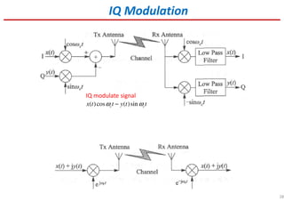
就是我們現在所熟知的就是我們現在所熟知的就是我們現在所熟知的就是我們現在所熟知的IQ modulation !!
34
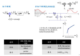
Kf =rad/(s•V)
Kp=rad/VPM:
FM::::
( )( )pKt m tϕ =
( )
( )f
d t
m t
dt
K
ϕ
=
( ) cos[ ( ])m cs t A t tϕω= +
FM是相位偏移隨m(t)的積分呈線性變化
如果預先不知道調製信號m(t)的具體形式, 則無法
判斷已調信號是調相信號還是調頻信號
PM是相位偏移隨調製信號m(t)線性變化
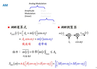
35.
35
單音調制單音調制單音調制單音調制FM與與與與PM
( ) cos[( )]
( ) cos[ cos ] cos[ cos ]
,
PM c p
PM c p
p
c
p
m
m
m p m
s t A t K m t
s t A t K A t A t m t
m K A
ω
ω ω ω ω
= +
= +
=
= +
用它對載波進行相位調製
調相指數 表示最大的相位偏移
( ) cos cos2
( ) cos[ ( ) ]
( ) cos[ cos ] cos[ sin ]
m m m m
FM c f
FM c f m m c f m
f m
f
m m m
f m
f m
m t A t A f t
s t A t K m d
s t A t K A d A t m t
K A f
m
f
K A
f m f
ω π
ω τ τ
ω ω τ τ ω ω
ω
ω ω
ω
= =
= +
= + = +
∆ ∆
= = =
∆ =
∆ = ⋅
∫
∫
用它對載波進行頻率調製
調頻指數,表示最大的相位偏移
最大角頻偏
最大頻偏
( ) cos cos2m m m mm t A t A f tω π= =
設調製信號為單一頻率的正弦波
t
( )m t
t
( )m t
t
( )tω
t
( )tω
cω
( )PMs t
t
( )FMs t
t
cω
37
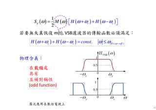
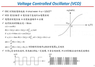
Voltage Controlled Oscillator(VCO)
OSC: LC諧振電路起振 → sinωt wave → ω = 1/(LC)0.5
VCO: 變容2極管 → 電容值可透過外加電壓控制
電壓控制電容值 → 改變振盪頻率→ 右圖
我們假設VCO輸出是一個cos
不管uc是啥形狀波形, 因為積分θ也一定連續, 不會出現跳變, 所以VCO輸出波形總是連續的
0 0
0
0 0
0
0
( ) cos ( )
( ) 2 ( ) 2 ( )
if ( ) 0 then ( ) cos(2 )
if ( ) then ( ) 2 2 ( )
( ) ( ) 2
( ) ( ) 2 ( )
t
c
c
t
c a
c
c t t
t f t t f t K u d
u t c t f t
u t v t f t K vd f t Kv t a
d
t t f Kv
dt
d
t t f Ku t
dt
θ
θ π φ π τ τ
π
θ π τ π
ω θ π
ω θ π
−∞
−
=
= + = +
= =
= = + = + +
= = +
= = +
∫
∫
VCO瞬時角頻率ω與控制電壓uc呈現性
38.
38
Phase Locked Loop(PLL)
相干相干相干相干解調最重要的元件之一解調最重要的元件之一解調最重要的元件之一解調最重要的元件之一
假設PLL input
output
{ }
( ) cos(2 )
( ) sin(2 )
1
( ) ( ) ( ) sin[2 ( ) ] sin[2 ( ) ]
2
LPF negative feedback " " VCO
1
( ) sin[2 ( ) ]
2
if then VCO tracking input signa
c
c
c c c c
c c c
c c
s t f t
c t f t
e t s t c t f f t f f t
u t f f t
f f
π φ
π φ
π φ φ π φ φ
π φ φ
= +
′ ′= +
′ ′ ′ ′= = − + − + + + +
→ → − →
−
′ ′= − + −
′ ≠
作為 控制電壓
l freq. until
1
if then ( ) sin[ ]
2
VCO ,
1
( ) [ ]
2
c c
c c c
c
f f
f f u t
u t
φ φ
φ φ φ φ
′ =
′ ′= = −
′ ′≈ − ⇒ ≈
控制靈敏度很高 只需很小的相差就可維持頻率鎖定
( )s t
( )c t
0
0
( ) 2 ( )
( ) ( ) 2 ( )c
t f t t
d
t t f Ku t
dt
θ π φ
ω θ π
= +
= = +
1. 表達式
2. 擾動行為
• (某種擾動原
因使φ’增大)
↑↓
↓↓↓
↓ ↓
39.
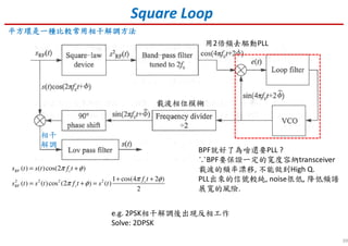
39
Square Loop
平方環是一種比較常用相干解調方法平方環是一種比較常用相干解調方法平方環是一種比較常用相干解調方法平方環是一種比較常用相干解調方法
2 22 2
( ) ( )cos(2 )
1 cos(4 2 )
( ) ( )cos (2 ) ( )
2
RF c
c
RF c
s t s t f t
f t
s t s t f t s t
π φ
π φ
π φ
= +
+ +
= + =
用2倍頻去驅動PLL
相干
解調
BPF就好了為啥還要PLL ?
∵BPF要保證一定的寬度容納transceiver
載波的頻率漂移, 不能做到High Q.
PLL出來的信號較純, noise很低, 降低頻譜
展寬的風險.
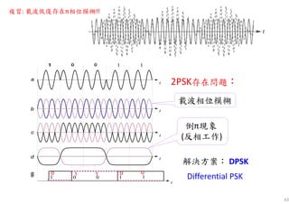
載波相位模糊
e.g. 2PSK相干解調後出現反相工作
Solve: 2DPSK
40.
40
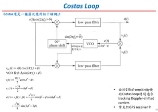
Costas Loop
Costas環環環環是是是是一種一種一種一種廣泛應用廣泛應用廣泛應用廣泛應用相干解調法相干解調法相干解調法相干解調法
• 由於2倍的sensitivity使
的Costasloop特別適合
tracking Doppler-shifted
carriers
• 常見於GPS receiver中
1
2
2
1 2
2
( ) ( )cos(2 )
VCO sin(2 )
( )
( ) cos( )
2
( )
( ) sin( )
2
( )
( ) ( ) ( ) sin( )cos( )
4
( )
sin(2 2 )
8
RF c
c
s t s t f t
f t
s t
v t
s t
v t
s t
e t v t v t
s t
π φ
π φ
φ φ
φ φ
φ φ φ φ
φ φ
= +
′+
′= −
′= −
′ ′= = − −
′= −
輸出為
sin 2( )φ φ′−VCO使相差
盡可能小
42
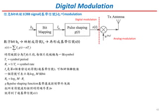
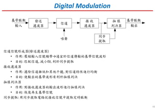
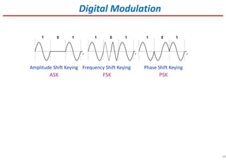
Digital Modulation
信息信息信息信息bit映射到映射到映射到映射到BB signal(基帶信號基帶信號基帶信號基帶信號)也叫也叫也叫也叫modulation
數字bitbk → 映射成符號In → 再形成基帶信號s(t)
2
2
( ) ( )
, symbol
symbol period
1/ symbol rate
( ),
log bit
log
pulse shaping function
( )
n s
n
s
s
s s
n
b s
s t I g t nT
T
T
R T
I n M
M
R M R
g
s t
= −
=
= =
= ⋅
∑
時間被劃分為 的片段 每個片段被稱為一個
是第 個要發送的符號 複基帶信號 可取 個離散值
一個符號可表示為 個
為 基帶濾波控制帶外洩漏
把所有符號波形按照時間順序累加
就得到了複基帶信號
Analog modulation
Digital modulation
( )y t
()C ω
{ }na
( )d t
48
Digital Modulation
( ) ( )
( ) ( ) ( ) ( )
1
( ) ( )
2
( ) ( ) ( ) ( )
1
( ) ( )
2
n s
n
T n T s
n
j t
T T
T R
j t
d t a t nT
s t d t g t a g t nT
g t G e d
H G C G
h t H e d
ω
ω
δ
ω ω
π
ω ω ω ω
ω ω
π
∞
=−∞
∞
=−∞
∞
−∞
∞
−∞
= −
= ∗ = −
=
=
=
∑
∑
∫
∫
s(t)
[ ]0 0 0 0
( ) ( ) ( ) ( ) ( ) ( )
( ) ( ) ( ) ( )
R n S R
n
s k n s R s
n k
r t d t h t n t a h t nT n t
r kT t a h t a h k n T t n kT t
∞
=−∞
≠
= ∗ + = − +
+ = + − + + +
∑
∑
r(t) 0( )sr kT t+⊕
{ }na′0,1,0,1 or -1,1,-1,1
對應的BB signal
gT(t): impulse response
分析前先把model建好
nR(t)是加性雜訊n(t)經過接
收濾波器後輸出的雜訊
為了確定第k個碼元 ak 的取值, 首先應
在t = kTs + t0 時刻上對r(t)進行抽樣, 以確
定r(t)在該樣點上的值
50
( )h t
0t0sT t+
( )h t
0t 02 sT t+0sT t+
[ ]0(ISI )n s
n k
a h k n T t
≠
= − +∑
( ) 0+ =0n s
n k
a h k n T t
≠
− ∑
若能使若能使若能使若能使:
, 則無則無則無則無ISI
怎麼做怎麼做怎麼做怎麼做????
做不到做不到做不到做不到 關注抽樣時刻關注抽樣時刻關注抽樣時刻關注抽樣時刻
等等等等Ts的零的零的零的零點點點點
由於an是隨機的,要想通過各項相互抵消使碼間串擾為0是不行的
這就需要對h(t)的波形提出要求。
若讓h [(k-n)Ts +t0] 在Ts+ t0 、2Ts +t0等後面碼元抽樣判決時刻上正好為0,就能消除碼間串擾
這就是消除碼間串擾的基本思想
51.
51
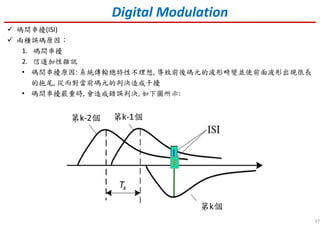
無碼間串擾無碼間串擾無碼間串擾無碼間串擾(ISI)的時域條件的時域條件的時域條件的時域條件
Digital Modulation
1, 0
()
0,
s
k
h kT
k
=
=
為其他整數 ( )
( )
( )
(2 1) /
(2 1) /
/
2
/
/
/
1
( ) ( )
2
1
( )
2
1
( )
2
2
1 2
( )
2
1 2
( )
2
( )
S
S
S
S
S
S
S
S
S
S
j t
j kT
S
i T
j kT
S i T
i
s
T
j kT j ik
S T
i S
T
j kT
T
i S
h t H e d
h kT H e d
h kT H e d
i
T
i
h kT H e e d
T
i
H e d
T
F f
ω
ω
π ω
π
π ω π
π
π ω
π
ω ω
π
ω ω
π
ω ω
π
π
ω ω
π
ω ω
π
π
ω ω
π
ω
∞
−∞
∞
−∞
+
−
′
−
′
−
=
=
=
′ = −
′ ′= +
′ ′= +
=
∫
∫
∑∫
∑∫
∑∫
/
/
( )
2
S
S
S
S
jn T
n
n
T
jn TS
n T
e
T
f F e d
ω
π ω
π
ω ω
π
−
−
=
∑
∫
無碼間串擾無碼間串擾無碼間串擾無碼間串擾(ISI)的的的的頻頻頻頻域條件域條件域條件域條件
2
( ) ,S
i S S
i
H T
T T
π π
ω ω+ = ≤∑
抽樣脈衝
分段分段分段分段
積分積分積分積分
求和求和求和求和
52.
52
2
( ) ,S
iS S
i
H T
T T
π π
ω ω+ = ≤∑
Ts Ts
2
Ts
3
i=1(d)
Ts
H( )
Ts
3
- Ts
2
-
Ts
-
Ts Ts
2
Ts
3
(a)
檢驗或設計H(ω)能否消除ISI的理論依據
物理物理物理物理含義含義含義含義:
切割切割切割切割, 平移平移平移平移, 對折對折對折對折, 疊加成理想疊加成理想疊加成理想疊加成理想LPF
以以以以Rs = 1/Ts的速率傳輸的速率傳輸的速率傳輸的速率傳輸
則無則無則無則無ISI !!
53.
53
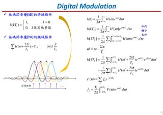
Digital Modulation
( )Hω
ST
π
−
ST
π0 ω
,
( )
0,
S
S
S
T
T
H
T
π
ω
ω
π
ω
≤
=
>
sin
( ) sinc( / )S
S
S
t
T
h t t T
t
T
π
π
π
= =
FT
若輸入資料以RB = 1/Ts波特的速率進行傳輸,則在抽樣時刻上不存在碼間串擾。
• 若以高於1/Ts波特的碼元速率傳送時,將存在碼間串擾。
• 通常將此頻寬B = 1/(2Ts)稱為Nyquist頻寬頻寬頻寬頻寬fN,將RB稱為Nyquist速率速率速率速率。
此基帶系統所能提供的最高頻帶利用率η為 RB/B = 2, 這種特性陡峭在物理上是無法實現的
• 並且h(t)的振盪衰減慢, 使之對定時精度要求很高, 故不能實用。
How to solve ? 在fN奇對稱波形進行”圓滑”+”滾降”
Nyquist最窄頻寬 無ISI最高Baud Nyquist rate
無ISI BB最高頻帶利用率
54.
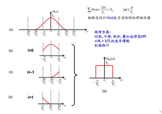
54
Digital Modulation
raised-cosine filterminimize ISI
(1 )
, 0
(1 ) (1 )
( ) [1 sin ( )],
2 2
(1 )
0,
S
S
S S
S S S
S
T
T
T T
H
T T T
T
α π
ω
π α π α π
ω ω ω
α
α π
ω
−
≤ <
− +
= + − ≤ <
+
≥
( ) 2 2 2
sin / cos /
/ 1 4 /
S S
S S
t T t T
h t
t T t T
π απ
π α
= ⋅
−
FT
/ Nf fα ∆≡
引入滾降係數
描述滾降程度
( )0 ~1
1
2
N
B N
B
f
f
R f
T
α ∆
=
= =
(1 )N NB f f fα∆= + = +
55.
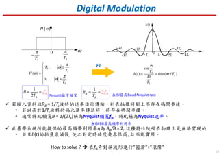
55
(1 )
, 0
(1) (1 )
( ) [1 sin ( )],
2 2
(1 )
0,
S
S
S S
S S S
S
T
T
T T
H
T T T
T
α π
ω
π α π α π
ω ω ω
α
α π
ω
−
≤ <
− +
= + − ≤ <
+
≥
( ) 2 2 2
sin / cos /
/ 1 4 /
S S
S S
t T t T
h t
t T t T
π απ
π α
= ⋅
−
FT
/ Nf fα ∆≡
Digital Modulation
root-raised-cosine (RRC) filter
實際應用中1個在Tx, 1個在Rx, raised-cosine RRC RRC= ⋅
√ ̄
√ ̄ ̄ ̄ ̄ ̄ ̄
余弦滾降濾波器特點
1. 特性易實現
2. Response曲線拖尾收斂快, 擺幅較小
BUT代價
1. BW↑
2. 頻帶利用率η↓
57
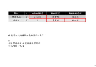
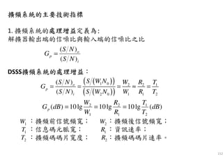
部分響應技術部分響應技術部分響應技術部分響應技術 → 提高頻譜利用率提高頻譜利用率提高頻譜利用率提高頻譜利用率單個sinx/x波形: 拖尾收斂慢
2個相距Ts sinx/x波形相加: 拖尾衰減快
( ) 2 2
sin ( ) sin ( )
2 2 cos /4
1 4 /( ) ( )
2 2
S S
S S S
S S S
S S
T T
t t
T T t T
T T t Tt t
T
g t
T
π π
π
π π π
+ −
= + =
− + −
sin ( )
2
( )
2
B
B
B
B
T
t
T
T
t
T
π
π
+
+
sin ( )
2
( )
2
B
B
B
B
T
t
T
T
t
T
π
π
−
−
( )
2 cos ,
2
0,
S
S
S
S
T
T
T
G
T
ω π
ω
ω
π
ω
≤
=
>
FT
1
2
1 1
/ / 2 ( /
Ny
)
2
quist
S
B
S S
B
T
R B B Hz
T T
η
=
= = =
頻寬
• 若g(t)為傳送信號的波形且發送碼元的間隔為Ts
• 則本碼元的抽樣值僅受前一碼元相同幅值的串擾
58.
58
時域均衡時域均衡時域均衡時域均衡 → ISI↓
()H ω′
有有有有 ISI
ݔݔݔݔ()ݐ
( )H ω ( )T ω
無無無無 ISI
ݕݕݕݕ()ݐ有有有有誤差誤差誤差誤差
( ) ( ) ( ) ( )if equalizer
ISI
then ( ) ISIy t
HT THω ωωω =′∋插入
滿足無 的頻域條件
在抽樣時刻上無
( )
1
,
2 2
) ) ,
2 /
,
( ) ( )
(
( )
( )
( ) (
2
( )
( ) [ ] ( )
22
2
(
(
)
)
B
B
i B
B
i B B B
B
B
B
i B
jnT
n T n B
n n
jnB B
n
i B
B
T
T
i i
T
T T T
T
T
i TH
T
C e
i
T
T
T
T
h t F C t nT
T T
C e
i
H
T
H
H
H
T
T
H
T ω
ω
ω
ω
π
ω
π π π
ω
ω
ω
π
ω
π
π
ω
π
ω
δ
ω
ω
ω
π
ω
π
ω
ω
∞ ∞
− −
=−∞ =−∞
+
′ = ≤
+ ⋅ + = ≤
= ≤
+
= ⇔ = = −
=
+
=′
∑
∑
∑
∑ ∑
∑
帶入
是 為週期的函數
BB
B
TT
T
d
π
π ω−∫
由hT(t)構造出equalizer的結構: 橫向濾波器
( ) ( )T n B
n
h t C t nTδ= −∑
59.
59
Digital Modulation
t tt
Amplitude Shift Keying Frequency Shift Keying Phase Shift Keying
ASK PSKFSK
65
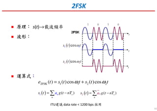
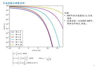
多進制數位調製原理多進制數位調製原理多進制數位調製原理多進制數位調製原理
2進制: 每個 symbol只攜帶 1 bit 信息
M log2M bit
Rb = bit rate = bps = [bit/sec]
RB = symbol rate
= #symbol/sec = [Baud]
B
b
b
R Baud
B Hz
R bit
B s Hz
η
η
=
= ⋅
2logb BR R M=
Rb 固定, 增加進制數M↑, 可降低RB↓
減少信號BW, 節省頻率資源
RB 固定, 增加進制數M↑, 可增大Rb↑
在相同BW內傳輸更多bit, ηb↑
目的: 就是為了提高信道的頻帶利用率!!
代價:
• BER↑(判決範圍減小), 系統複雜
• 若要保證一定的BER, SNR↑, 發射功率增大, 耗能…
69
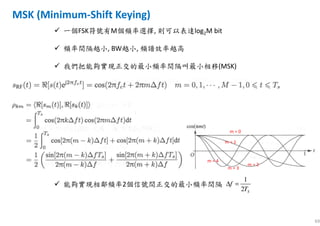
一個FSK符號有M個頻率選擇, 則可以表達log2M bit
頻率間隔越小,BW越小, 頻譜效率越高
我們把能夠實現正交的最小頻率間隔叫最小相移(MSK)
1
2 S
f
T
∆ =能夠實現相鄰頻率2個信號間正交的最小頻率間隔
m = 0
m = 3
m = 2
m = 1
m = 4
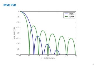
MSK (Minimum-Shift Keying)
76
多進制數位調製原理多進制數位調製原理多進制數位調製原理多進制數位調製原理
2進制: 每個 symbol只攜帶 1 bit 信息
M log2M bit
Rb = bit rate = bps = [bit/sec]
RB = symbol rate
= #symbol/sec = [Baud]
B
b
b
R Baud
B Hz
R bit
B s Hz
η
η
=
= ⋅
2logb BR R M=
Rb 固定, 增加進制數M↑, 可降低RB↓
減少信號BW, 節省頻率資源
RB 固定, 增加進制數M↑, 可增大Rb↑
在相同BW內傳輸更多bit, ηb↑
目的: 就是為了提高信道的頻帶利用率!!
代價:
• BER↑(判決範圍減小), 系統複雜
• 若要保證一定的BER, SNR↑, 發射功率增大, 耗能…
77.
77
( )
2
2
1
, BPSK
2
1
11 , QPSK ,where
2 2 log
sin , MPSK for 4
e
e b
e
P erfc r
r r
P erfc r
M
P erfc r M
M
π
=
= − − =
≈ ≥
代價:
• BER↑(判決範圍減小), 系統
複雜
• 若要保證一定的BER, SNR↑,
發射功率增大, 耗能…
多進制數位調製原理多進制數位調製原理多進制數位調製原理多進制數位調製原理
85
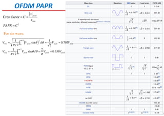
OFDM PAPR
2
Crest factorpeak
rms
x
C
x
PAPR C
= =
=
( )
/2 2
0
/2
0
1 1
sin 0.707
/ 2 2
1 2
sin 0.636
/ 2
rms peak peak peak
avg peak peak peak
V V d V V
V V d V V
π
π
θ θ
π
θ θ
π π
= = =
= = =
∫
∫
For sin wave:
ET
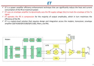
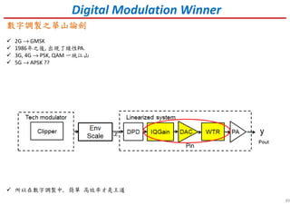
ET is apower amplifier efficiency enhancement technique that can significantly reduce the heat and current
consumption of the PA at maximum power.
ET uses an envelope amplifier to dynamically vary the PA supply voltage (Vcc) to track the envelope of the Tx
signal.
ET operates the PA in compression for the majority of output amplitudes, which in turn maximizes the
efficiency of the PA.
ET is a system-level solution that requires design and integration across the modem, transceiver, envelope
amplifier (QET4100/QFE3100/QFE1100), filters, and PAs.
87
88.
88
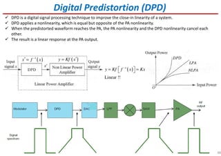
DPD is adigital signal processing technique to improve the close-in linearity of a system.
DPD applies a nonlinearity, which is equal but opposite of the PA nonlinearity.
When the predistorted waveform reaches the PA, the PA nonlinearity and the DPD nonlinearity cancel each
other.
The result is a linear response at the PA output.
Digital Predistortion (DPD)
( )y Kf x′=( )1
x f x−
′ =
( )1
Linear !!
y Kf f x Kx−
= =
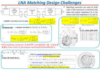
LNA Matching DesignChallenges
Matching networks are used on both
sides of the transistor to transform the
input and output impedance Z0 to the
source and load impedances ZS and ZL.
1.
GS GL const. gain circle
2.
Const. NF circle for GS
3.
LNA matching conclusion: ZS按照NF circle調到最小圈, 不過也要
兼顧GS Gain circle; ZL就conjugate matching用把Gain調到最大.
97
98.
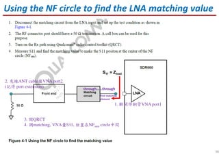
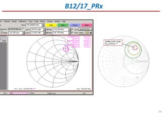
Using the NFcircle to find the LNA matching value
1. 斷開焊銅管VNA port1
2. 灰線ANT cable接VNA port2
(記得 port extension)
3. 開QRCT
4. 調matching, VNA量S11, 位置在NFmin circle中間
through……through
First matching
element
98
99.
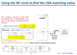
LNA matching conclusion:ZS 按 照 NF
circle調到最小圈, 不過也要兼顧GS Gain
circle; ZL就conjugate matching用把Gain
調到最大.
in
Using the NF circle to find the LNA matching value
Γ௦
Γ
為了首要兼顧NF circle
不然Γ௦, Γ通常幾乎都為complex conjugate.
ࢣ = ࡿ in next page 99
109
Optimum Receiver forAWGN Channels
Maximize a posteriori probability (MAP)
|
ˆ arg max ( | )
( | ) ( )
( | )
( )
p
p p
p
p
=
=
Ψ r
Ψ
Ψ Ψ r
r Ψ Ψ
Ψ r
r
The ML estimate of ψ is the value that maximizes p(r| ψ).
The MAP estimate is the value of ψ that maximizes the a posteriori probability density function
Maximum-likelihood (ML)
= Least-squares (only in Gaussian distribution)
| 1 2 3
|
( ) ( ) ( )
{ ( )}
ˆ arg max ( , , | )
ˆ arg max ( | )
r s
s
r t s t n t
H
s p r r r s
p
= +
= +
=
= r Ψ
Ψ
r s Ψ n
Ψ r Ψ
111
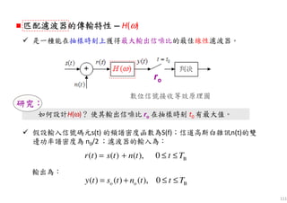
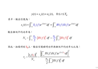
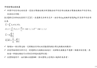
如何設計H(ω)? 使其輸出信噪比 ro在抽樣時刻 t0 有最大值。
研究研究研究研究::::
匹配濾波器匹配濾波器匹配濾波器匹配濾波器的的的的傳輸特性傳輸特性傳輸特性傳輸特性 — H(ω)
是一種能在抽樣時刻上獲得最大輸出信噪比的最佳線性濾波器。
ro
數位信號接收等效原理圖
輸出為:
假設輸入信號碼元s(t) 的頻譜密度函數為S(f);信道高斯白雜訊n(t)的雙
邊功率譜密度為 n0/2 ;濾波器的輸入為:
B( ) ( ) ( ), 0r t s t n t t T= + ≤ ≤
o o B( ) ( ) ( ), 0y t s t n t t T= + ≤ ≤
112.
112
2 2
( ))( ) )( (j f t j
o
f t
os t e dS f H f Sf e df fπ π
∞ ∞
−∞ −∞
= =∫ ∫
其中,輸出信號為:
輸出雜訊平均功率為:
因此,抽樣時刻 t0上,輸出信號瞬時功率與雜訊平均功率之比為:
( ) ( ) ( ), 0o o By t s t n t t T= + ≤ ≤
113.
113
0
2 22
o
0 2
() )
2
(
(
)
j f t
df df
r
n
df
eH f
H f
S f π∞ ∞
−∞ −∞
∞
−∞
⋅
≤
∫ ∫
∫
2
2 2
( ) ( )( ) ( )X f X fdf df dY f fY f
∞ ∞ ∞
−∞ −∞ −∞
⋅≤∫ ∫ ∫
2
2 2
( ) ( )( ) ( )X f X fdf df dY f fY f
∞ ∞ ∞
−∞ −∞ −∞
⋅≤∫ ∫ ∫
( )X f ( )Y f
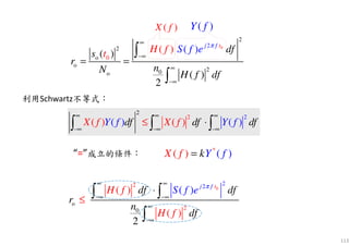
利用Schwartz不等式:
“=”成立的條件:
0
2
2
o
o
20o
2
0( )
( )
2
( ) ( ) j tf
S f dfs
r
nN H f d
H ft e
f
π∞
−∞
∞
−∞
= =
∫
∫
*
( )) (kYX f f=
114.
114
max
0
2
o
E
r
n
=
0* 2
(( )) j f t
S ff eH k π−
=僅當僅當僅當僅當
2
o
0 / 2
( ) dfS
n
f
r
∞
−∞∫≤≤≤≤
式中,
2 2
( ( )S f df s t dt E
∞ ∞
−∞ −∞
= =∫ ∫)
o
0
2E
r
n
即 ≤≤≤≤
)( ()X f H f=
02
( )( ) j f t
Y f S f e π
=
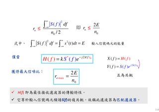
獲得最大獲得最大獲得最大獲得最大信噪比信噪比信噪比信噪比::::
H(f) 即為最佳接收濾波器的傳輸特性。
它等於輸入信號碼元頻譜S(f)的複共軛。故稱此濾波器為匹配濾波器匹配濾波器匹配濾波器匹配濾波器。
H(f) 即為最佳接收濾波器的傳輸特性。
它等於輸入信號碼元頻譜S(f)的複共軛。故稱此濾波器為匹配濾波器匹配濾波器匹配濾波器匹配濾波器。
互為共軛
輸入信號碼元的能量
115.
115
0* 22 2
()(( )) j fj f j ttt f
H f e df k eft eh dfS ππ π
∞ ∞
−
−∞ −∞
= =∫ ∫
0( )
*
22
( ) j t tf j f
k e dfs e dπ τ π
τ τ
∞
− −
−∞
∞
−
−∞
=
∫ ∫
00 (( )) ( )k s dt t s tk tττ τδ
∞
−∞
= =− −+∫
02 ( )
( )j f t t
k e df s dπ τ
τ τ
∞ ∞
− +
−∞ −∞
= ∫ ∫
0 22 ( - )
( )1 j f t j ft
k e dfe s dτπ π
τ τ
∞ ∞
−
−
∞ −∞
⋅
= ∫ ∫
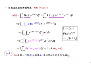
匹配濾波器匹配濾波器匹配濾波器匹配濾波器的的的的衝激衝激衝激衝激響響響響應應應應— h(t) ( )H f⇔
含義含義含義含義::::
h(t)是輸入信號s(t)的鏡像s(-t)及時間軸上的平移(右移t0).
116.
116
0
( )s t
tTB-TB
()h t
0 tt0t0 -TB
因此, t0 ≥ TB
通常取 t0 = TB
0 0( ) ( ) [ ( )]h t s t t s t t= − = − −
問題: t0 = ????
鏡像鏡像鏡像鏡像及右移右移右移右移
圖解::::
這時 h(t) = s(TB-t)
117.
117
o ( )( ) ( ) ( ) ( )s t s t h t s ht dττ τ
∞
−∞
= ∗ = −∫
0) )( (ks ts t dτ ττ
∞
−∞
−= −∫
0 0( ) ( ) ( )k s x s x t t dx kR t t
∞
−∞
= + − = −∫
k=1 時
0( ) ( )os t R t t= −
t =t0 時
2
-0max[ ( )] ( ) ( ) ( )0o os t s R s Et tt d
∞
∞
= = = =∫
匹配濾波器匹配濾波器匹配濾波器匹配濾波器的的的的輸出信號輸出信號輸出信號輸出信號— so(t)
匹配匹配匹配匹配濾波器濾波器濾波器濾波器可看成是一個計算輸入信號自相關函數的相關器可看成是一個計算輸入信號自相關函數的相關器可看成是一個計算輸入信號自相關函數的相關器可看成是一個計算輸入信號自相關函數的相關器!!
118.
118
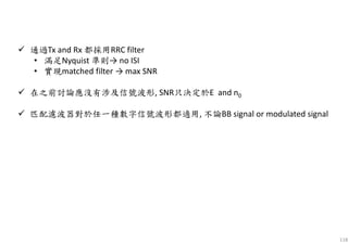
通過Tx and Rx都採用RRC filter
• 滿足Nyquist 準則→ no ISI
• 實現matched filter → max SNR
在之前討論應沒有涉及信號波形, SNR只決定於E and n0
匹配濾波器對於任一種數字信號波形都適用, 不論BB signal or modulated signal
121
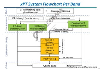
Channels
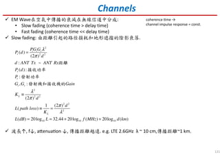
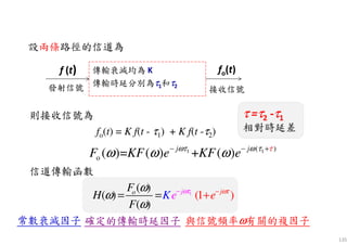
EM Wave在空氣中傳播的衰減在無線信道中分成:
• Slowfading (coherence time > delay time)
• Fast fading (coherence time << delay time)
Slow fading: 由距離引起的路徑損耗和地形遮擋的陰影衰落.
coherence Ɵme →
channel impulse response = const.
2
2 2
2
2 2
2 2
2
10 10 10
( )
(2 )
: ~
( ):
:
, :
(2 )
1 (2 )
( )
( ) 20log 32.44 20log ( ) 20log ( )
t t r
r
r
t
t r
L
L
PG G
P d
d
d ANT Tx ANT Rx
P d
P
G G Gain
K
d
d
L path loss
K
L dB L f MHz d km
λ
π
λ
π
π
λ
=
≡
≡ =
= = + +
距離
接收功率
發射功率
發射機和接收機的
波長↑, f↓, aƩenuaƟon ↓, 傳播距離越遠. e.g. LTE 2.6GHz λ ~ 10 cm,傳播距離~1 km.
122.
122
Channels
EM Wave在空氣中傳播的衰減在無線信道中分成:
• Slowfading (coherence time > delay time)
• Fast fading (coherence time << delay time)
Fast fading:
• Doppler effect
multipath多徑效應多徑效應多徑效應多徑效應
• 同相
• 反相: 移動λ /4, 相位+ - π/2
• 3G: 2GHz, λ~15 cm, λ /4 ~ 4 cm
• 人步速 = 1 m/s, 信道變化頻率 = 25次
• 10m/s, 信道變化頻率 = 250次
• 變化速度相對於陰影衰落是很快的 叫快衰落
(1 )
( ) cos[(1 )2 ] cos[(1 )2 ]
2cos(2 )cos(2 )
r s
s s
s s
v
f f
c
v v
r t f t f t
c c
v
f t f t
c
π π
π π
= +
= + + −
=
Doppler shift
1
coherent
Doppler
T
f
∝
∆
時間選擇性衰落(快衰落)
coherent Ɵme → 信號保持不變的時間
123.
123
0( ) ()
( ) ( ) ( )
( ) ( )
[ ] ( )
( )
( )
o
o
i i
i
f c t
r t s t
s t s t s t
t
S SC
n
ω ωω
= +
= = ∗
=
( )H Kω = dtωωϕ =)( dt
d
d
==
ω
ωϕ
ωτ
)(
)(⇒⇒⇒⇒
無失真傳輸理想信道無失真傳輸理想信道無失真傳輸理想信道無失真傳輸理想信道
幅頻特性 相頻特性 Group delay特性
o ( ) ( )ds t K s t t= −
( ) dj t
H eK ω
ω −
= ( ) ( )dh t K t tδ= −
固定的遲延
固定的衰減
這種情況稱為無失真傳輸這種情況稱為無失真傳輸
若輸入信號為s(t),則理想恒參信道的輸出:
input output
131
( )
( )
d
d
t
t
φω ω
τ ω
≠
≠
失真影響失真影響失真影響失真影響
( )H Kω ≠幅頻失真:
相頻失真:
: SNR
: ISI BER
→ ↓
→ ↑
對模擬信號 波形失真
影響
對數字信號 產生
: voice , vedio
: ISI BER
→ ↑
對模擬信號 影響不大 影響大
影響
對數字信號 產生
132.
132
( ) cosctAs t ω=
[ ] [ ]
[ ]
[ ]
[ ]
1 1 2 2
1
1
( ) ( )cos ( ) ( )cos ( )
( ) ( )
( ) ( )
( )cos ( )
cos
cos
c c
n c n
n
c
i
n
c
i
i i
i i
r t a t t t a t t t
a t t t
t
t
a t t
a t t
ω τ ω τ
ω τ
ω τ
ϕω
=
=
= − + −
+ −
= −
= +
∑
∑
⋯
multipath多多多多徑效應徑效應徑效應徑效應
經過n條路徑條路徑條路徑條路徑傳播(各路徑有時變時變時變時變的衰落衰落衰落衰落和時延時延時延時延))))
— 多徑傳播的影響
)()( tt ici τωϕ −= )()( tt ici τωϕ −=
傳輸時延
則接收信號接收信號接收信號接收信號為
設發送發送發送發送信號為
幅度恒定
頻率單一
第i條路徑
接收信號振幅
(時變時變時變時變的衰落衰落衰落衰落)
133.
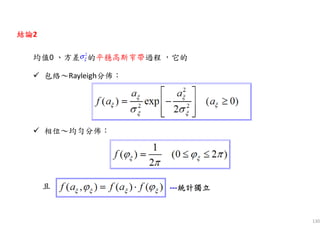
133
根據概率論中心極限定理:當 n
足夠大時,x(t)和y(t) 趨於正態分佈。
∑=
=
n
i
iitatX
1
cos)()( ϕ
∑=
=
n
i
ii tatY
1
sin)()( ϕ
同相 ~ 正交形式
包絡 ~ 相位形式
瑞利瑞利瑞利瑞利
分佈分佈分佈分佈
均勻均勻均勻均勻
分佈分佈分佈分佈
[ ]cos( ) ( )cV t t tω ϕ= +
1 1
( ) ( )cos cos ( )sin sin
( )cos ( )sin
n n
i i c i i c
i i
c c
r t a t t a t t
X t t Y t t
ϕ ω ϕ ω
ω ω
= =
= −
= −
∑ ∑
包絡相位
隨機緩變的
窄帶信號
134.
134
f∆
fcf
f
cf0
波形
發送信號發送信號 接收信號接收信號
頻譜
[ ]() co (s( ) )cr t V t t tω ϕ= +( ) cos ctAs t ω=
緩慢變化的包絡
結論結論結論結論
Multipath傳播使信號產生Rayleigh fading
Multipath傳播引起frequency spread
Multipath傳播引起數字信號ISI
135.
135
發射信號 接收信號
設兩條路徑的信道為
f (t)
fo(t)= K f(t - τ1) + K f(t -τ2)
信道傳輸函數
fo(t)
ττττ =ττττ2 -ττττ1
相對時延差
1
(1)
(
)
( )
(
)
o jj
KH
F
e e
F ωωτ τω
ω
ω
−−
+= =
則接收信號為
1 1( )
o ( )= ( ) + ( )j j
F KF e KF eωτ ω τ τ
ω ω ω− − +
常數衰減因子 確定的傳輸時延因子 與信號頻率ωωωω有關的複因子
傳輸衰減均為 K
傳輸時延分別為ττττ1和ττττ2
136.
136
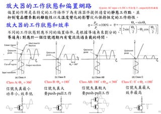
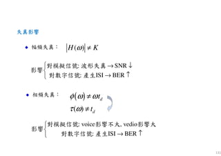
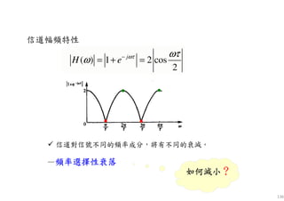
( ) 12 cos
2
j
H e ωτ ωτ
ω −
= + =
—頻率選擇性衰落頻率選擇性衰落頻率選擇性衰落頻率選擇性衰落
如何減小如何減小如何減小如何減小????
信道幅頻特性
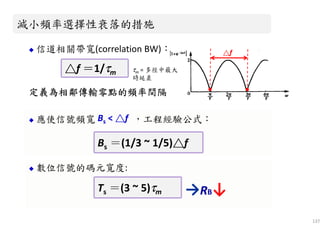
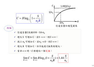
信道對信號不同的頻率成分,將有不同的衰減。
139
信道容量
指信道能夠無差錯傳輸時的最大平均資訊速率
S - 信號平均功率(W);B- 頻寬(Hz)
n0 -雜訊單邊(SSB)功率譜密度;N = n0B -雜訊功率(W)
連續信道連續信道連續信道連續信道容量容量容量容量
由Shannon資訊理論資訊理論資訊理論資訊理論可證,AWGN背景下的連續信道容量為:
——Shannon公式公式公式公式
等價等價等價等價::::
2016/04/30 Google Doodle Claude Shannon 100 歲冥誕
意義:若Rb ≤ C則總能找到一種信道編碼方式, 實現無差錯傳輸
140.
140
信道容量C依賴於B、S和n0
增大 S 可增加C,若S → ∞,則C→ ∞;
減小 n0 可增加 C,若n0 → 0,則C→ ∞;
增大 B 可增加 C,但不能使 C無限制增大。
當 B→ ∞ 時,C 將趨向一個定值:
結論:
2
0 0
lim lim log (1 ) 1.44
B B
S S
C B
n B n→∞ →∞
= + ≈
信道容量和頻寬關係
S/n0
S/n0
B
C 1.44(S/n0)
145
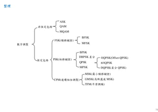
基本概念
1. 運算
• 2進制數字信號用01表示→單極性碼
•模2加→
• 2進制數字信→號用-11表示→雙極性碼
• 邏輯乘→
2. 相關函數: 任2信號間的相似程度. 設2個長度為N的序列a, b
• 非週期相關C
• 週期相關R
• a ≠ b 稱互相關, a = b 稱自相關
3. 正交函數
• 0相關
• a = {0000}, b = {0101}
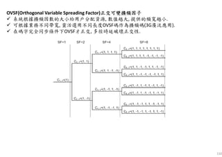
4. CDMA系統中的擴頻碼和位址碼
• 理想的擴頻碼和地址碼必須具備以下特性:
• 尖銳的自相關函數和幾乎處處為零的互相關函數
• 盡可能長的碼週期, 使干擾者難以通過擴頻碼的一小段去重建整個碼序列
• 足夠多的碼序列, 用來作為獨立的地址, 以實現碼分多址的要求
• 易於產生、複製、控制和實現
0 0 0, 0 1 1, 1 0 1, 1 1 0⊕ = ⊕ = ⊕ = ⊕ =
1 1 1, 1 1 1, 1 1 1, 1 1 1+ ×+ = + + ×− = − − ×+ = − − ×− = +
( )
1
0
1
,
0
1
0 1
1
1 0
0
N
i i
i
N
a b i i
i
a b N
N
C a b N
N
N
τ
τ
τ
τ
τ
τ τ
τ
− −
+
=
− +
−
=
≤ ≤ −
= − ≤ ≤
≥
∑
∑
( )
1
,
0
1 N
a b i i
i
R a b Z
N
ττ τ
−
+
=
= ∈∑
158
user
data
clock
carrier
phase
mod
PA RFFE
coherent
de-mod
phase
mod
clockLO
IF
filter
de-
mod
output
data
(1) userdata m(t)
(2) PN code p(t)
(3) c(t) = m(t) ⊕p(t)
(4) carrier
(5) modulated BPSK s1(t)
(6) s1(t) phase
(7) s2(t) phase 跟著PN走
(8) IF phase
(9) demodulation output
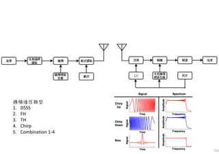
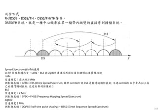
直接序列擴頻(DSSS)
直接用具有高速率的擴
頻碼序列在發端去擴展
信號的頻譜。
接收端, 用相同的擴頻
碼序列進行解擴, 把展
寬的擴頻信號還原成原
始資訊。
通常DSSS, PN碼的速率Rp
遠遠大於信碼速率Rm, 即
Rp>>Rm(也就是PN碼的寬
度Tp遠遠小於信碼的寬
度即Tp<<Tb), 這樣才能展
寬頻譜.
Gp = 10log10 Tb/Tp
通 常 carrier 頻 率 很 高
(GHz), Tc carrier週期很小,
有Tc<<Tp.
159.
159
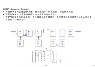
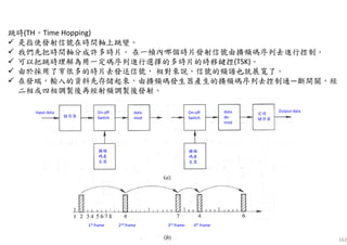
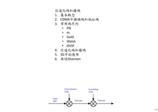
跳頻(FH, Frequency Hopping)
用擴頻碼序列去進行FSK調製,使載波頻率不斷地跳變,因此稱為跳頻。
簡單如2FSK, 只有兩個頻率, 分別代表傳號和空號。
而實際跳頻系統則有幾個、 幾十個甚至上千個頻率,由所傳資訊與擴頻碼的組合去進行選
擇控制, 不斷跳變。
Input data
擴頻
碼產
生器
data
mod
頻率
合成
器
RF
mod
RF產
生器
Mixer IF
BPF
data
de-
mod
Output data
擴頻
碼產
生器
頻率
合成
器
167
再談Shannon
由Shannon公式可以看出
1. 要增加系統的信息傳輸速率, 則要求增加信道容量,
增加信道容量的方法可以通過
•增加傳輸信號頻寬B or
• 增加信噪比S/N來實現(增加B比增加S/N更有效)
2. 信道容量C為常數時, 頻寬B與信噪比S/N可以互換
• 即可以通過增加頻寬B來降低系統對信噪比
S/N的要求(Transceiver好做)
• 也可通過增加信號功率, 降低信號的頻寬
• 這就為那些要求小信號頻寬的系統或對信號
功率要求嚴格的系統找到了一個減小頻寬或
降低功率的有效途徑
3. 當B增加到一定程度後, C不可能無限制增加(i.e. S和
N0一定時, C是有限的).
2
2
0
0
0
log 1 bit/s
log 1 bit/s
where is AWGN SSB PSD and
S
C B
N
S
B
N B
N
N N B
= ⋅ +
= ⋅ +
=
Shannon定理指出: 在高斯白噪聲信道中, 通信系統的最大信道容量為B為信號
頻寬, S為信號的平均功率, N為雜訊平均功率。
B, N0, S確定後, C即確定
Shannon第二定理知: 若信源(信息傳輸速率)R ≤ C(信道容量)
• 通過編碼, 信源的信息能以無限小的差錯機率通過信道傳輸
• 每隔十年演進一代的通信技術就是以速率作為最基本的目標
0
2
0
2 2
lim lim log 1
1
lim 1
1
lim log 1 l
1.44
og 1.44
B B
n
n
x
S
C B
N B
e
n
x
x
S
N
e
→∞ →∞
→∞
→∞
= ⋅ + =
= +
∴ + = ≈
∵
max
0
max
max
0 0 0 max
0
, ,
/ ,
sec
1
lim 1.44 ,
1.44
1
0.694
1.
1.6 d
4
B
4
b b
b
b
B
b
R R C B
J
E N E
bit
J bit
S E R
bi
E
t
ES S
R C
N N N
N
R→∞
= = → ∞
= ⋅
= = ∴ = =
= = = −
∵
信息傳輸速率的極限 當
信道要求的最小信躁比 為碼元能量
信道要求的最小信躁比
Called Shannon limit
168.
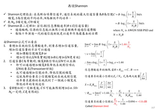
168Comparison of severalmodulation schemes at Pe = 10-5 symbol error probability
差錯機率
0
max
0
max
max
0 0 0 max
0
, ,
/ ,
sec
1
lim 1.44 ,
1.44
1
0.694
1.44
2 , 1
1
/
.6 dB
b b
b
b
B
e
b
b
E
N
R R C B
J
E N E
bit
J bit
S E R
bit
ES S
R C
N N N R
E
P f
N
T B
→∞
= = → ∞
= ⋅
= = ∴ = =
= = =
=
−
=
∵
信息傳輸速率的極限 當
信道要求的最小信躁比 為碼元能量
信道要求的最小信躁比
進制信息碼元寬度 信息帶寬
0
0
2 /
,
b
e
T
S E T
W N N W
E STW S W
P f f f
N N N B
=
=
= = =
進制信息功率
已擴頻信號帶寬 噪聲功率
169.
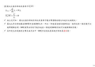
1 10 100
0
50
100
150
200
250
300
Bandwidth-limited
region
Ebn0ratio(dB)
Bandwidthutilization γ
power-limited
region
0.1 1 10
-10
-5
0
5
10
15
20
Bandwidth-limited
region
Ebn0ratio(dB)
Bandwidth utilization γ
power-limited
region
2
2 2
0
2
0
0 0
Def BW utilizat
log 1
log 1 log 1
log 1
2 1
min
ion,
.
b
b
b b
S
C BW
N
E RS
R C BW BW
N N BW
E
N
E E
N
R
B
N
W
γ
γ γ
γ
γ
= ⋅ +
⋅
≤ = ⋅ + = ⋅ +
⋅
≤ +
−
⇒ ≥ =
≡
⇒
1. ߛ < 1, Eb/N0 = const, N0固定Eb也固定. S = Eb × R, S ↑, R ↑.
2. ߛ > 1, min required Eb/N0 increases rapidly with ߛ, if R of
same order or larger than BW, if without increase
corresponding BW, S ↑↑↑, R ↑.
169
Zoom in
181
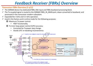
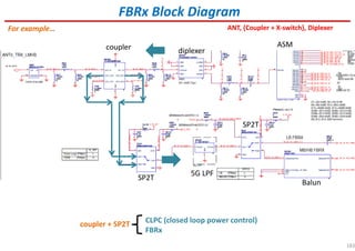
Feedback Receiver (FBRx)Overview
Transceiver FBRx Overview (1 of 2)
The SDR660 device has dedicated FBRx LNA input and FBRx baseband processing block.
The Tx-coupled signal is routed to the SDR660 FBRX_IN_MAIN port, down-converted to baseband, and
processed in the transceiver modem subsystem.
Expanded for 3 GHz and 5.5 GHz operation.
Used in the factory and in online mode for the following purposes:
Maximum Tx power control:
• PDET functionality.
Tx inner-loop power control (ILPC) accuracy:
• Corrected for Tx power step change.
• Avoids ILPC re-tweaking inconvenience.
182.
182
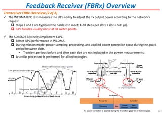
Feedback Receiver (FBRx)Overview
Transceiver FBRx Overview (2 of 2)
The WCDMA ILPC test measures the UE’s ability to adjust the Tx output power according to the network’s
request.
Steps E and F are typically the hardest to meet: 1 dB steps per slot (1 slot = 666 μs).
ILPC failures usually occur at PA switch points.
The SDR660 FBRx helps implement CLPC.
Better ILPC performance in WCDMA.
During mission mode: power sampling, processing, and applied power correction occur during the guard
period between slots.
• Transient periods before and after each slot are not included in the power measurements.
A similar procedure is performed for all technologies.
188
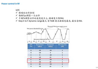
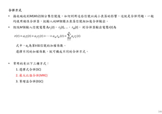
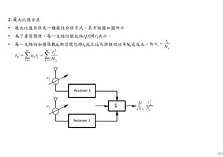
2. 最大比值合並
• 最大比值合併是一種最佳合併方式,其方框圖如圖所示
•為了書寫簡便,每一支路信號包絡rk(t)用rk表示。
• 每一支路的加權係數ak與信號包絡rk成正比而與雜訊功率Nk成反比,即
k
k
k
N
r
a =
2
1 1
M M
k
R k k
k k k
r
r a r
N= =
= =∑ ∑
Receiver 1
Receiver 1
191
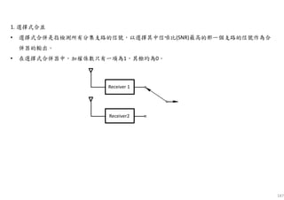
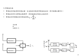
1. 選擇式合併的性能選擇式合併的性能選擇式合併的性能選擇式合併的性能
• 選擇式合併器的輸出信噪比,即當前選用的那個支路送入合併器的信噪比。
•設第k個支路的信號功率為r2
k/2,噪聲功率為Nk, 可得第k支路的信噪比為
• 通常,一支路的信噪比必須達到某一門限值γt,才能保證接收機輸出的話音品質(或誤碼率)達到要
求。
• 如果此信噪比因為衰落而低於這一門限,則認為這個支路的信號必須捨棄不用。
• 在選擇式合併的分集接收機中,只有全部M個支路的信噪比都達不到要求,才會出現通信中斷。
若第k個支路中γk<γt的概率為Pk(γk<γt),則在M個支路情況下中斷概率以PM(γS<γt)表示時,可得
2
2
k
k
k
r
N
γ =
1
( ) ( )
M
M S t k k t
k
P Pγ γ γ γ
=
≤ = ≤∏ 2k k tr N γ≤
22
/
0
( 2 ) ( ) 1
k t
k t k
N
N
k k k t k k kP r N p r dr e
γ γ σ
γ −
≤ = = −∫
由式可見,γk ≤ γt,即r2
k/2Nk ≤ γt,
因此
設rk的起伏服從瑞利分佈,即
可得
1
( ) ( 2 )
M
M S t k k k t
k
P P r Nγ γ γ
=
≤ = ≤∏
2 2
/(2 )
2
( ) k krk
k k
k
r
p r e σ
σ
−
=
192.
192
則
如果各支路的信號具有相同的方差,即
各支路的雜訊功率也相同,即 N1 =N2 = … = N
令平均信噪比為 ,則
由此可得M重選擇式分集的可通率為
由於(1-e-γt/γ0)的值小於1,因而在γt/γ0一定時,分集重數M增大,可通率T隨之增大。
2
/
1
( ) (1 )k t k
M
N
M S t
k
P e γ σ
γ γ −
=
≤ = −∏
2 2 2
1 2σ σ σ= = =⋯
2
0/ Nσ γ=
0/
( ) (1 )t M
M S tP e γ γ
γ γ −
≤ = −
0/
( ) 1 (1 )t M
M S tT P e γ γ
γ γ −
= > = − −
194
2. 最大比值合併的性能最大比值合併的性能最大比值合併的性能最大比值合併的性能
• 最大比值合併器輸出的信號包絡,即
•信躁比為
• 由於各支路信噪比為 即
• 代入上面可得
• 根據Cauchy–Schwarz inequality
• 利用上述關係式,代入得
∑∑ ==
==
M
k k
k
M
k
kkR
N
r
rar
1
2
1
2
1
2
1
( / 2)
M
k k
k
R M
k k
k
a r
a N
γ =
=
=
∑
∑
2k k kr N γ=
2
1
2
1
( )
M
k k k
k
R M
k k
k
a N
a N
γ
γ =
=
=
∑
∑
2
2
k
k
k
r
N
γ =
kkk
M
k
M
k
M
k
qNap
qppq
γ==
⋅
≤
∑∑∑ === 1
2
1
2
2
1
2
2
1 1 1
M M M
k k k k k k
k k k
a N a Nγ γ
= = =
⇒ ≤ ⋅
∑ ∑ ∑
2
1 1
2 1
1
( )( )
M M
k k k M
k k
R kM
k
k k
k
a N
a N
γ
γ γ= =
=
=
≤ =
∑ ∑
∑
∑
由上式可知由上式可知由上式可知由上式可知,,,,最大比值合併器輸出可能得到的最大信噪比最大比值合併器輸出可能得到的最大信噪比最大比值合併器輸出可能得到的最大信噪比最大比值合併器輸出可能得到的最大信噪比
為各支路信噪比之和為各支路信噪比之和為各支路信噪比之和為各支路信噪比之和,,,,即即即即
max
1
M
R k
k
γ γ
=
= ∑
203
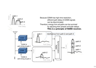
Because CDMA hashigh time-resolution,
different path delay of CDMA signals
can be discriminated.
Therefore, energy from all paths can be summed
by adjusting their phases and path delays.
This is a principle of RAKE receiver.
Path Delay
Power
path-1
path-2
path-3
CDMA
Receiver
CDMA
Receiver
•••
Synchronization
Adder
Path Delay
Power
CODE A
with timing of path-1
path-1
Power
path-1
path-2
path-3
Path Delay
Power
CODE A
with timing of path-2
path-2
interference from path-2 and path-3
•••
205
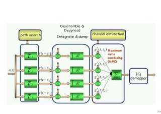
Delay
Rake finger processing
T
dt⋅∫
Σ
Received
signal
ToMRC
T
dt⋅∫( )if τ
Stored code sequence
(Case 1: same code in I and Q branches)
I branch
Q branch
I/Q
Output of finger: a complex signal value for each detected bit
Case 1: same code in I and Q branches
- for purpose of easy demonstration only
- no phase synchronization in Rake fingers
206.
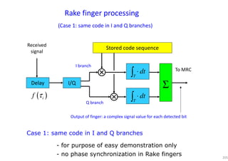
206
Delay
Rake finger processing
T
dt⋅∫
Receivedsignal
T
dt⋅∫
Stored I code sequence
(Case 2: different codes in I and Q branches)
I branch
Q branch
I/Q
Stored Q code sequence
iφ
To MRC for I
signal
To MRC for Q
signal
Required: phase
synchronization
( )if τ
Case 2: different codes in I and Q branches
- the real case in IS-95 and WCDMA
- phase synchronization in Rake fingers
208
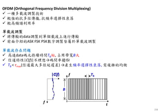
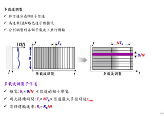
OFDM (Orthogonal FrequencyDivision Multiplexing)
一種多載波調製技術
較強的抗多徑傳播, 抗頻率選擇性衰落
較高頻譜利用率
單載波單載波單載波單載波調製調製調製調製
將傳輸的data調製到單個載波上進行傳輸
前面介紹的ASK FSK PSK數字調製皆屬於單載波調製
|C(f)
|
t
f
f
B
TB
單單單單載波載波載波載波存在存在存在存在問題問題問題問題
高速data碼元持續時間TB短, 占用帶寬B大
信道特性|C(f)|不理想→碼間串擾ISI
TB < τmax(信道最大多徑延遲差) →產生頻率選擇性衰落, 需複雜的均衡
|C(f)
|
209.
209
NTB
t
f
B/N
多載波調製子多載波調製子多載波調製子多載波調製子信信信信道道道道
頻寬: Bi =B/N < 信道的相干帶寬
碼元持續時間: Ti = NTB > 信道最大多徑時延τmax
資料傳輸速率: Ri = RB/N
|C(f)
|
t
f
f
B
TB
B
TB
多載波多載波多載波多載波調製調製調製調製
將信道分成N個子信道
高速串/並N路低速子數據流
分別調製到各個子載波上並行傳輸
單載波調製單載波調製單載波調製單載波調製 多載波調製多載波調製多載波調製多載波調製
211
表表表表達達達達式式式式表表表表達達達達式式式式
設OFDM系統中有N個子信道,每個子信道採用的子載波子載波子載波子載波為:
( ) cos(2) 0,1,2 , -1k k k kx t B f t k Nπ φ= + = ⋯
Where Bk 、fk、ϕk -分別為第k路子載波的振幅、頻率、初始相位;
Bk 受基帶碼元的調製。則此系統中的 N 路子信號之和為:
1 1
0 0
( ) ( ) cos(2 )
N N
k k k k
k k
e t x t B f tπ φ
− −
= =
= +∑ ∑=
可改寫成:
∑
−
=
+
=
1
0
2
B
N
k
tfj
k
kk
ete )(
)( ϕπ
Bk是一個複數, 為第k路子信道中的複輸入資料
212.
212
0
1
{cos[(2 ( )] cos[(2 ( ) ]} 0
2
BT
k i k i k i k if f t f f t dtπ φ φ π φ φ− + − + + + + =∫
即
正交條件正交條件正交條件正交條件正交條件正交條件正交條件正交條件
為了使這N路子信道信號在接收時能夠完全分離, 要求它們滿
足正交條件。在TB內, 任意兩個子載波都正交的條件是:
[ ] [ ]
( ) ( )
sin 2 ( ) sin 2 ( )
2 ( ) 2 ( )
sin sin
0
2 ( ) 2 ( )
k i B k i k i B k i
k i k i
k i k i
k i k i
f f T f f T
f f f f
f f f f
π φ φ π φ φ
π π
φ φ φ φ
π π
+ + + − + −
+ −
+ −
+ −
− =
+ −
積分結果為
0
cos(2 )cos(2 ) 0
BT
k k i if t f t dtπ ϕ π ϕ+ + =∫
213.
213
( ) and( )k i B k i Bf f T m f f T n+ = − =
Where m = 整數和n = 整數;並且ϕk和ϕi可以取任意值
( ) / 2 , ( ) / 2k B i Bf m n T f m n T= + = −
上式等於0的條件:
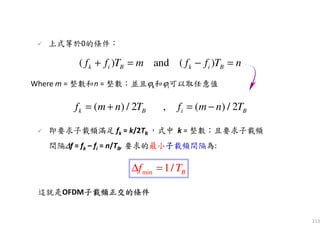
這就是OFDM子載頻正交的條件子載頻正交的條件子載頻正交的條件子載頻正交的條件
即要求子載頻滿足 fk = k/2TB ,式中 k = 整數;且要求子載頻
間隔∆∆∆∆f = fk – fi = n/TB, 要求的最小子子子子載頻間隔為:
min 1/ Bf T∆ =
217
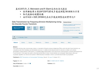
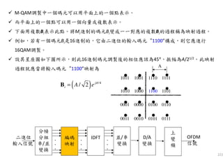
直到1971年, S. Weinsteinand P. Ebert這兩位老兄提出
• 採用離散傅立葉(IDFT/DFT)實現多載波調製/解調解決方案
• 取代複雜的硬體結構
• 由於VLSI + DSP, OFDM代表的多載波調製技術實用化!!
218.
218
OFDM的實現:以MQAM調製為例
複習DFT公式
設一個時間信號s(t)的抽樣函數為s(k),其中k = 0,1, 2, … , K– 1,
則s(k)的離散傅裡葉變換(DFT)定義為:
並且S(n)的逆離散傅裡葉變換(IDFT)為:
1
(2 / )
0
1
( ) ( )
K
j K nk
k
S n s k e
K
π
−
−
=
= ∑ )1,,2,1,0( −= Kn ⋯
∑
−
=
=
1
0
)/2(
)(
1
)(
K
n
nkKj
en
K
ks π
S )1,,2,1,0( −= Kk ⋯
223
用IDFT實現OFDM
1st 令OFDM的最低子載波頻率等於0,以滿足下式
右端第一項(即n =0時)的指數因數等於1。
為了得到所需的已調信號最終頻位置,可以用上變頻的方法將所得OFDM信號的頻譜
向上搬移到指定的高頻上。
∑
−
=
=
1
0
)/2(
)(
1
)(
K
n
nkKj
en
K
ks π
S )1,,2,1,0( −= Kk ⋯
分幀
分組
串/並
變換
編碼
映射
.
.
.
.
.
.
IDFT .
.
.
並/串
變換
D/A
變換
上
變
頻
OFDM
信號
二進位
輸入信號
224.
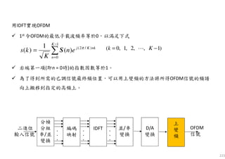
224
2nd 我們令K =2N,使IDFT的項數K等於子信道數目N的2倍,並用對稱性條件:
由N個並行複數碼元序列{Bi},(其中i = 0, 1, 2, …, N – 1),生成K=2N個等效的複數碼元序列
{Bn
′},(其中n = 0, 1, 2, …, 2N – 1),即令{Bn
′}中的元素等於:
這樣將生成的新碼元序列{Bn
′}作為S(n),代入IDFT公式,得到
)(*)1( kkK SS =−− )1,,2,1,0( −= Kk ⋯
*
1
1
0 0
1 2 1 0
, 1, 2, , 1
, , 1, 2, , 2 2
Re( )
Im( )
K n n
K n n
K N
n N
n N N N N
− −
− −
− −
′ = = −
′ = = + + −
′ =
′ ′= =
B B
B B
B B
B B B
⋯
⋯
∑
−
=
′=
1
0
)/2(1
)(
K
n
nkKj
ne
K
ks π
B )1,,2,1,0( −= Kk ⋯
分幀
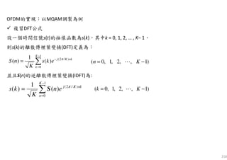
分組
串/並
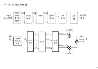
變換
編碼
映射
.
.
.
.
.
.
IDFT .
.
.
並/串
變換
D/A
變換
上
變
頻
OFDM
信號
二進位
輸入信號
225.
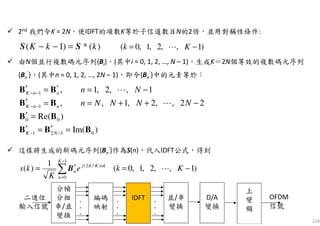
225
式中
相當於OFDM信號s(t)的抽樣值。
故s(t)可以表示為
子載波頻率fk = n/TB,(n= 0, 1, 2, … , N - 1)。
離散抽樣信號s(k)經過D/A變換後就得到上式的OFDM信號s(t)。
3rd 近一步克服ISI, 在OFDM相鄰碼元間加入保護間隔(CP)
( ) ( / )Bs k s kT K=
∑
−
=
′=
1
0
)/2(1
)(
K
n
nkKj
ne
K
ks π
B
1
(2 / )
0
1
( ) B
K
j T nt
n
n
s t e
K
π
−
=
′= ∑B (0 )Bt T≤ ≤
分幀
分組
串/並
變換
編碼
映射
.
.
.
.
.
.
IDFT .
.
.
並/串
變換
D/A
變換
上
變
頻
OFDM
信號
二進位
輸入信號


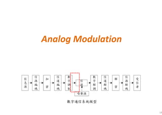
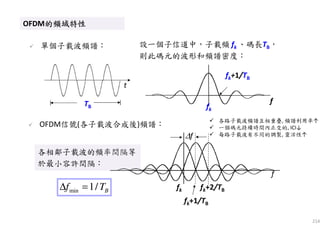
![15
BB signal
Carrier signal
RF signal
BB signal spectrum
RF signal spectrum
( ) coss t tω=
cos( ) cos( )
( ) ( )cos
2
c c
RF c
t t
s t s t t
ω ω ω ω
ω
− + +
= =
[ ]
2
( ) { ( )}
1
( ) { ( )cos } ( ) ( )
2
1 1
( )cos ( )cos ( ) ( ) ( )cos(2 )
2 2
RF c c c
RF c c c
S F s t
S F s t t S S
r t t s t t s t s t t
ω
ω ω ω ω ω ω
ω ω ω
=
= = − + +
= = +Demodulation →
LPF
Q: 同頻同相(相干解調) 難在…?
1 1
( )cos( ) ( )cos ( )cos(2 )
2 2
RF c cr t t s t s t tω φ φ ω φ+ = + +
相干解調相干解調相干解調相干解調
Modulation](https://image.slidesharecdn.com/wirelesscommshorttalk05312017final-170531084654/85/Wireless-Communication-short-talk-15-320.jpg)
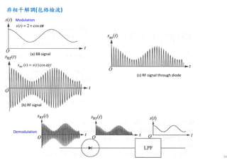
![33
Analog Modulation
Amplitude
Modulation
(linear)
Angle
Modulation
(nonlinear)
FM PM
角度調製一般式角度調製一般式角度調製一般式角度調製一般式
( ) cos[ ( ])m cs t A t tϕω= +
載波的振幅載波的振幅載波的振幅載波的振幅恒定恒定恒定恒定
[ωωωωct +ϕϕϕϕ(t)] –已已已已調信號的調信號的調信號的調信號的瞬時瞬時瞬時瞬時相位相位相位相位
ϕϕϕϕ(t)相對於相對於相對於相對於ωωωωct的的的的瞬時相位偏移瞬時相位偏移瞬時相位偏移瞬時相位偏移
[ ωωωωc + dϕϕϕϕ(t)/dt ] –已已已已調信號的瞬時調信號的瞬時調信號的瞬時調信號的瞬時角頻率角頻率角頻率角頻率
dϕϕϕϕ(t)/dt相對於相對於相對於相對於ωωωωc的的的的瞬時角頻偏瞬時角頻偏瞬時角頻偏瞬時角頻偏](https://image.slidesharecdn.com/wirelesscommshorttalk05312017final-170531084654/85/Wireless-Communication-short-talk-33-320.jpg)
![34
Kf =rad/(s•V)
Kp=rad/VPM:
FM::::
( ) ( )pKt m tϕ =
( )
( )f
d t
m t
dt
K
ϕ
=
( ) cos[ ( ])m cs t A t tϕω= +
FM是相位偏移隨m(t)的積分呈線性變化
如果預先不知道調製信號m(t)的具體形式, 則無法
判斷已調信號是調相信號還是調頻信號
PM是相位偏移隨調製信號m(t)線性變化](https://image.slidesharecdn.com/wirelesscommshorttalk05312017final-170531084654/85/Wireless-Communication-short-talk-34-320.jpg)
![35
單音調制單音調制單音調制單音調制FM與與與與PM
( ) cos[ ( )]
( ) cos[ cos ] cos[ cos ]
,
PM c p
PM c p
p
c
p
m
m
m p m
s t A t K m t
s t A t K A t A t m t
m K A
ω
ω ω ω ω
= +
= +
=
= +
用它對載波進行相位調製
調相指數 表示最大的相位偏移
( ) cos cos2
( ) cos[ ( ) ]
( ) cos[ cos ] cos[ sin ]
m m m m
FM c f
FM c f m m c f m
f m
f
m m m
f m
f m
m t A t A f t
s t A t K m d
s t A t K A d A t m t
K A f
m
f
K A
f m f
ω π
ω τ τ
ω ω τ τ ω ω
ω
ω ω
ω
= =
= +
= + = +
∆ ∆
= = =
∆ =
∆ = ⋅
∫
∫
用它對載波進行頻率調製
調頻指數,表示最大的相位偏移
最大角頻偏
最大頻偏
( ) cos cos2m m m mm t A t A f tω π= =
設調製信號為單一頻率的正弦波
t
( )m t
t
( )m t
t
( )tω
t
( )tω
cω
( )PMs t
t
( )FMs t
t
cω](https://image.slidesharecdn.com/wirelesscommshorttalk05312017final-170531084654/85/Wireless-Communication-short-talk-35-320.jpg)
![38
Phase Locked Loop (PLL)
相干相干相干相干解調最重要的元件之一解調最重要的元件之一解調最重要的元件之一解調最重要的元件之一
假設PLL input
output
{ }
( ) cos(2 )
( ) sin(2 )
1
( ) ( ) ( ) sin[2 ( ) ] sin[2 ( ) ]
2
LPF negative feedback " " VCO
1
( ) sin[2 ( ) ]
2
if then VCO tracking input signa
c
c
c c c c
c c c
c c
s t f t
c t f t
e t s t c t f f t f f t
u t f f t
f f
π φ
π φ
π φ φ π φ φ
π φ φ
= +
′ ′= +
′ ′ ′ ′= = − + − + + + +
→ → − →
−
′ ′= − + −
′ ≠
作為 控制電壓
l freq. until
1
if then ( ) sin[ ]
2
VCO ,
1
( ) [ ]
2
c c
c c c
c
f f
f f u t
u t
φ φ
φ φ φ φ
′ =
′ ′= = −
′ ′≈ − ⇒ ≈
控制靈敏度很高 只需很小的相差就可維持頻率鎖定
( )s t
( )c t
0
0
( ) 2 ( )
( ) ( ) 2 ( )c
t f t t
d
t t f Ku t
dt
θ π φ
ω θ π
= +
= = +
1. 表達式
2. 擾動行為
• (某種擾動原
因使φ’增大)
↑↓
↓↓↓
↓ ↓](https://image.slidesharecdn.com/wirelesscommshorttalk05312017final-170531084654/85/Wireless-Communication-short-talk-38-320.jpg)
![( )y t
( )C ω
{ }na
( )d t
48
Digital Modulation
( ) ( )
( ) ( ) ( ) ( )
1
( ) ( )
2
( ) ( ) ( ) ( )
1
( ) ( )
2
n s
n
T n T s
n
j t
T T
T R
j t
d t a t nT
s t d t g t a g t nT
g t G e d
H G C G
h t H e d
ω
ω
δ
ω ω
π
ω ω ω ω
ω ω
π
∞
=−∞
∞
=−∞
∞
−∞
∞
−∞
= −
= ∗ = −
=
=
=
∑
∑
∫
∫
s(t)
[ ]0 0 0 0
( ) ( ) ( ) ( ) ( ) ( )
( ) ( ) ( ) ( )
R n S R
n
s k n s R s
n k
r t d t h t n t a h t nT n t
r kT t a h t a h k n T t n kT t
∞
=−∞
≠
= ∗ + = − +
+ = + − + + +
∑
∑
r(t) 0( )sr kT t+⊕
{ }na′0,1,0,1 or -1,1,-1,1
對應的BB signal
gT(t): impulse response
分析前先把model建好
nR(t)是加性雜訊n(t)經過接
收濾波器後輸出的雜訊
為了確定第k個碼元 ak 的取值, 首先應
在t = kTs + t0 時刻上對r(t)進行抽樣, 以確
定r(t)在該樣點上的值](https://image.slidesharecdn.com/wirelesscommshorttalk05312017final-170531084654/85/Wireless-Communication-short-talk-48-320.jpg)
![49
第一項akh(t0)是第k個接收碼元波形的抽樣值, 它是確定ak的依據.
第二項(Σ項)是除第k個碼元以外的其它碼元波形在第k個抽樣時刻上的總和(代數和), 它對當
前碼元ak的判決起著干擾的作用, 所以稱之為碼間串擾值(ISI).
由於ak是以概率出現的, 故ISI通常是一個隨機變數.
第三項nR(kTB + t0)是輸出雜訊在抽樣瞬間的值, 它是一種隨機干擾, 也會影響對第k個碼元的正
確判決.
[ ]0 0 0 0( ) ( ) ( ) ( )s k n s R s
n k
r kT t a h t a h k n T t n kT t
≠
+ = + − + + +∑
Digital Modulation
ISI](https://image.slidesharecdn.com/wirelesscommshorttalk05312017final-170531084654/85/Wireless-Communication-short-talk-49-320.jpg)
![50
( )h t
0t 0sT t+
( )h t
0t 02 sT t+0sT t+
[ ]0(ISI )n s
n k
a h k n T t
≠
= − +∑
( ) 0+ =0n s
n k
a h k n T t
≠
− ∑
若能使若能使若能使若能使:
, 則無則無則無則無ISI
怎麼做怎麼做怎麼做怎麼做????
做不到做不到做不到做不到 關注抽樣時刻關注抽樣時刻關注抽樣時刻關注抽樣時刻
等等等等Ts的零的零的零的零點點點點
由於an是隨機的,要想通過各項相互抵消使碼間串擾為0是不行的
這就需要對h(t)的波形提出要求。
若讓h [(k-n)Ts +t0] 在Ts+ t0 、2Ts +t0等後面碼元抽樣判決時刻上正好為0,就能消除碼間串擾
這就是消除碼間串擾的基本思想](https://image.slidesharecdn.com/wirelesscommshorttalk05312017final-170531084654/85/Wireless-Communication-short-talk-50-320.jpg)
![54
Digital Modulation
raised-cosine filter minimize ISI
(1 )
, 0
(1 ) (1 )
( ) [1 sin ( )],
2 2
(1 )
0,
S
S
S S
S S S
S
T
T
T T
H
T T T
T
α π
ω
π α π α π
ω ω ω
α
α π
ω
−
≤ <
− +
= + − ≤ <
+
≥
( ) 2 2 2
sin / cos /
/ 1 4 /
S S
S S
t T t T
h t
t T t T
π απ
π α
= ⋅
−
FT
/ Nf fα ∆≡
引入滾降係數
描述滾降程度
( )0 ~1
1
2
N
B N
B
f
f
R f
T
α ∆
=
= =
(1 )N NB f f fα∆= + = +](https://image.slidesharecdn.com/wirelesscommshorttalk05312017final-170531084654/85/Wireless-Communication-short-talk-54-320.jpg)
![55
(1 )
, 0
(1 ) (1 )
( ) [1 sin ( )],
2 2
(1 )
0,
S
S
S S
S S S
S
T
T
T T
H
T T T
T
α π
ω
π α π α π
ω ω ω
α
α π
ω
−
≤ <
− +
= + − ≤ <
+
≥
( ) 2 2 2
sin / cos /
/ 1 4 /
S S
S S
t T t T
h t
t T t T
π απ
π α
= ⋅
−
FT
/ Nf fα ∆≡
Digital Modulation
root-raised-cosine (RRC) filter
實際應用中1個在Tx, 1個在Rx, raised-cosine RRC RRC= ⋅
√ ̄
√ ̄ ̄ ̄ ̄ ̄ ̄
余弦滾降濾波器特點
1. 特性易實現
2. Response曲線拖尾收斂快, 擺幅較小
BUT代價
1. BW↑
2. 頻帶利用率η↓](https://image.slidesharecdn.com/wirelesscommshorttalk05312017final-170531084654/85/Wireless-Communication-short-talk-55-320.jpg)
![58
時域均衡時域均衡時域均衡時域均衡 → ISI↓
( )H ω′
有有有有 ISI
ݔݔݔݔ()ݐ
( )H ω ( )T ω
無無無無 ISI
ݕݕݕݕ()ݐ有有有有誤差誤差誤差誤差
( ) ( ) ( ) ( )if equalizer
ISI
then ( ) ISIy t
HT THω ωωω =′∋插入
滿足無 的頻域條件
在抽樣時刻上無
( )
1
,
2 2
) ) ,
2 /
,
( ) ( )
(
( )
( )
( ) (
2
( )
( ) [ ] ( )
22
2
(
(
)
)
B
B
i B
B
i B B B
B
B
B
i B
jnT
n T n B
n n
jnB B
n
i B
B
T
T
i i
T
T T T
T
T
i TH
T
C e
i
T
T
T
T
h t F C t nT
T T
C e
i
H
T
H
H
H
T
T
H
T ω
ω
ω
ω
π
ω
π π π
ω
ω
ω
π
ω
π
π
ω
π
ω
δ
ω
ω
ω
π
ω
π
ω
ω
∞ ∞
− −
=−∞ =−∞
+
′ = ≤
+ ⋅ + = ≤
= ≤
+
= ⇔ = = −
=
+
=′
∑
∑
∑
∑ ∑
∑
帶入
是 為週期的函數
BB
B
TT
T
d
π
π ω−∫
由hT(t)構造出equalizer的結構: 橫向濾波器
( ) ( )T n B
n
h t C t nTδ= −∑](https://image.slidesharecdn.com/wirelesscommshorttalk05312017final-170531084654/85/Wireless-Communication-short-talk-58-320.jpg)
![65
多進制數位調製原理多進制數位調製原理多進制數位調製原理多進制數位調製原理
2進制: 每個 symbol 只攜帶 1 bit 信息
M log2M bit
Rb = bit rate = bps = [bit/sec]
RB = symbol rate
= #symbol/sec = [Baud]
B
b
b
R Baud
B Hz
R bit
B s Hz
η
η
=
= ⋅
2logb BR R M=
Rb 固定, 增加進制數M↑, 可降低RB↓
減少信號BW, 節省頻率資源
RB 固定, 增加進制數M↑, 可增大Rb↑
在相同BW內傳輸更多bit, ηb↑
目的: 就是為了提高信道的頻帶利用率!!
代價:
• BER↑(判決範圍減小), 系統複雜
• 若要保證一定的BER, SNR↑, 發射功率增大, 耗能…](https://image.slidesharecdn.com/wirelesscommshorttalk05312017final-170531084654/85/Wireless-Communication-short-talk-65-320.jpg)
![76
多進制數位調製原理多進制數位調製原理多進制數位調製原理多進制數位調製原理
2進制: 每個 symbol 只攜帶 1 bit 信息
M log2M bit
Rb = bit rate = bps = [bit/sec]
RB = symbol rate
= #symbol/sec = [Baud]
B
b
b
R Baud
B Hz
R bit
B s Hz
η
η
=
= ⋅
2logb BR R M=
Rb 固定, 增加進制數M↑, 可降低RB↓
減少信號BW, 節省頻率資源
RB 固定, 增加進制數M↑, 可增大Rb↑
在相同BW內傳輸更多bit, ηb↑
目的: 就是為了提高信道的頻帶利用率!!
代價:
• BER↑(判決範圍減小), 系統複雜
• 若要保證一定的BER, SNR↑, 發射功率增大, 耗能…](https://image.slidesharecdn.com/wirelesscommshorttalk05312017final-170531084654/85/Wireless-Communication-short-talk-76-320.jpg)
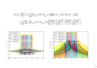
![81
恆包絡恆包絡恆包絡恆包絡 非恆包絡非恆包絡非恆包絡非恆包絡
Re[BB signal]
Im[BB signal]
Re[BB signal]
Im[BB signal]
RF signal RF signal
Pulse shaping採用矩形 4QAM Pulse shaping採用α = 0.5 raised cosine 4QAM](https://image.slidesharecdn.com/wirelesscommshorttalk05312017final-170531084654/85/Wireless-Communication-short-talk-81-320.jpg)

![10[ ] 174 10logSensitivity dBm BW loss RxNF C N= − + + + +
Technology GSM CDMA WCDMA TD-SCDMA LTE
BW [MHz] 0.2 1.23 3.84 1.28 9
C/N [dB] 4.75 -2 -9.5 -5.5 -1
RxNF [dB] 2.3-3.5 2.3-3 2.3-3 2.3-3 2.3-3
loss = total loss before LNA.
RxNF = receiver noise figure (ex: WTR3925)
80-NH379-121
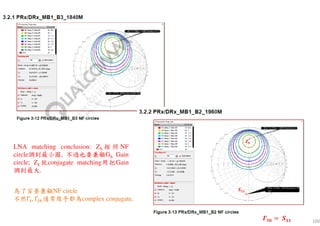
80-NH379-42
32 4
1
1 1 2 1 2 3
11 1
...total
FF F
F F
G G G G G G
−− −
= + + + +
1 2 31 1 2
1 2 3 4
1 1
...
3 3 3 3 3total
G G GG G G
IIP IIP IIP IIP IIP
= + + + +
我們已知 用火XD
102](https://image.slidesharecdn.com/wirelesscommshorttalk05312017final-170531084654/85/Wireless-Communication-short-talk-102-320.jpg)
![Type Trace ASM iLNA others
Stage Stage1 Stage2 Stage3 Stage4
NF [dB] 3 1 0.85 4
Gain [dB] -3 -1 15 -4
NF 2 1.26 1.22 2.51
Gain 0.5 0.79 31.62 0.4
10
1.26 1 1.22 1 2.51 1
2 3.19
0.5 0.5 0.79 0.5 0.79 31.62
10log (3.19) 5.04 [dB].
total
total
F
F
− − −
= + + + ≈
× × ×
= =
我們先假設一種情況 w/o eLNA
w/o eLNA
103](https://image.slidesharecdn.com/wirelesscommshorttalk05312017final-170531084654/85/Wireless-Communication-short-talk-103-320.jpg)
![Type ASM eLNA Trace iLNA others
Stage Stage1 Stage2 Stage3 Stage4 Stage5
NF [dB] 1 0.85 3 0.85 4
Gain [dB] -1 15 -3 15 -4
NF 1.26 1.22 2 1.22 2.51
Gain 0.79 31.62 0.5 31.62 0.4
10
1.22 1 2 1 1.22 1 2.51 1
1.26 1.59
0.79 0.79 31.62 0.79 31.62 0.5 0.79 31.62 0.5 31.62
10log (1.59) 2.02 [dB].
total
total
F
F
− − − −
= + + + + ≈
× × × × × ×
= =
比較最好的情況w/ eLNA
w/ eLNA
104](https://image.slidesharecdn.com/wirelesscommshorttalk05312017final-170531084654/85/Wireless-Communication-short-talk-104-320.jpg)
![代入理論公式太麻煩, 看能不能省去甚麼…
我們發現, LNA後方Stage會因分母有LNA的Gain, 其值會變很小因此省略計算
10
1.26 1 1.22 1 2.51 1
2 3.08
0.5 0.5 0.79 0.5 0.79 31.62
10log (3.08) 4.88 [dB].
total
total
F
F
− − −
= + + + ≈
× × ×
= =
10
1.22 1 2 1 1.22 1 2.51 1
1.26 1.54
0.79 0.79 31.62 0.79 31.62 0.5 0.79 31.62 0.5 31.62
10log (1.54) 1.88 [dB].
total
total
F
F
− − − −
= + + + + ≈
× × × × × ×
= =
做個table比較一下
NF 理論 NF 化簡
w/o eLNA 5.04 dB 4.88 dB
w/ eLNA 2.02 dB 1.88 dB
105](https://image.slidesharecdn.com/wirelesscommshorttalk05312017final-170531084654/85/Wireless-Communication-short-talk-105-320.jpg)
![化簡公式還要除, 還是覺得有點麻煩…看能不能更直觀 !!
直接將LNA input Stage的NF總和 [dB], 與從天線下來遇到的第一顆LNA自身的NF [dB], 兩個相加
NFtot [dB] = LNA pre-loss [dB] + LNA NF [dB]
再做個table比較一下
NF 理論 NF 化簡 NF 直觀
w/o eLNA 5.04 dB 4.88 dB 4.85 dB
w/ eLNA 2.02 dB 1.88 dB 1.85 dB
w/o eLNA
w/ eLNA
差不多, 計算方便, 又直觀
But 與理論有些微誤差.
106](https://image.slidesharecdn.com/wirelesscommshorttalk05312017final-170531084654/85/Wireless-Communication-short-talk-106-320.jpg)
![LTE B2 FE ASM Duplexer LNA Rx SAW DPDT Trace loss Loss before WTR Rx NF Rx BW CN Sensitivity
Typ 1.24 0.68 1.9 0.4 0.5 4.72 2.3 9 -1 -98.44
Max 1.62 0.83 3.5 0.4 0.8 7.15 3 9 -1 -95.31
For SXMX
LNA都先給他thru (w/o eLNA), 計算sensitivity
WCDMA B2 FE ASM Duplexer LNA Rx SAW DPDT Trace loss Loss before WTR Rx NF Rx BW CN Sensitivity
Typ 1.24 0.68 1.9 0.4 0.5 4.72 2.3 3.84 -9.5 -110.64
Max 1.62 0.83 3.5 0.4 0.8 7.15 3 3.84 -9.5 -107.51
BC1 FE ASM Duplexer LNA Rx SAW DPDT Trace loss Loss before WTR Rx NF Rx BW CN Sensitivity
Typ 1.24 0.68 1.9 0.4 0.5 4.72 2.3 1.23 -2 -108.08
Max 1.62 0.83 3.5 0.4 0.8 7.15 3 1.23 -2 -104.95
For SXMX
掛LNA (w/ eLNA), 計算sensitivity
由上頁知, NFtot [dB] = LNA pre-loss [dB] + LNA NF [dB]
Datasheet Infineon B2 LNA NF = 0.6-1.2, 再來我們忽略 RxSAW 與 DPDT 的NF.
LTE B2 FE ASM Duplexer LNA Rx SAW DPDT Trace loss Loss before WTR Rx NF Rx BW CN Sensitivity
Typ 1.24 0.68 1.9 0.6 0.5 4.92 2.3 9 -1 -98.24
Max 1.62 0.83 3.5 1.2 0.8 7.95 3 9 -1 -94.51
WCDMA B2 FE ASM Duplexer LNA Rx SAW DPDT Trace loss Loss before WTR Rx NF Rx BW CN Sensitivity
Typ 1.24 0.68 1.9 0.6 0.5 4.92 2.3 3.84 -9.5 -110.44
Max 1.62 0.83 3.5 1.2 0.8 7.95 3 3.84 -9.5 -106.71
BC1 FE ASM Duplexer LNA Rx SAW DPDT Trace loss Loss before WTR Rx NF Rx BW CN Sensitivity
Typ 1.24 0.68 1.9 0.6 0.5 4.92 2.3 1.23 -2 -107.88
Max 1.62 0.83 3.5 1.2 0.8 7.95 3 1.23 -2 -104.15
所以LNA掛WTR附近是沒有作用的.
107](https://image.slidesharecdn.com/wirelesscommshorttalk05312017final-170531084654/85/Wireless-Communication-short-talk-107-320.jpg)

![116
0
( )s t
tTB-TB
( )h t
0 tt0t0 -TB
因此, t0 ≥ TB
通常取 t0 = TB
0 0( ) ( ) [ ( )]h t s t t s t t= − = − −
問題: t0 = ????
鏡像鏡像鏡像鏡像及右移右移右移右移
圖解::::
這時 h(t) = s(TB-t)](https://image.slidesharecdn.com/wirelesscommshorttalk05312017final-170531084654/85/Wireless-Communication-short-talk-116-320.jpg)
![117
o ( ) ( ) ( ) ( ) ( )s t s t h t s ht dττ τ
∞
−∞
= ∗ = −∫
0) )( (ks ts t dτ ττ
∞
−∞
−= −∫
0 0( ) ( ) ( )k s x s x t t dx kR t t
∞
−∞
= + − = −∫
k=1 時
0( ) ( )os t R t t= −
t =t0 時
2
-0max[ ( )] ( ) ( ) ( )0o os t s R s Et tt d
∞
∞
= = = =∫
匹配濾波器匹配濾波器匹配濾波器匹配濾波器的的的的輸出信號輸出信號輸出信號輸出信號— so(t)
匹配匹配匹配匹配濾波器濾波器濾波器濾波器可看成是一個計算輸入信號自相關函數的相關器可看成是一個計算輸入信號自相關函數的相關器可看成是一個計算輸入信號自相關函數的相關器可看成是一個計算輸入信號自相關函數的相關器!!](https://image.slidesharecdn.com/wirelesscommshorttalk05312017final-170531084654/85/Wireless-Communication-short-talk-117-320.jpg)
![122
Channels
EM Wave在空氣中傳播的衰減在無線信道中分成:
• Slow fading (coherence time > delay time)
• Fast fading (coherence time << delay time)
Fast fading:
• Doppler effect
multipath多徑效應多徑效應多徑效應多徑效應
• 同相
• 反相: 移動λ /4, 相位+ - π/2
• 3G: 2GHz, λ~15 cm, λ /4 ~ 4 cm
• 人步速 = 1 m/s, 信道變化頻率 = 25次
• 10m/s, 信道變化頻率 = 250次
• 變化速度相對於陰影衰落是很快的 叫快衰落
(1 )
( ) cos[(1 )2 ] cos[(1 )2 ]
2cos(2 )cos(2 )
r s
s s
s s
v
f f
c
v v
r t f t f t
c c
v
f t f t
c
π π
π π
= +
= + + −
=
Doppler shift
1
coherent
Doppler
T
f
∝
∆
時間選擇性衰落(快衰落)
coherent Ɵme → 信號保持不變的時間](https://image.slidesharecdn.com/wirelesscommshorttalk05312017final-170531084654/85/Wireless-Communication-short-talk-122-320.jpg)
![123
0( ) ( )
( ) ( ) ( )
( ) ( )
[ ] ( )
( )
( )
o
o
i i
i
f c t
r t s t
s t s t s t
t
S SC
n
ω ωω
= +
= = ∗
=
( )H Kω = dtωωϕ =)( dt
d
d
==
ω
ωϕ
ωτ
)(
)(⇒⇒⇒⇒
無失真傳輸理想信道無失真傳輸理想信道無失真傳輸理想信道無失真傳輸理想信道
幅頻特性 相頻特性 Group delay特性
o ( ) ( )ds t K s t t= −
( ) dj t
H eK ω
ω −
= ( ) ( )dh t K t tδ= −
固定的遲延
固定的衰減
這種情況稱為無失真傳輸這種情況稱為無失真傳輸
若輸入信號為s(t),則理想恒參信道的輸出:
input output](https://image.slidesharecdn.com/wirelesscommshorttalk05312017final-170531084654/85/Wireless-Communication-short-talk-123-320.jpg)
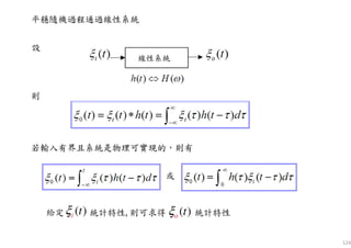
![輸入過程輸入過程輸入過程輸入過程 輸出過程輸出過程輸出過程輸出過程
機率分布 平穩平穩平穩平穩、、、、高斯高斯高斯高斯 平穩平穩平穩平穩、、、、高斯高斯高斯高斯
均值 常數常數常數常數 常數常數常數常數
PSD
ACF
125
[ ( )]iE t aξ = [ ( )] (0)oE t a Hξ = ⋅
( )iP f
( ) ( )i iR P fτ ⇔ ( ) ( )o oR P fτ ⇔
是線性系統的直流增益;
2
( )H f∫
∞
=
0
)()0( dtthH
o ( )tξ( )i tξ
是功率增益
2
( ) ( ) ( )o iP f H f P f=
P.S. 廣義平穩
均值與時間t無關
相關函數僅與τ有關](https://image.slidesharecdn.com/wirelesscommshorttalk05312017final-170531084654/85/Wireless-Communication-short-talk-125-320.jpg)
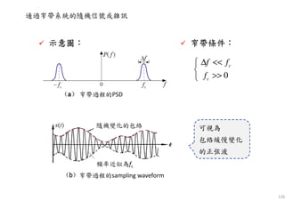
![127
運算式運算式運算式運算式::::
( ) cos[ ] , ( )( ) ( 0)ct t aa t t tξξ ξϕξ ω= + ≥
—包絡相位形式包絡相位形式包絡相位形式包絡相位形式
( ) ( )( ) cos sinc s cc t tt t tξ ωξ ξ ω= − —同相正交形式同相正交形式同相正交形式同相正交形式
隨機包絡隨機包絡隨機包絡隨機包絡 隨機相位隨機相位隨機相位隨機相位
同相分量同相分量同相分量同相分量 正交分量正交分量正交分量正交分量
兩者關係兩者關係兩者關係兩者關係::::
( )tξ](https://image.slidesharecdn.com/wirelesscommshorttalk05312017final-170531084654/85/Wireless-Communication-short-talk-127-320.jpg)
![132
( ) cos ctAs t ω=
[ ] [ ]
[ ]
[ ]
[ ]
1 1 2 2
1
1
( ) ( )cos ( ) ( )cos ( )
( ) ( )
( ) ( )
( )cos ( )
cos
cos
c c
n c n
n
c
i
n
c
i
i i
i i
r t a t t t a t t t
a t t t
t
t
a t t
a t t
ω τ ω τ
ω τ
ω τ
ϕω
=
=
= − + −
+ −
= −
= +
∑
∑
⋯
multipath多多多多徑效應徑效應徑效應徑效應
經過n條路徑條路徑條路徑條路徑傳播(各路徑有時變時變時變時變的衰落衰落衰落衰落和時延時延時延時延))))
— 多徑傳播的影響
)()( tt ici τωϕ −= )()( tt ici τωϕ −=
傳輸時延
則接收信號接收信號接收信號接收信號為
設發送發送發送發送信號為
幅度恒定
頻率單一
第i條路徑
接收信號振幅
(時變時變時變時變的衰落衰落衰落衰落)](https://image.slidesharecdn.com/wirelesscommshorttalk05312017final-170531084654/85/Wireless-Communication-short-talk-132-320.jpg)
![133
根據概率論中心極限定理:當 n
足夠大時,x(t)和y(t) 趨於正態分佈。
∑=
=
n
i
ii tatX
1
cos)()( ϕ
∑=
=
n
i
ii tatY
1
sin)()( ϕ
同相 ~ 正交形式
包絡 ~ 相位形式
瑞利瑞利瑞利瑞利
分佈分佈分佈分佈
均勻均勻均勻均勻
分佈分佈分佈分佈
[ ]cos( ) ( )cV t t tω ϕ= +
1 1
( ) ( )cos cos ( )sin sin
( )cos ( )sin
n n
i i c i i c
i i
c c
r t a t t a t t
X t t Y t t
ϕ ω ϕ ω
ω ω
= =
= −
= −
∑ ∑
包絡相位
隨機緩變的
窄帶信號](https://image.slidesharecdn.com/wirelesscommshorttalk05312017final-170531084654/85/Wireless-Communication-short-talk-133-320.jpg)
 co (s( ) )cr t V t t tω ϕ= +( ) cos ctAs t ω=
緩慢變化的包絡
結論結論結論結論
Multipath傳播使信號產生Rayleigh fading
Multipath傳播引起frequency spread
Multipath傳播引起數字信號ISI](https://image.slidesharecdn.com/wirelesscommshorttalk05312017final-170531084654/85/Wireless-Communication-short-talk-134-320.jpg)
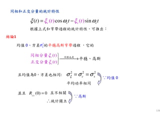
![149
Walsh碼碼碼碼
正交序列, 互相關函數 = 0
可由Hadamard matrix(+1 and -1的正交方陣)產生
• Hadamard matrix為對稱矩陣: HT = H
• H-1 = H/N, N = 2n order of Hn.
任兩個序列互相正交, Rab(0) = 0叫Walsh序列.
0
1 1
1 1
1
1 1
2
1 1
[1]
1 1
1 1
1 1 1 1
1 1 1 1
1 1 1 1
1 1 1 1
n n
n
n n
H
H H
H
H H
H
H H
H
H H
− −
− −
=
= −
= −
− − = = − − −
− − ](https://image.slidesharecdn.com/wirelesscommshorttalk05312017final-170531084654/85/Wireless-Communication-short-talk-149-320.jpg)


![212
0
1
{cos[(2 ( ) ] cos[(2 ( ) ]} 0
2
BT
k i k i k i k if f t f f t dtπ φ φ π φ φ− + − + + + + =∫
即
正交條件正交條件正交條件正交條件正交條件正交條件正交條件正交條件
為了使這N路子信道信號在接收時能夠完全分離, 要求它們滿
足正交條件。在TB內, 任意兩個子載波都正交的條件是:
[ ] [ ]
( ) ( )
sin 2 ( ) sin 2 ( )
2 ( ) 2 ( )
sin sin
0
2 ( ) 2 ( )
k i B k i k i B k i
k i k i
k i k i
k i k i
f f T f f T
f f f f
f f f f
π φ φ π φ φ
π π
φ φ φ φ
π π
+ + + − + −
+ −
+ −
+ −
− =
+ −
積分結果為
0
cos(2 )cos(2 ) 0
BT
k k i if t f t dtπ ϕ π ϕ+ + =∫](https://image.slidesharecdn.com/wirelesscommshorttalk05312017final-170531084654/85/Wireless-Communication-short-talk-212-320.jpg)


![RF Circuit Design - [Ch4-2] LNA, PA, and Broadband Amplifier](https://cdn.slidesharecdn.com/ss_thumbnails/ch4-2-150613064410-lva1-app6891-thumbnail.jpg?width=640&height=640&fit=bounds)


![射頻電子 - [實驗第四章] 微波濾波器與射頻多工器設計](https://cdn.slidesharecdn.com/ss_thumbnails/e4-150613065110-lva1-app6892-thumbnail.jpg?width=640&height=640&fit=bounds)


![射頻電子 - [實驗第三章] 濾波器設計](https://cdn.slidesharecdn.com/ss_thumbnails/e3-150613065109-lva1-app6891-thumbnail.jpg?width=640&height=640&fit=bounds)


![射頻電子 - [第五章] 射頻放大器設計](https://cdn.slidesharecdn.com/ss_thumbnails/ch5-150613065105-lva1-app6892-thumbnail.jpg?width=640&height=640&fit=bounds)
![射頻電子實驗手冊 - [實驗8] 低雜訊放大器模擬](https://cdn.slidesharecdn.com/ss_thumbnails/simlab8-150613072425-lva1-app6891-thumbnail.jpg?width=640&height=640&fit=bounds)


![射頻電子實驗手冊 - [實驗7] 射頻放大器模擬](https://cdn.slidesharecdn.com/ss_thumbnails/simlab7-150613072420-lva1-app6892-thumbnail.jpg?width=640&height=640&fit=bounds)


![電路學 - [第六章] 二階RLC電路](https://cdn.slidesharecdn.com/ss_thumbnails/circuitch6-150613063009-lva1-app6892-thumbnail.jpg?width=640&height=640&fit=bounds)