Download to read offline
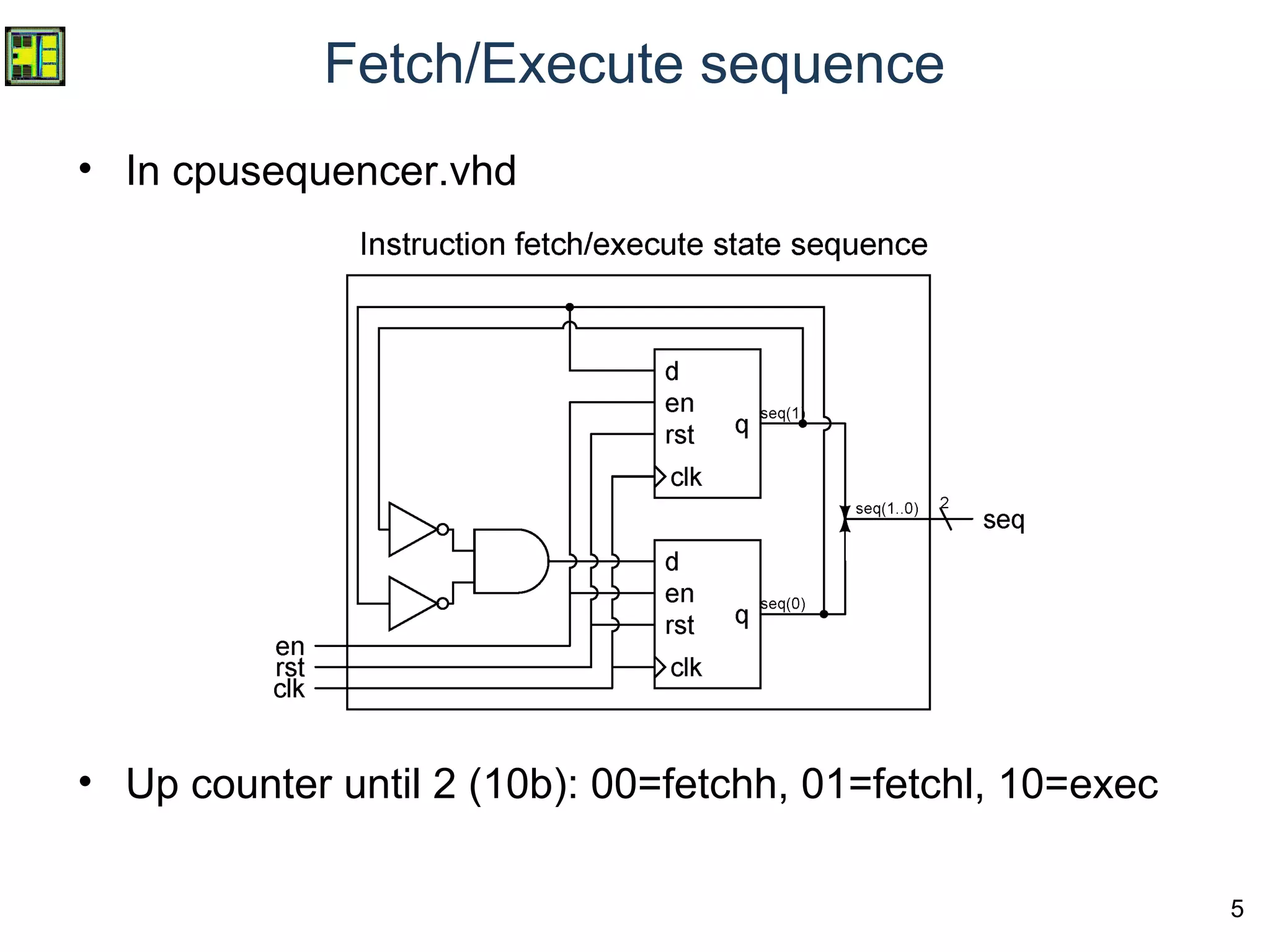
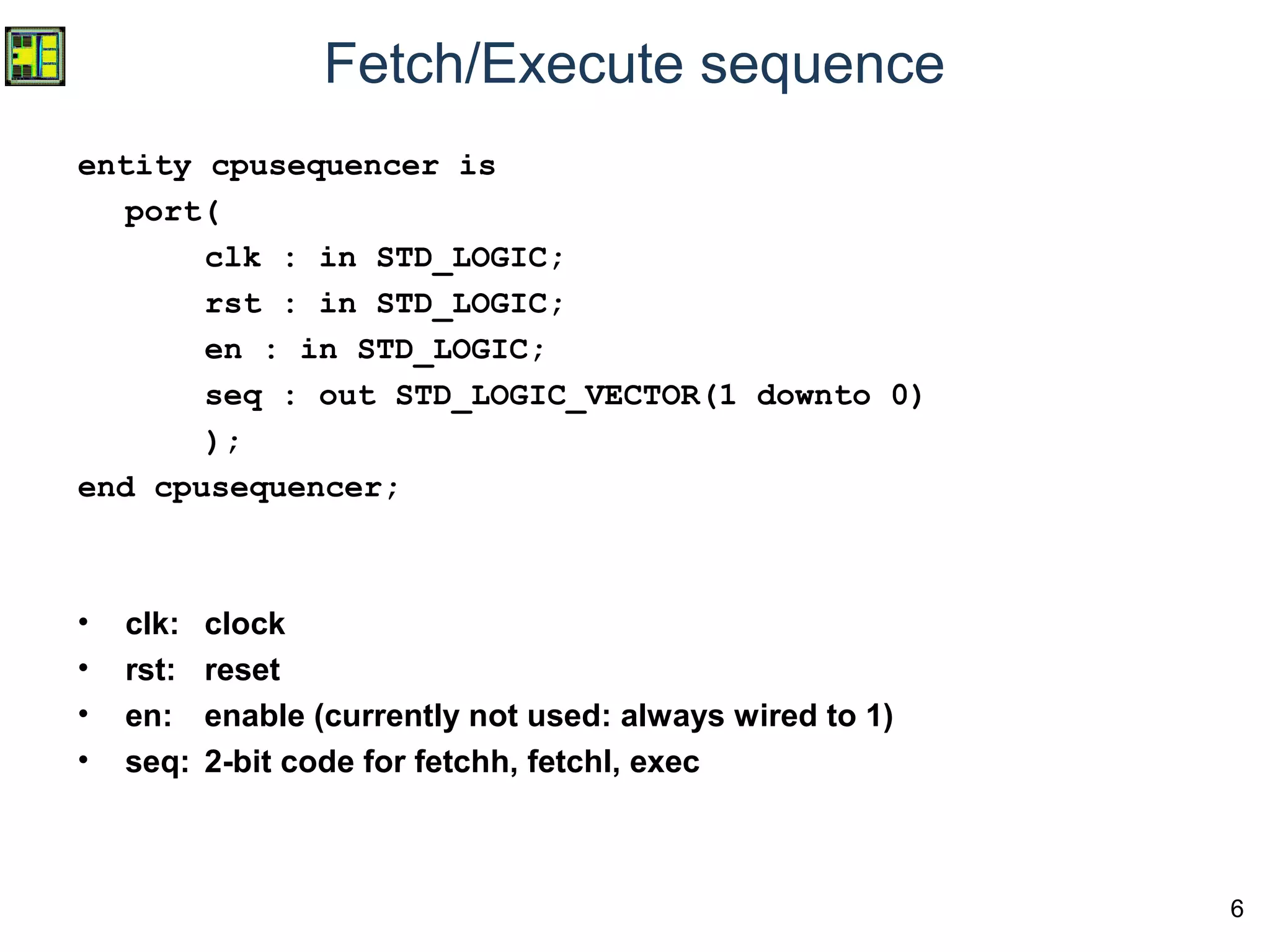
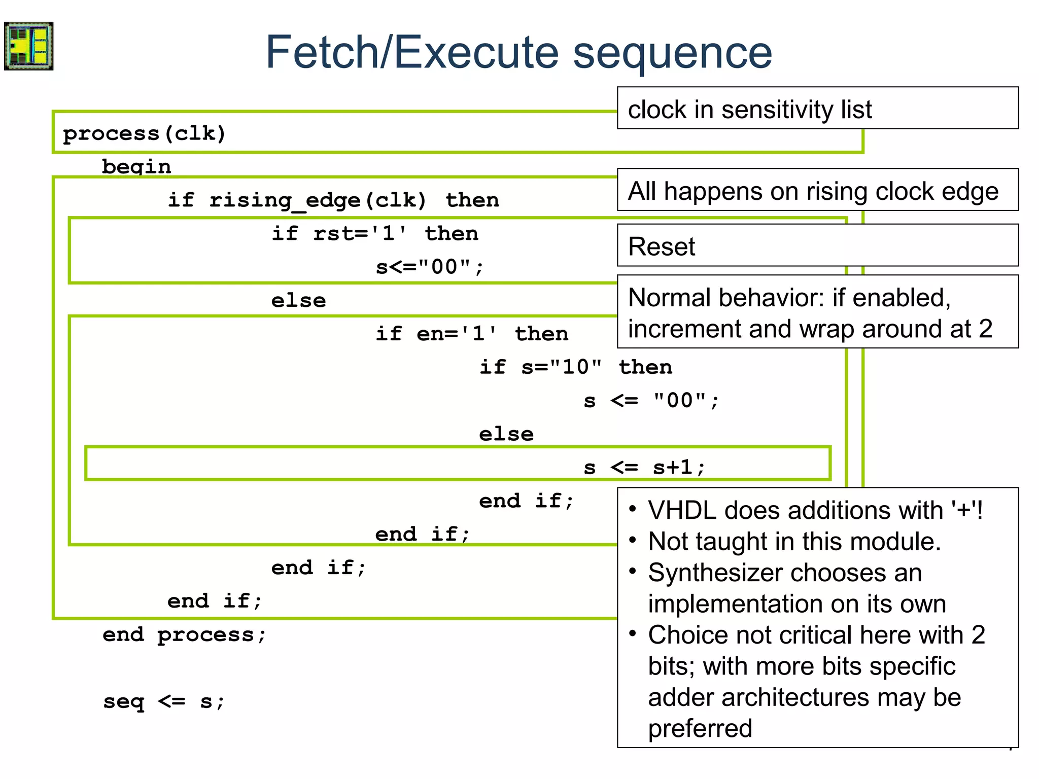
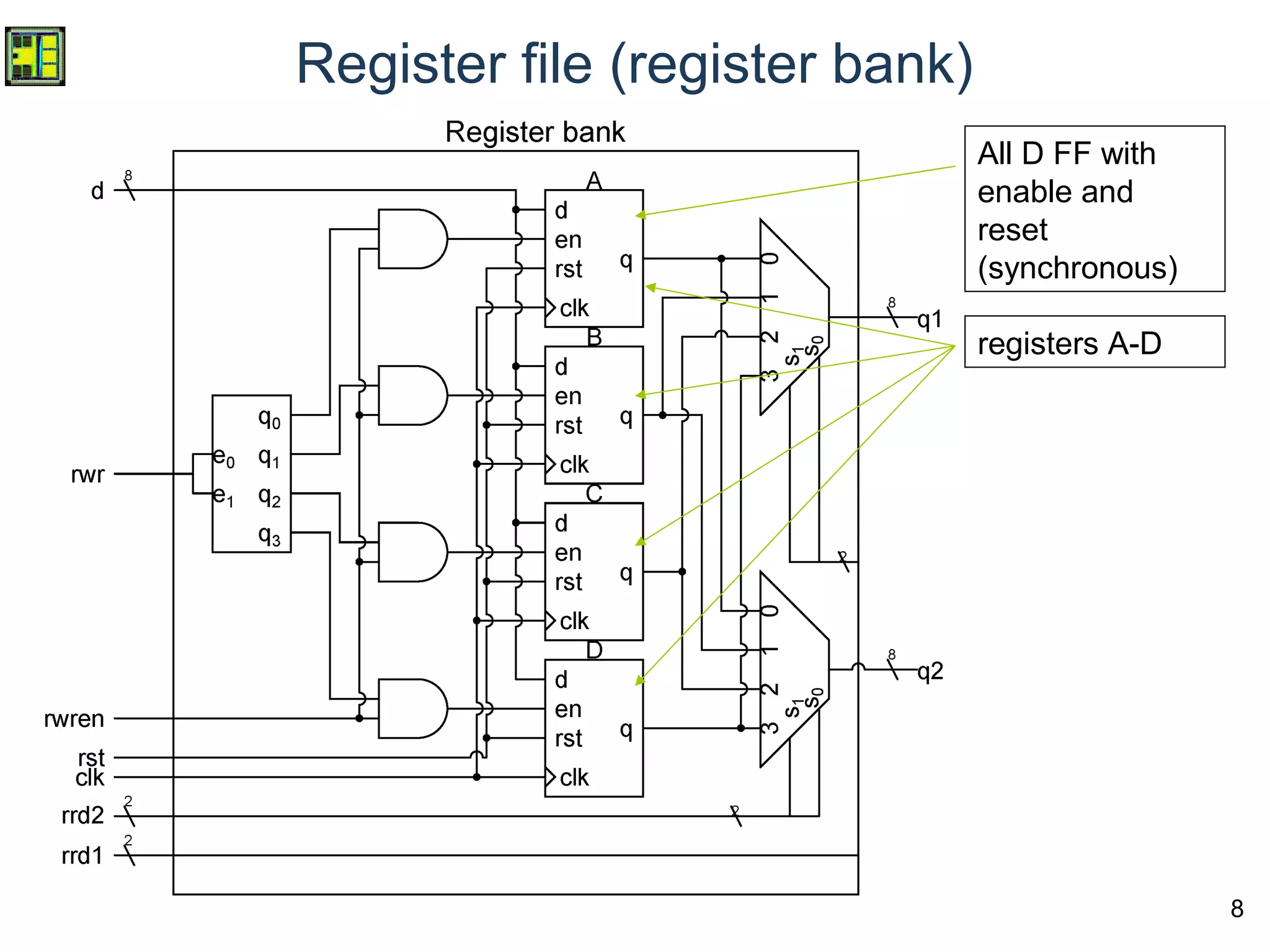
![9
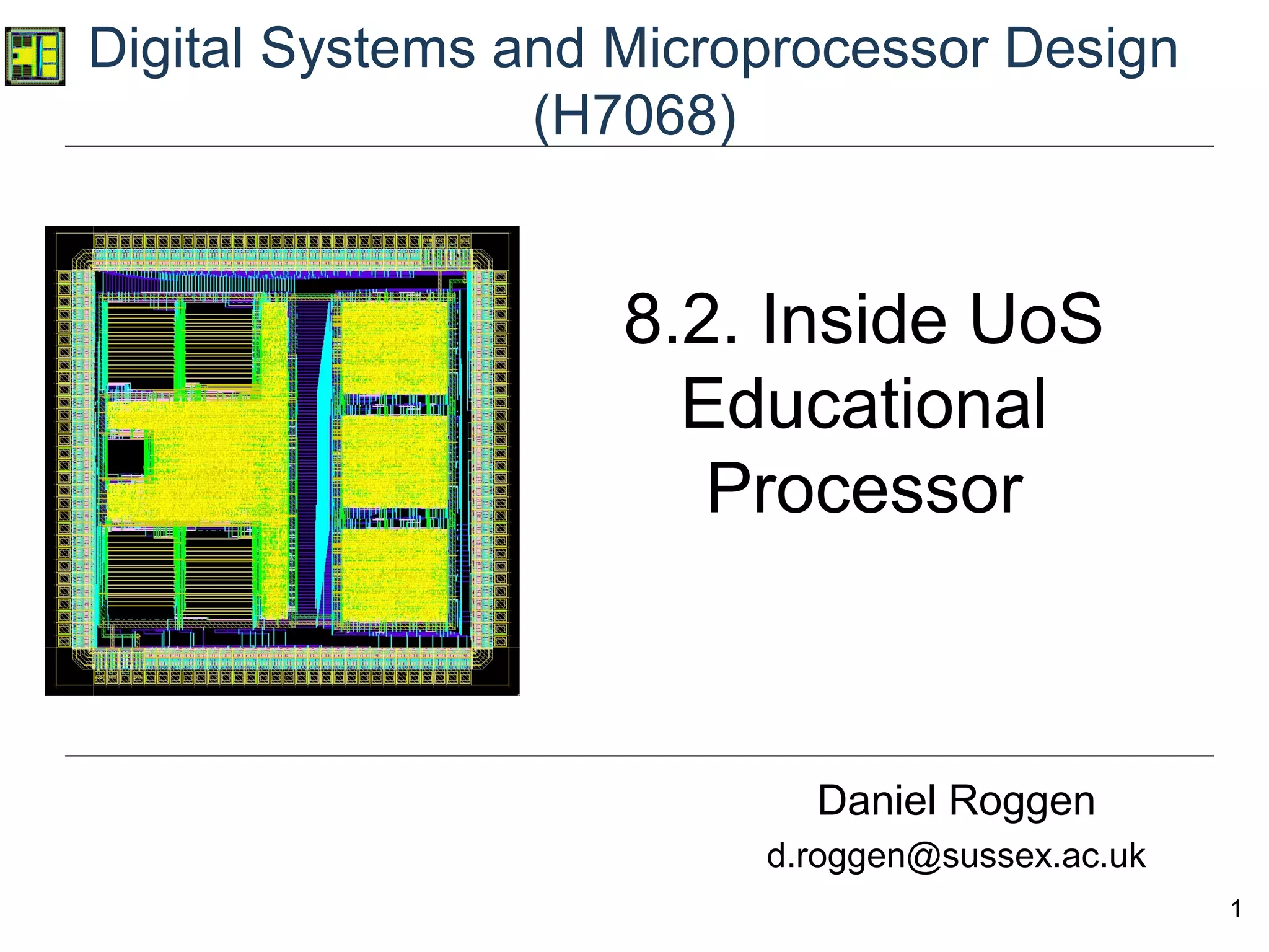
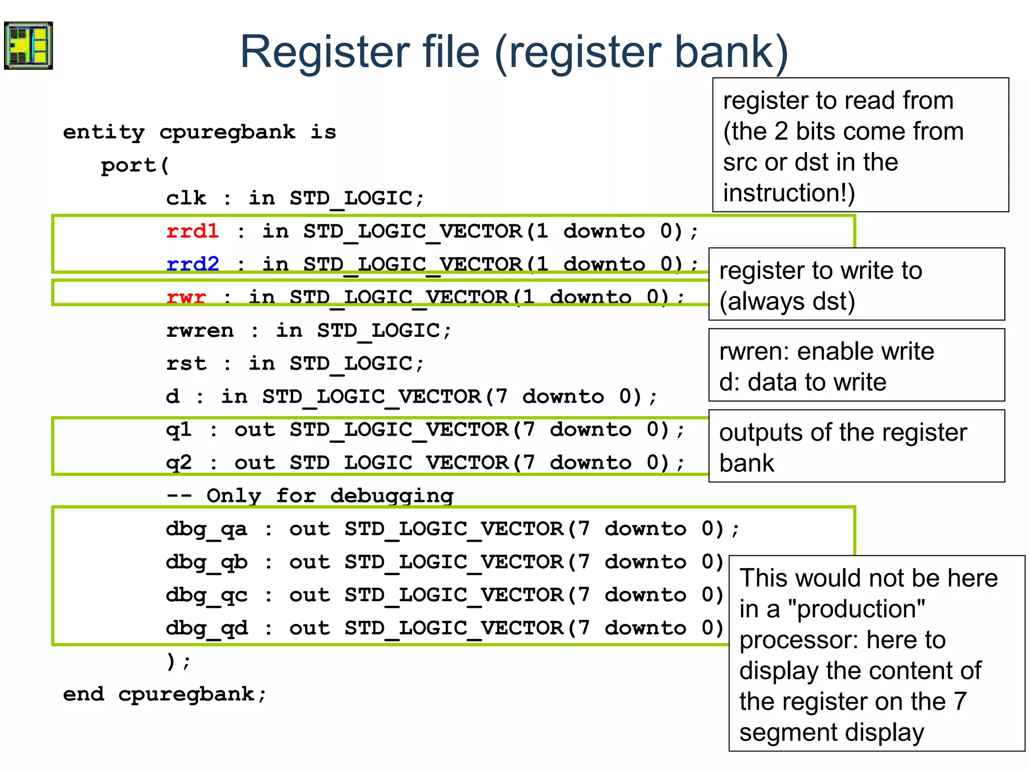
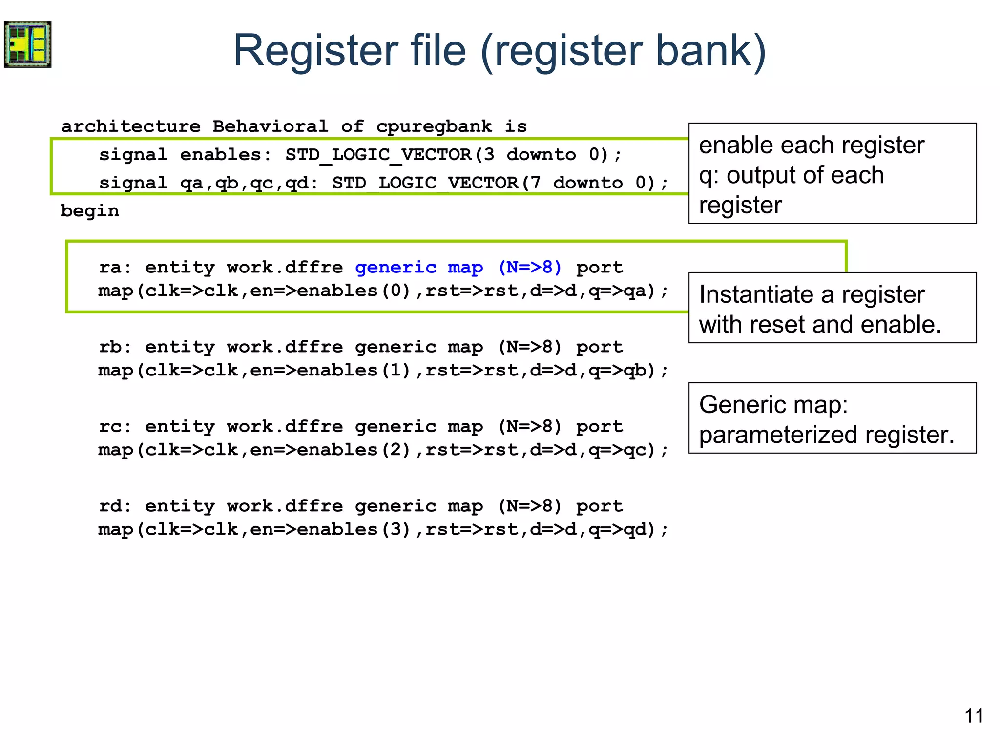
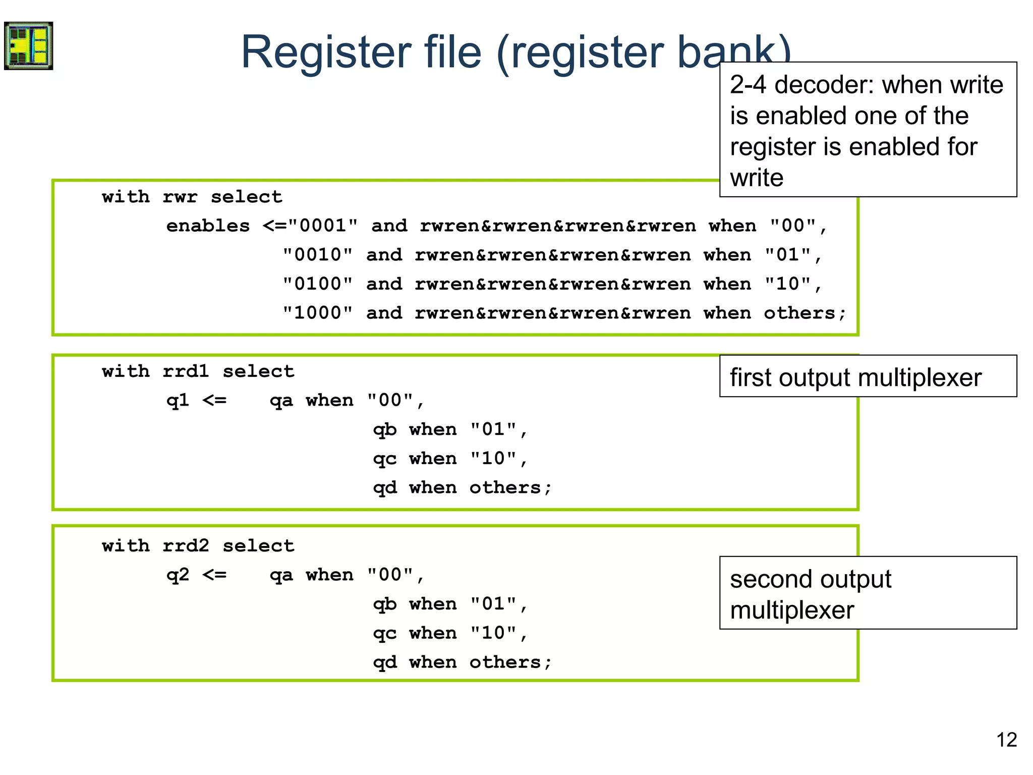
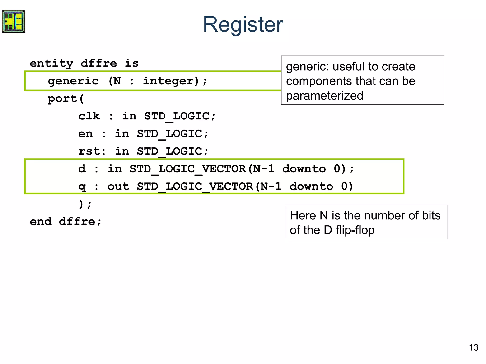
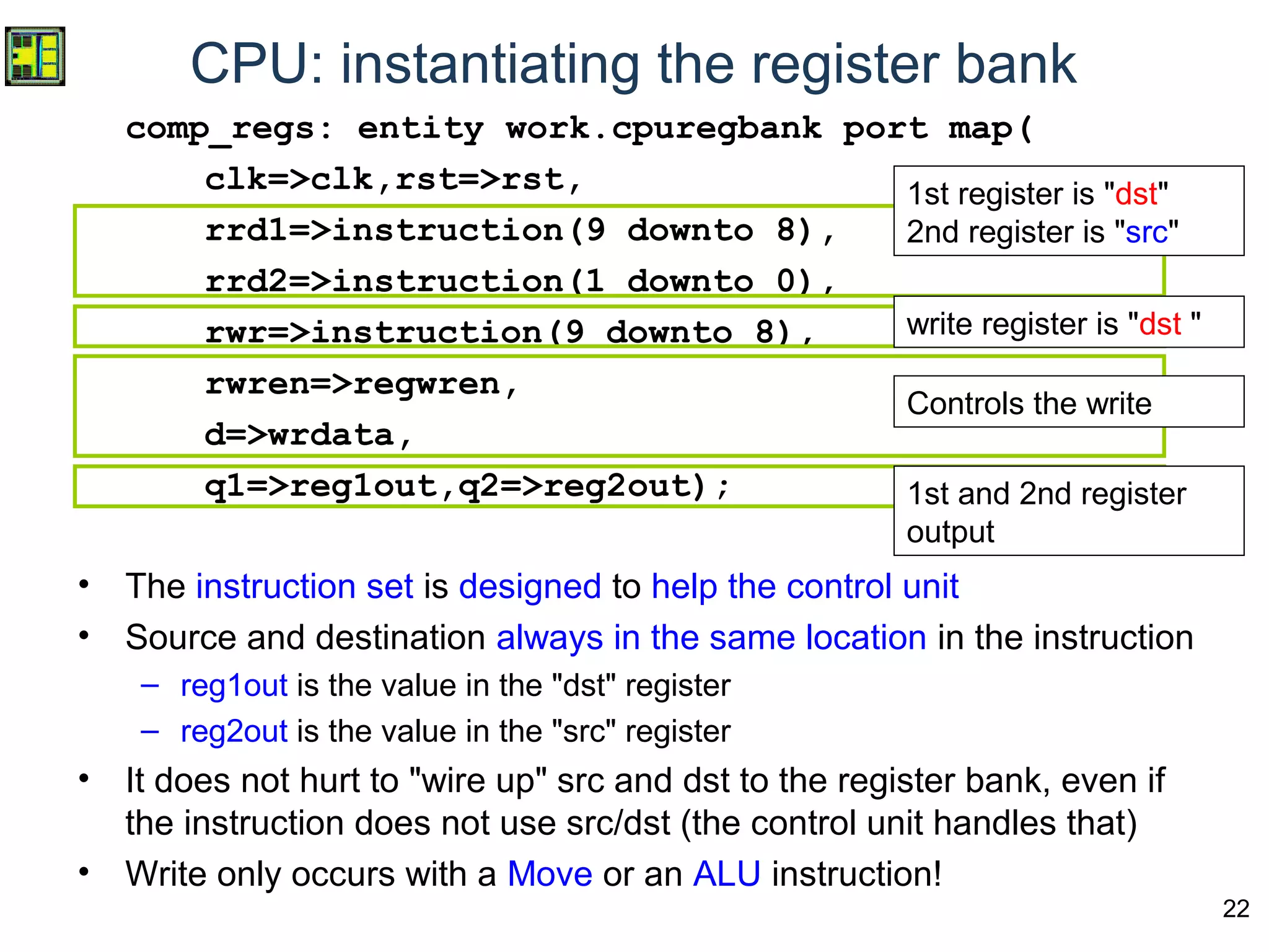
Register file (register bank)
• Reminder: move instruction
• Always operation between dst and src, with result in dst
• Let's consider what to read from our register bank:
– The register defined by dst and src (even if we deal with an
immediate-this is handled elsewhere
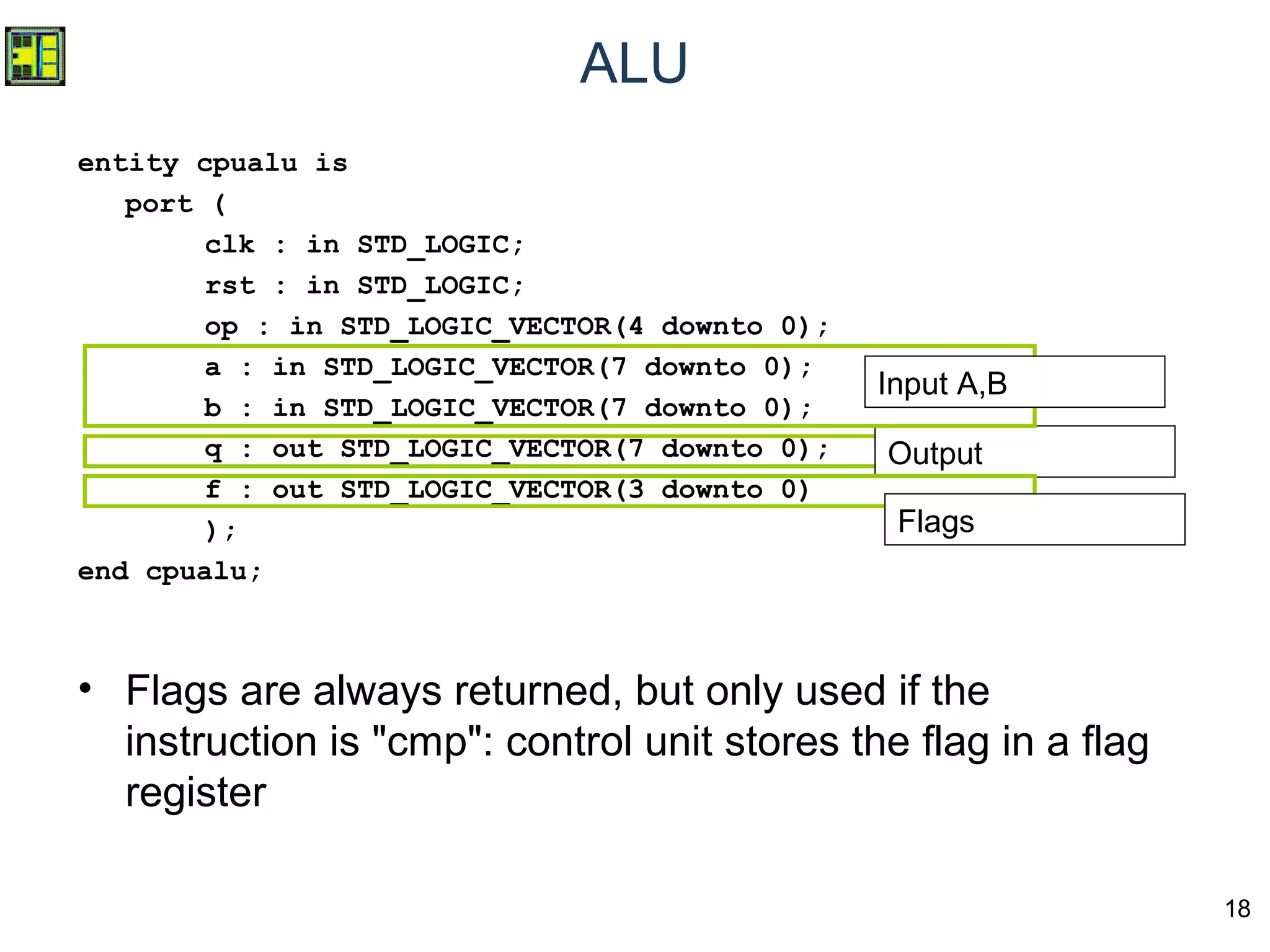
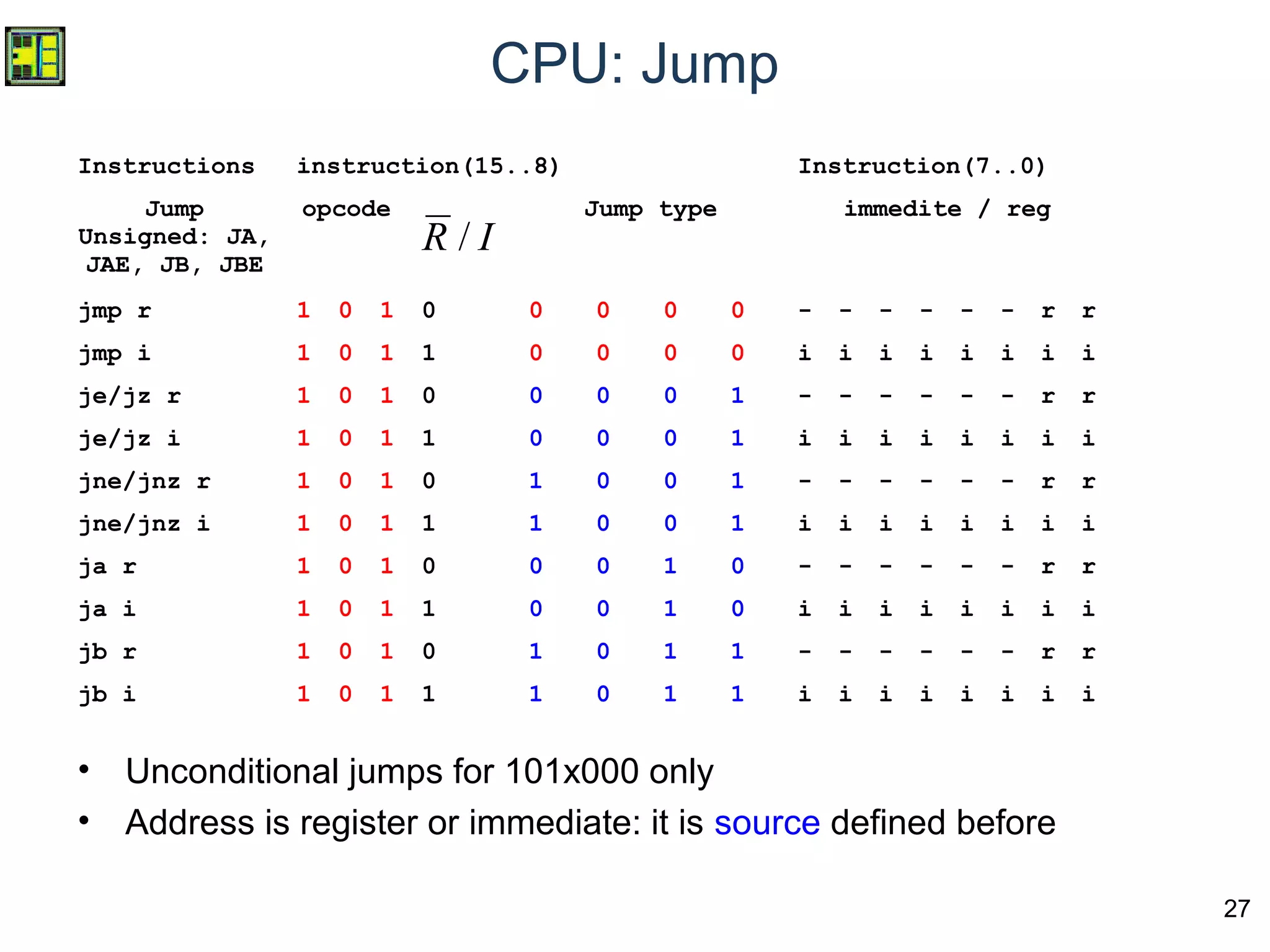
Instructions instruction(15..8) Instruction(7..0)
Move Opcode dd#m sd#m dreg src
mov r, r 0 0 0 0 0 0 r r - - - - - - r r
mov r, i 0 0 0 1 0 0 r r i i i i i i i i
mov r, [r] 0 0 0 0 0 1 r r - - - - - - r r
mov r, [i] 0 0 0 1 0 1 r r i i i i i i i i
mov [r], r 0 0 0 0 1 0 r r - - - - - - r r
mov [r], i 0 0 0 1 1 0 r r i i i i i i i i](https://image.slidesharecdn.com/w82insideuoseducationalprocessor-171205211049/75/W8_2-Inside-the-UoS-Educational-Processor-9-2048.jpg)
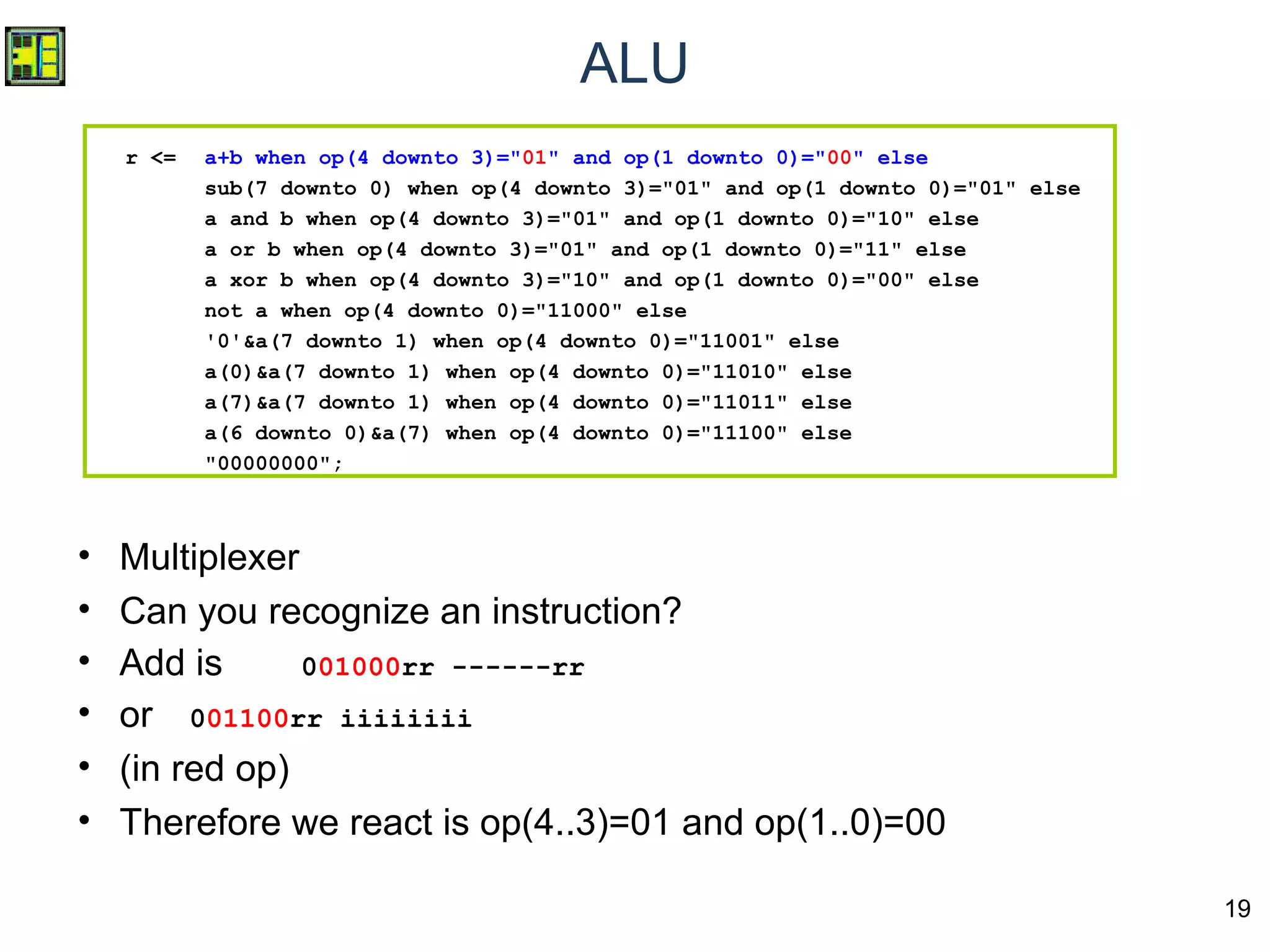
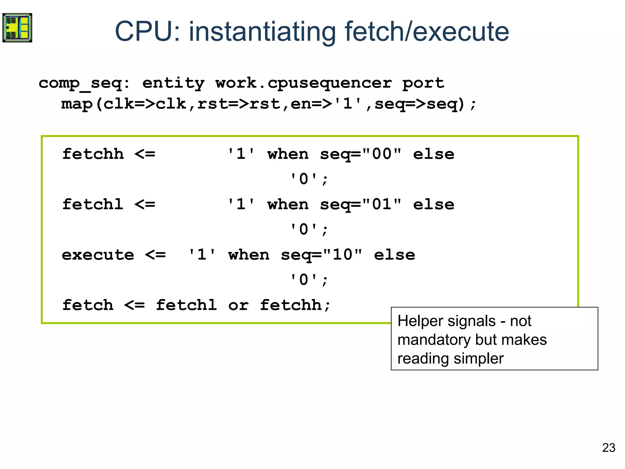
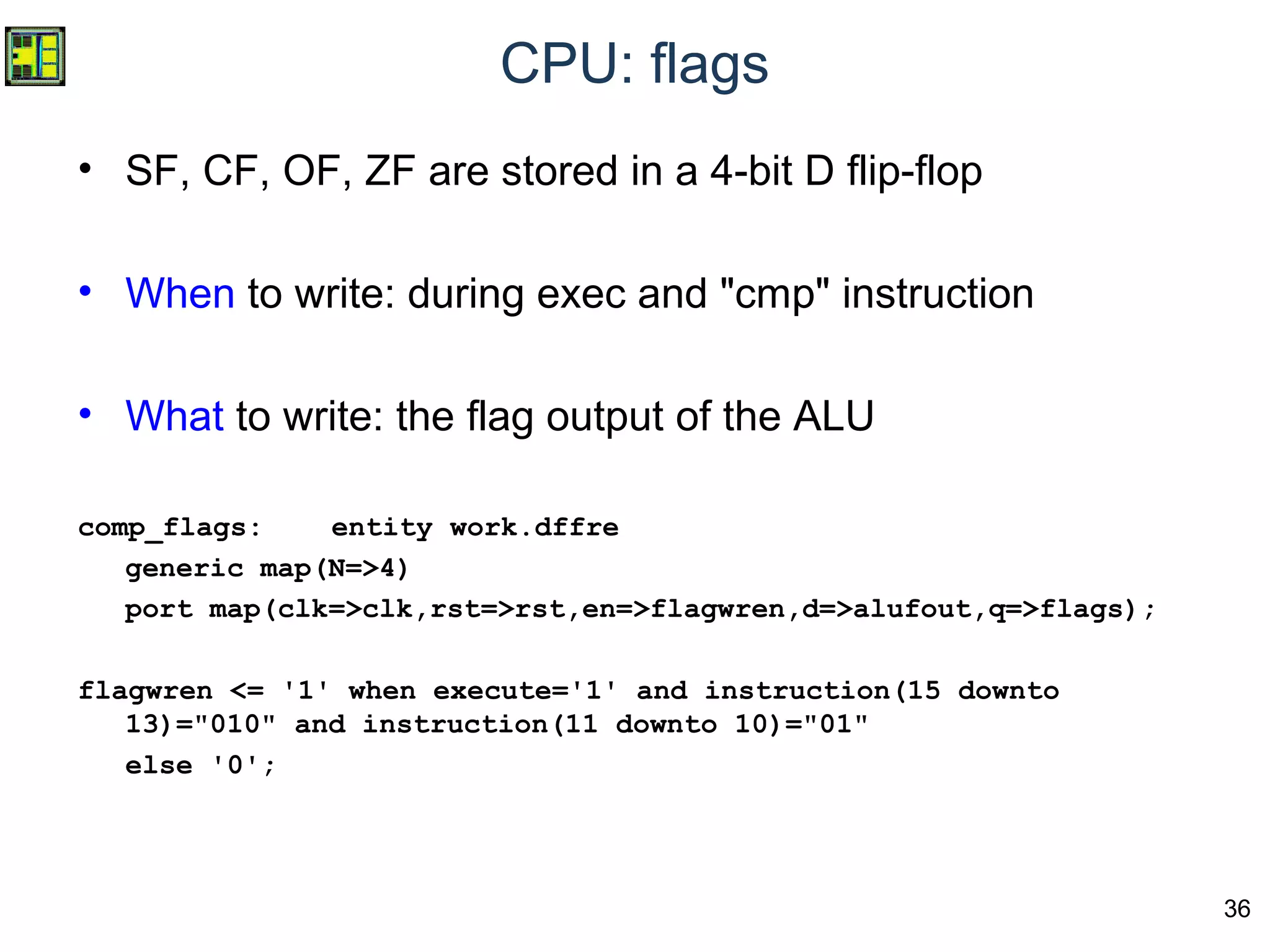
![34
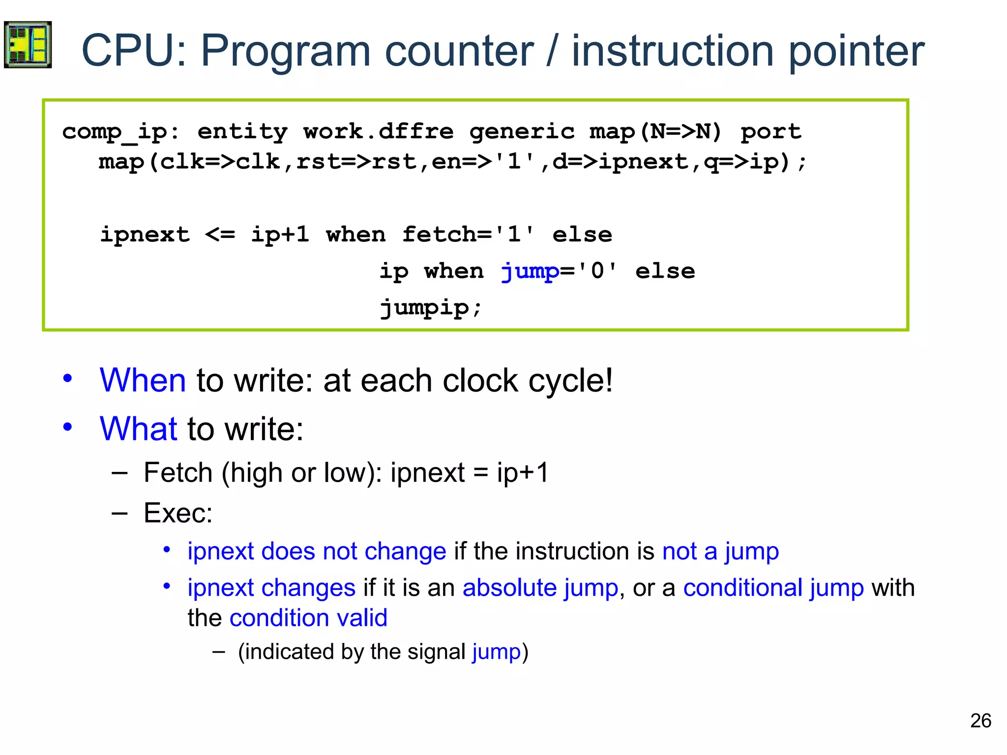
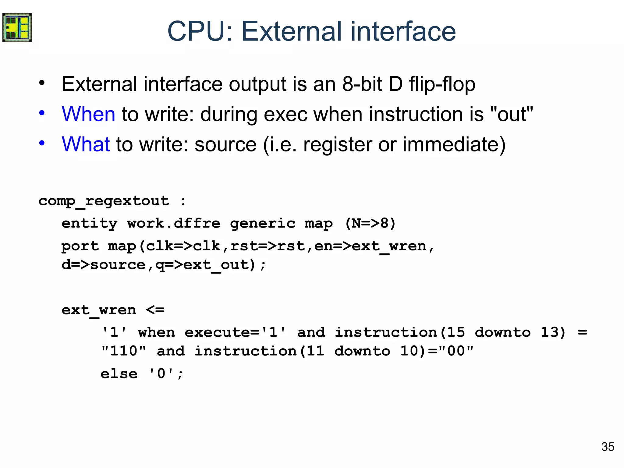
CPU: when to write to memory?
• Move to memory during the exec cycle:
– mov [b],23h
ram_we <=
'1' when execute='1' and instruction(15 downto 13)="000"
and instruction(11 downto 10)="10"
else '0';](https://image.slidesharecdn.com/w82insideuoseducationalprocessor-171205211049/75/W8_2-Inside-the-UoS-Educational-Processor-34-2048.jpg)
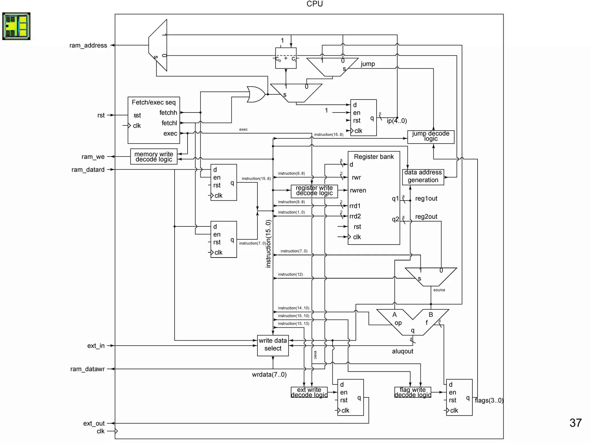
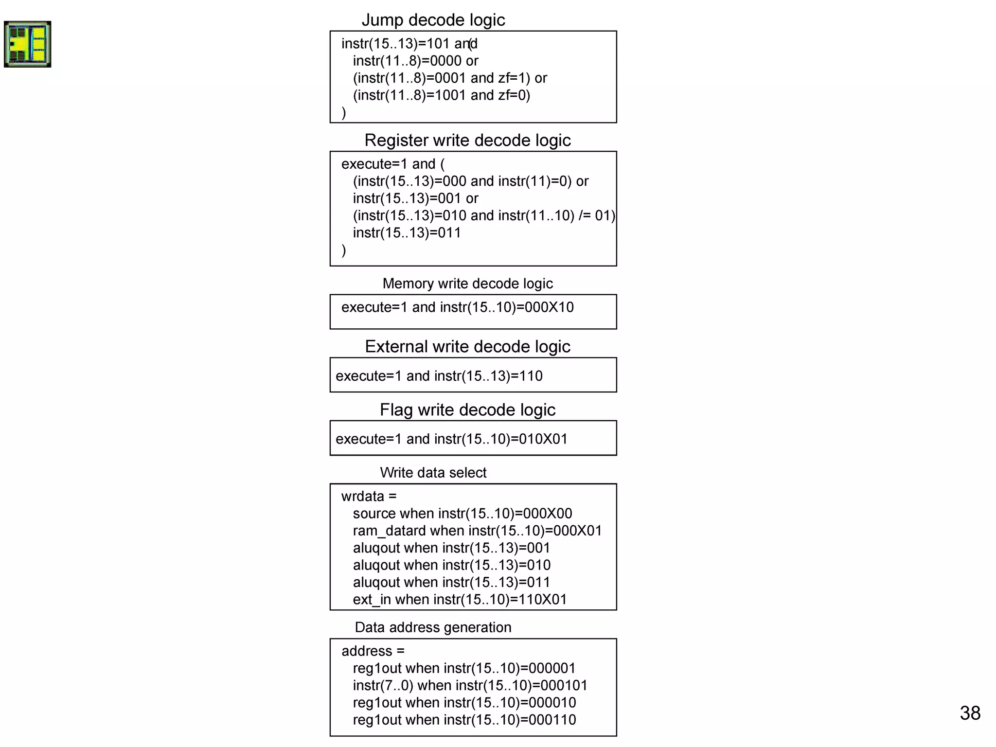

The document outlines the design of a digital system and microprocessor architecture, detailing various components such as the educational processor, fetch/execute sequence, register bank, and arithmetic logic unit (ALU). It includes VHDL specifications for fundamental operations and describes how instructions are processed, including reading from registers and executing arithmetic operations. Additionally, it covers the implementation of control logic for instruction fetching, processing, and managing jumps within the instruction set.


![[2012 CodeEngn Conference 06] pwn3r - Secuinside 2012 CTF 예선 문제풀이](https://cdn.slidesharecdn.com/ss_thumbnails/20126thcodeengnpwn3rsecuinside2012ctf-130525233500-phpapp02-thumbnail.jpg?width=640&height=640&fit=bounds)