Download to read offline

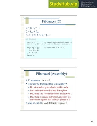
![7
Verilog Code
// top level design includes both mips processor and memory
module mips_mem #(parameter WIDTH = 8, REGBITS = 3)(clk, reset);
input clk, reset;
wire memread, memwrite;
wire [WIDTH-1:0] adr, writedata;
wire [WIDTH-1:0] memdata;
// instantiate the mips processor
mips #(WIDTH,REGBITS) mips(clk, reset, memdata, memread,
memwrite, adr, writedata);
// instantiate memory for code and data
exmem #(WIDTH) exmem(clk, memwrite, adr, writedata, memdata);
endmodule
Block Diagram](https://image.slidesharecdn.com/anexamplemips-230805204410-5edcdf4d/85/An-Example-MIPS-7-320.jpg)
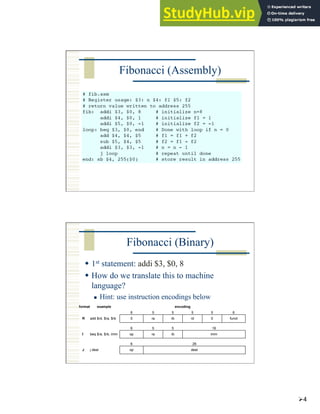
![8
// simplified MIPS processor
module mips #(parameter WIDTH = 8, REGBITS = 3)
(input clk, reset,
input [WIDTH-1:0] memdata,
output memread, memwrite,
output [WIDTH-1:0] adr, writedata);
wire [31:0] instr;
wire zero, alusrca, memtoreg, iord, pcen, regwrite, regdst;
wire [1:0] aluop,pcsource,alusrcb;
wire [3:0] irwrite;
wire [2:0] alucont;
controller cont(clk, reset, instr[31:26], zero, memread, memwrite,
alusrca, memtoreg, iord, pcen, regwrite, regdst,
pcsource, alusrcb, aluop, irwrite);
alucontrol ac(aluop, instr[5:0], alucont);
datapath #(WIDTH, REGBITS)
dp(clk, reset, memdata, alusrca, memtoreg, iord, pcen,
regwrite, regdst, pcsource, alusrcb, irwrite, alucont,
zero, instr, adr, writedata);
endmodule
Top-level
code
Controller
Parameters
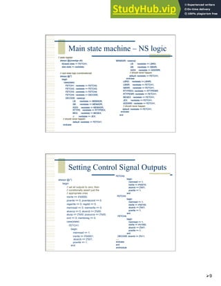
module controller(input clk, reset,
input [5:0] op,
input zero,
output reg memread, memwrite, alusrca, memtoreg, iord,
output pcen,
output reg regwrite, regdst,
output reg [1:0] pcsource, alusrcb, aluop,
output reg [3:0] irwrite);
parameter FETCH1 = 4'b0001;
parameter FETCH2 = 4'b0010;
parameter FETCH3 = 4'b0011;
parameter FETCH4 = 4'b0100;
parameter DECODE = 4'b0101;
parameter MEMADR = 4'b0110;
parameter LBRD = 4'b0111;
parameter LBWR = 4'b1000;
parameter SBWR = 4'b1001;
parameter RTYPEEX = 4'b1010;
parameter RTYPEWR = 4'b1011;
parameter BEQEX = 4'b1100;
parameter JEX = 4'b1101;
parameter ADDIWR = 4'b1110; // added for ADDI
parameter LB = 6'b100000;
parameter SB = 6'b101000;
parameter RTYPE = 6'b0;
parameter BEQ = 6'b000100;
parameter J = 6'b000010;
parameter ADDI = 6'b001000; /// added for ADDI
reg [3:0] state, nextstate;
reg pcwrite, pcwritecond;
State Encodings...
Opcodes...
Local reg variables...](https://image.slidesharecdn.com/anexamplemips-230805204410-5edcdf4d/85/An-Example-MIPS-8-320.jpg)
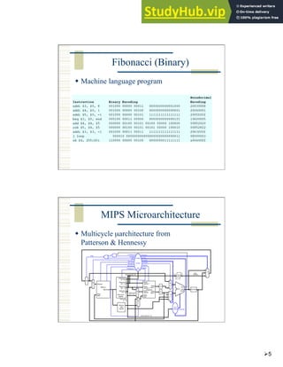
![10
Verilog: alucontrol
module alucontrol(input [1:0] aluop,
input [5:0] funct,
output reg [2:0] alucont);
always @(*)
case(aluop)
2'b00: alucont <= 3'b010; // add for lb/sb/addi
2'b01: alucont <= 3'b110; // sub (for beq)
default: case(funct) // R-Type instructions
6'b100000: alucont <= 3'b010; // add (for add)
6'b100010: alucont <= 3'b110; // subtract (for sub)
6'b100100: alucont <= 3'b000; // logical and (for and)
6'b100101: alucont <= 3'b001; // logical or (for or)
6'b101010: alucont <= 3'b111; // set on less (for slt)
default: alucont <= 3'b101; // should never happen
endcase
endcase
endmodule
Verilog: alu
module alu #(parameter WIDTH = 8)
(input [WIDTH-1:0] a, b,
input [2:0] alucont,
output reg [WIDTH-1:0] result);
wire [WIDTH-1:0] b2, sum, slt;
assign b2 = alucont[2] ? ˜b:b;
assign sum = a + b2 + alucont[2];
// slt should be 1 if most significant bit of sum is 1
assign slt = sum[WIDTH-1];
always@(*)
case(alucont[1:0])
2'b00: result <= a & b;
2'b01: result <= a ¦ b;
2'b10: result <= sum;
2'b11: result <= slt;
endcase
endmodule](https://image.slidesharecdn.com/anexamplemips-230805204410-5edcdf4d/85/An-Example-MIPS-10-320.jpg)
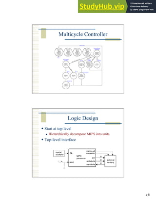
![11
Verilog: regfile
module regfile #(parameter WIDTH = 8, REGBITS = 3)
(input clk,
input regwrite,
input [REGBITS-1:0] ra1, ra2, wa,
input [WIDTH-1:0] wd,
output [WIDTH-1:0] rd1, rd2);
reg [WIDTH-1:0] RAM [(1<<REGBITS)-1:0];
// three ported register file
// read two ports (combinational)
// write third port on rising edge of clock
// register 0 is hardwired to 0
always @(posedge clk)
if (regwrite) RAM[wa] <= wd;
assign rd1 = ra1 ? RAM[ra1] : 0;
assign rd2 = ra2 ? RAM[ra2] : 0;
endmodule
Verlog: Other
stuff
module zerodetect #(parameter WIDTH = 8)
(input [WIDTH-1:0] a,
output y);
assign y = (a==0);
endmodule
module flop #(parameter WIDTH = 8)
(input clk,
input [WIDTH-1:0] d,
output reg [WIDTH-1:0] q);
always @(posedge clk)
q <= d;
endmodule
module flopen #(parameter WIDTH = 8)
(input clk, en,
input [WIDTH-1:0] d,
output reg [WIDTH-1:0] q);
always @(posedge clk)
if (en) q <= d;
endmodule
module flopenr #(parameter WIDTH = 8)
(input clk, reset, en,
input [WIDTH-1:0] d,
output reg [WIDTH-1:0] q);
always @(posedge clk)
if (reset) q <= 0;
else if (en) q <= d;
endmodule
module mux2 #(parameter WIDTH = 8)
(input [WIDTH-1:0] d0, d1,
input s,
output [WIDTH-1:0] y);
assign y = s ? d1 : d0;
endmodule
module mux4 #(parameter WIDTH = 8)
(input [WIDTH-1:0] d0, d1, d2, d3,
input [1:0] s,
output reg [WIDTH-1:0] y);
always @(*)
case(s)
2'b00: y <= d0;
2'b01: y <= d1;
2'b10: y <= d2;
2'b11: y <= d3;
endcase
endmodule](https://image.slidesharecdn.com/anexamplemips-230805204410-5edcdf4d/85/An-Example-MIPS-11-320.jpg)
![12
MIPS Microarchitecture
Multicycle µarchitecture from
Patterson & Hennessy
module datapath #(parameter WIDTH = 8, REGBITS = 3)
(input clk, reset,
input [WIDTH-1:0] memdata,
input alusrca, memtoreg, iord, pcen, regwrite, regdst,
input [1:0] pcsource, alusrcb,
input [3:0] irwrite,
input [2:0] alucont,
output zero,
output [31:0] instr,
output [WIDTH-1:0] adr, writedata);
// the size of the parameters must be changed to match the WIDTH parameter
localparam CONST̲ZERO = 8'b0;
localparam CONST̲ONE = 8'b1;
wire [REGBITS-1:0] ra1, ra2, wa;
wire [WIDTH-1:0] pc, nextpc, md, rd1, rd2, wd, a, src1, src2, aluresult,
aluout, constx4;
// shift left constant field by 2
assign constx4 = {instr[WIDTH-3:0],2'b00};
// register file address fields
assign ra1 = instr[REGBITS+20:21];
assign ra2 = instr[REGBITS+15:16];
mux2 #(REGBITS) regmux(instr[REGBITS+15:16], instr[REGBITS+10:11], regdst, wa);
Verilog:
Datapath 1](https://image.slidesharecdn.com/anexamplemips-230805204410-5edcdf4d/85/An-Example-MIPS-12-320.jpg)
![13
// independent of bit width, load instruction into four 8-bit registers over four cycles
flopen #(8) ir0(clk, irwrite[0], memdata[7:0], instr[7:0]);
flopen #(8) ir1(clk, irwrite[1], memdata[7:0], instr[15:8]);
flopen #(8) ir2(clk, irwrite[2], memdata[7:0], instr[23:16]);
flopen #(8) ir3(clk, irwrite[3], memdata[7:0], instr[31:24]);
// datapath
flopenr #(WIDTH) pcreg(clk, reset, pcen, nextpc, pc);
flop #(WIDTH) mdr(clk, memdata, md);
flop #(WIDTH) areg(clk, rd1, a);
flop #(WIDTH) wrd(clk, rd2, writedata);
flop #(WIDTH) res(clk, aluresult, aluout);
mux2 #(WIDTH) adrmux(pc, aluout, iord, adr);
mux2 #(WIDTH) src1mux(pc, a, alusrca, src1);
mux4 #(WIDTH) src2mux(writedata, CONST̲ONE, instr[WIDTH-1:0],
constx4, alusrcb, src2);
mux4 #(WIDTH) pcmux(aluresult, aluout, constx4, CONST̲ZERO, pcsource, nextpc);
mux2 #(WIDTH) wdmux(aluout, md, memtoreg, wd);
regfile #(WIDTH,REGBITS) rf(clk, regwrite, ra1, ra2, wa, wd, rd1, rd2);
alu #(WIDTH) alunit(src1, src2, alucont, aluresult);
zerodetect #(WIDTH) zd(aluresult, zero);
endmodule
Verilog:
Datapath 2
Logic Design
Start at top level
Hierarchically decompose MIPS into units
Top-level interface](https://image.slidesharecdn.com/anexamplemips-230805204410-5edcdf4d/85/An-Example-MIPS-13-320.jpg)
![14
Verilog: exmemory
// external memory accessed by MIPS
module exmemory #(parameter WIDTH = 8)
(clk, memwrite, adr, writedata, memdata);
input clk;
input memwrite;
input [WIDTH-1:0] adr, writedata;
output reg [WIDTH-1:0] memdata;
reg [31:0] RAM [(1<<WIDTH-2)-1:0];
wire [31:0] word;
initial
begin
$readmemh("memfile.dat",RAM);
end
// read and write bytes from 32-bit word
always @(posedge clk)
if(memwrite)
case (adr[1:0])
2'b00: RAM[adr>>2][7:0] <= writedata;
2'b01: RAM[adr>>2][15:8] <= writedata;
2'b10: RAM[adr>>2][23:16] <= writedata;
2'b11: RAM[adr>>2][31:24] <= writedata;
endcase
assign word = RAM[adr>>2];
always @(*)
case (adr[1:0])
2'b00: memdata <= word[7:0];
2'b01: memdata <= word[15:8];
2'b10: memdata <= word[23:16];
2'b11: memdata <= word[31:24];
endcase
endmodule
Synthesized memory?
If you synthesize the Verilog, you’ll get a
memory
But – it will be huge!
It will be made of your DFF cells
plus synthesized address decoders
Custom memory is much smaller
but much trickier to get right
… see details in VGA slides …](https://image.slidesharecdn.com/anexamplemips-230805204410-5edcdf4d/85/An-Example-MIPS-14-320.jpg)
![15
Verilog: exmemory
// external memory accessed by MIPS
module exmem #(parameter WIDTH = 8)
(clk, memwrite, adr, writedata,
memdata);
input clk;
input memwrite;
input [WIDTH-1:0] adr, writedata;
output [WIDTH-1:0] memdata;
wire memwriteB, clkB;
// UMC RAM has active low write enable...
not(memwriteB, memwrite);
// Looks like you need to clock the memory early
// to make it work with the current control...
not(clkB, clk);
// Instantiate the UMC SPRAM module
UMC130SPRAM̲8̲8 mips̲ram (
.CK(clkB),
.CEN(1'b0),
.WEN(memwriteB),
.OEN(1'b0),
.ADR(adr),
.DI(writedata),
.DOUT(memdata));
endmodule
MIPS (8-bit) size comparison
One big EDI run of the whole thing
With some work, could probably get this in a single TCU...](https://image.slidesharecdn.com/anexamplemips-230805204410-5edcdf4d/85/An-Example-MIPS-15-320.jpg)


This document describes the design and implementation of a MIPS processor using Verilog. It begins with an overview of the MIPS architecture and instruction set. It then provides Verilog code for the top-level processor module, controller, datapath, register file, ALU, and other components. Diagrams of the processor microarchitecture and multicycle controller state machine are also shown. The document focuses on hierarchically designing the MIPS processor using a structural Verilog approach and parameterized modules.