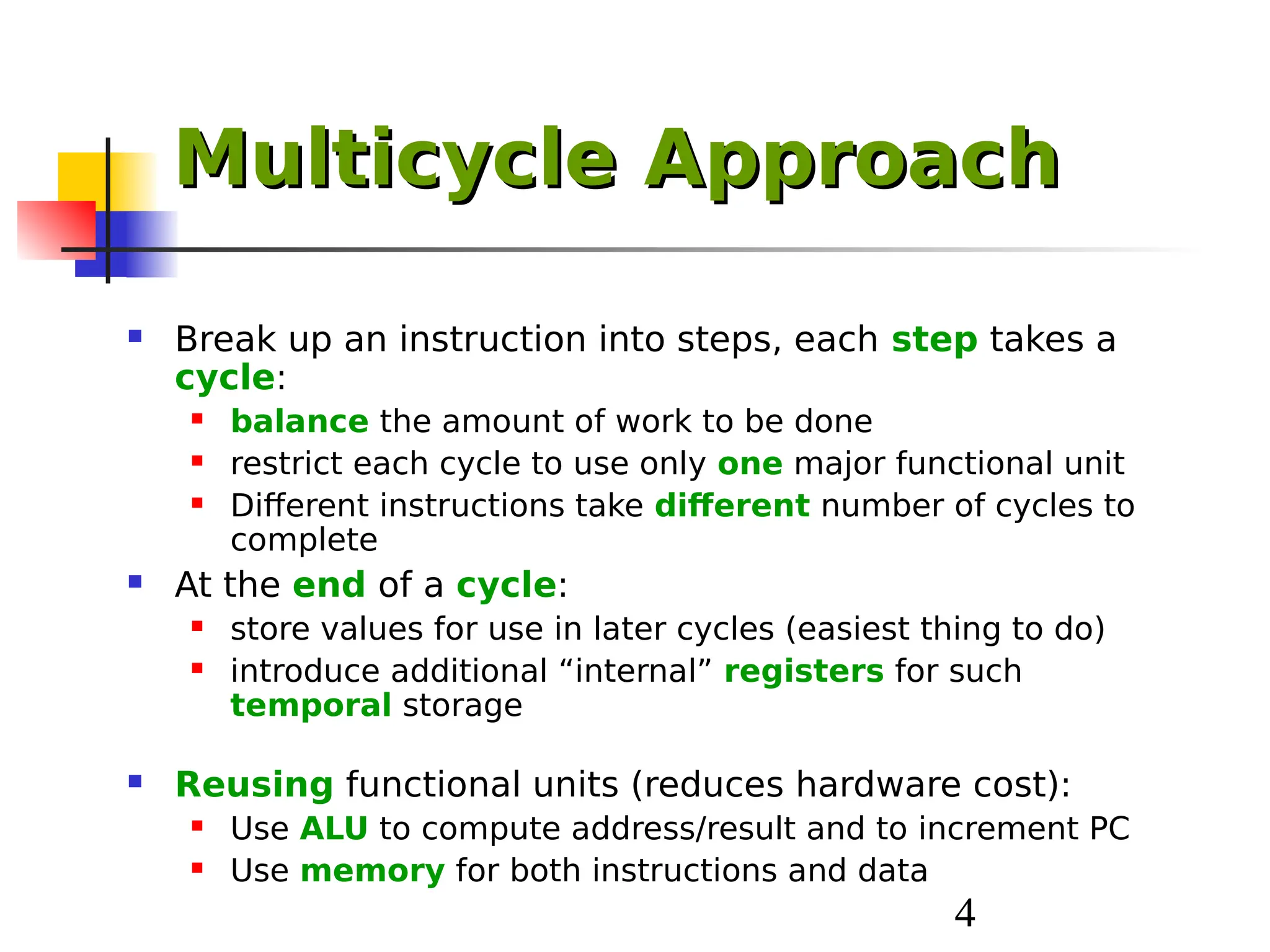
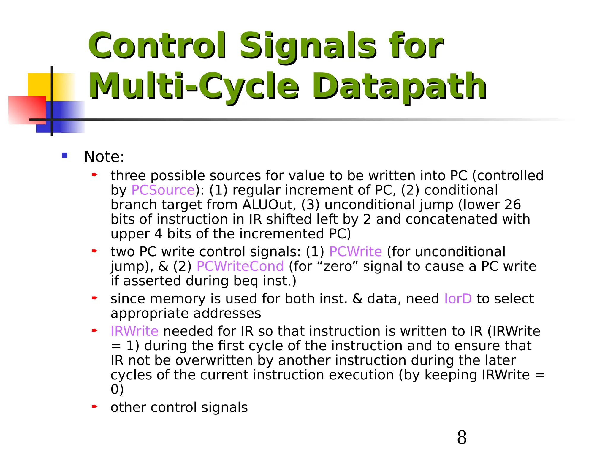
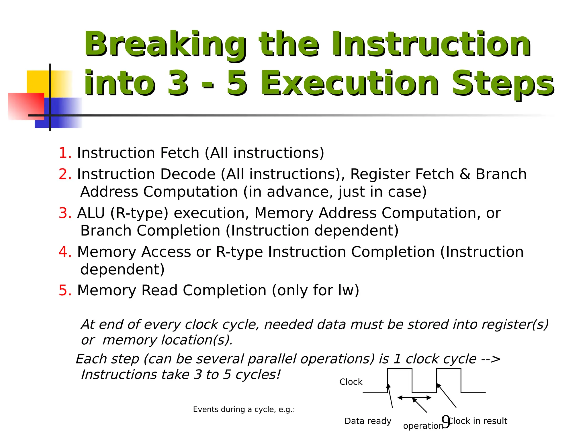
SlideShare a Scribd company logo
1 of 16
Download to read offline
1
(Based on text: David A. Patterson & John L. Hennessy, Computer Organization and Design:
The Hardware/Software Interface, 3rd
Ed., Morgan Kaufmann, 2007)
Processor: Multi-
Processor: Multi-
Cycle Datapath &
Cycle Datapath &
Control
Control
2
COURSE CONTENTS
COURSE CONTENTS
 Introduction
 Instructions
 Computer Arithmetic
 Performance
 Processor: Datapath
Processor: Datapath
 Processor: Control
Processor: Control
 Pipelining Techniques
 Memory
 Input/Output Devices
3
PROCESSOR:
PROCESSOR:
DATAPATH & CONTROL
DATAPATH & CONTROL
 Multi-Cycle Datapath
 Multi-Cycle Control
 Additional Registers and
Multiplexers
4
 Break up an instruction into steps, each step takes a
cycle:
 balance the amount of work to be done
 restrict each cycle to use only one major functional unit
 Different instructions take different number of cycles to
complete
 At the end of a cycle:
 store values for use in later cycles (easiest thing to do)
 introduce additional “internal” registers for such
temporal storage
 Reusing functional units (reduces hardware cost):
 Use ALU to compute address/result and to increment PC
 Use memory for both instructions and data
Multicycle Approach
Multicycle Approach
5
 Additional “internal registers”:
 Instruction register (IR) -- to hold current instruction
 Memory data register (MDR) -- to hold data read from memory
 A register (A) & B register (B) -- to hold register operand values from register files
 ALUOut register (ALUOut) -- to hold output of ALU, also serves as memory address
register (MAR)
 All registers except IR hold data only between a pair of adjacent cycles and thus do
not need write control signals; IR holds instructions till end of instruction, hence
needs a write control signal
Multi-Cycle Datapath:
Additional Registers
Shift
left 2
PC
Memory
Data
Write
data
M
u
x
0
1
Registers
Write
register
Write
data
Read
data 1
Read
data 2
Read
register 1
Read
register 2
M
u
x
0
1
M
u
x
0
1
4
Instruction
[15– 0]
Sign
extend
32
16
Instruction
[25– 21]
Instruction
[20– 16]
Instruction
[15– 0]
Instruction
register
1 M
u
x
0
3
2
M
u
x
ALU
result
ALU
Zero
Memory
data
register
Instruction
[15– 11]
A
B
ALUOut
0
1
Address
Inst /
Note: we ignore jump inst here
6
 Additional multiplexors:
 Mux for first ALU input -- to select A or PC (since we use ALU for both
address/result computation & PC increment)
 Bigger mux for second ALU input -- due to two additional inputs: 4 (for normal PC
increment) and the sign-extended & shifted offset field (in branch address
computation)
 Mux for memory address input -- to select instruction address or data address
Multicycle Datapath:
Additional Multiplexors
Shift
left 2
PC
Memory
Data
Write
data
M
u
x
0
1
Registers
Write
register
Write
data
Read
data 1
Read
data 2
Read
register 1
Read
register 2
M
u
x
0
1
M
u
x
0
1
4
Instruction
[15– 0]
Sign
extend
32
16
Instruction
[25– 21]
Instruction
[20– 16]
Instruction
[15– 0]
Instruction
register
1 M
u
x
0
3
2
M
u
x
ALU
result
ALU
Zero
Memory
data
register
Instruction
[15– 11]
A
B
ALUOut
0
1
Address
Inst /
Note: we ignore jump inst here
7
Multi-Cycle
Multi-Cycle
Datapath & Control
Datapath & Control
Note the reason for each control signal; also note that we have included the jump
instruction
2
2
2
8
 Note:
 three possible sources for value to be written into PC (controlled
by PCSource): (1) regular increment of PC, (2) conditional
branch target from ALUOut, (3) unconditional jump (lower 26
bits of instruction in IR shifted left by 2 and concatenated with
upper 4 bits of the incremented PC)
 two PC write control signals: (1) PCWrite (for unconditional
jump), & (2) PCWriteCond (for “zero” signal to cause a PC write
if asserted during beq inst.)
 since memory is used for both inst. & data, need IorD to select
appropriate addresses
 IRWrite needed for IR so that instruction is written to IR (IRWrite
= 1) during the first cycle of the instruction and to ensure that
IR not be overwritten by another instruction during the later
cycles of the current instruction execution (by keeping IRWrite =
0)
 other control signals
Control Signals for
Control Signals for
Multi-Cycle Datapath
9
1. Instruction Fetch (All instructions)
2. Instruction Decode (All instructions), Register Fetch & Branch
Address Computation (in advance, just in case)
3. ALU (R-type) execution, Memory Address Computation, or
Branch Completion (Instruction dependent)
4. Memory Access or R-type Instruction Completion (Instruction
dependent)
5. Memory Read Completion (only for lw)
At end of every clock cycle, needed data must be stored into register(s)
or memory location(s).
Each step (can be several parallel operations) is 1 clock cycle -->
Instructions take 3 to 5 cycles!
Breaking the Instruction
into 3 - 5 Execution Steps
Data ready
operation
Clock in result
Clock
Events during a cycle, e.g.:
10
 Use PC to get instruction (from memory) and put it in the
Instruction Register
 Increment of the PC by 4 and put the result back in the PC
 Can be described succinctly using RTL "Register-Transfer
Language"
IR <= Memory[PC];
PC <= PC + 4;
 Which control signals need to be asserted?
 IorD = 0, MemRead = 1, IRWrite = 1
 ALUSrcA = 0, ALUSrcB = 01, ALUOp = 00, PCWrite = 1, PCSource = 00
 Why can instruction read & PC update be in the same step? Look at state element
timing
 What is the advantage of updating the PC now?
Step 1: Instruction
Step 1: Instruction
Fetch
Fetch
11
 In this step, we decode the instruction in IR (the opcode enters
control unit in order to generate control signals). In parallel,
we can
 Read registers rs and rt, just in case we need them
 Compute the branch address, just in case the instruction is a
branch beq
 RTL:
A <= Reg[IR[25:21]];
B <= Reg[IR[20:16]];
ALUOut <= PC + (sign-extend(IR[15:0]) << 2);
 Control signals:
 ALUSrcA = 0, ALUSrcB = 11, ALUOp = 00 (add)
 Note: no explicit control signals needed to write A, B, & ALUOut.
They are written by clock transitions automatically at end of step
Step 2: Instruction Decode,
Reg. Fetch, & Branch Addr.
Comp.
Comp.
12
 One of four functions, based on instruction type:
 Memory address computation (for lw, sw):
ALUOut <= A + sign-extend(IR[15:0]);
 Control signals: ALUSrcA = 1, ALUSrcB = 10, ALUOp = 00
 ALU (R-type):
ALUOut <= A op B;
 Control signals: ALUSrcA = 1, ALUSrcB = 00, ALUOp = 10
 Conditional branch:
if (A==B) PC <= ALUOut;
 Control signals: ALUSrcA = 1, ALUSrcB = 00, ALUOp = 01 (Sub),
PCSource = 01, PCWriteCond = 1 (to enable zero to write PC if 1)
What is the content of ALUOut during this step? Immediately after this step?
 Jump:
PC <= PC[31:28] || (IR[25:0]<<2);
 Control signals: PCSource = 10, PCWrite = 1
 Note: Conditional branch & jump instructions completed at this step!
Step 3: Instruction
Step 3: Instruction
Dependent Operation
Dependent Operation
13
 For lw or sw instructions (access memory):
MDR <= Memory[ALUOut];
or
Memory[ALUOut] <= B;
 Control signals (for lw): IorD = 1 (to select ALUOut as address),
MemRead = 1, note that no write signal needed for writing to MDR, it is written
by clock transition automatically at end of step
 Control signals (for sw): IorD = 1 (to select ALUOut as address),
MemWrite = 1
 For ALU (R-type) instructions (write result to register):
Reg[IR[15:11]] <= ALUOut;
 Control signals: RegDst = 1 (to select register address), MemtoReg = 0,
RegWrite = 1
Step 4: Memory Access or
ALU
ALU
(R-type) Instruction
Completion
Completion
14
 For lw instruction only (write data from MDR to register):
Reg[IR[20:16]]<= MDR;
 Control signals: RegDst = 0 (to select register address),
MemtoReg = 1, RegWrite = 1
 Note: lw instruction completed at this step!
Step 5: Memory Read
Step 5: Memory Read
Completion
Completion
15
Summary of Execution
Steps
Steps
Step name
Action for R-type
instructions
Action for memory-reference
instructions
Action for
branches
Action for
jumps
Instruction fetch IR <= Memory[PC]
PC <= PC + 4
Instruction A <= Reg [IR[25:21]]
decode/register fetch B <= Reg [IR[20:16]]
/branch addr comp ALUOut <= PC + (sign-extend (IR[15:0]) << 2)
Execution, address ALUOut <= A op B ALUOut <= A + sign-extend if (A ==B) then PC <= PC [31:28]
computation, branch/ (IR[15:0]) PC <= ALUOut II(IR[25:0]<<2)
jump completion
Memory access or R-type Reg [IR[15:11]] <= Load: MDR <= Memory[ALUOut]
completion ALUOut or
Store: Memory[ALUOut] <= B
Memory read completion Load: Reg[IR[20:16]] <= MDR
Some instructions take shorter number of cycles, therefore next instructions can start earlier.
Hence, compare to single-cycle implementation where all instructions take same amount of time, multi-cycle
implementation is faster!
Multi-cycle implementation also reduces hardware cost (reduces adders & memory, increases number of
16
 How many cycles will it take to execute this code?
lw $t2, 0($t3)
lw $t3, 4($t3)
beq $t2, $t3, Label #assume not
add $t5, $t2, $t3
sw $t5, 8($t3)
Label: ...
 What is going on during the 8th cycle of execution?
 In what cycle does the actual addition of $t2 and $t3 takes
place?
Simple Questions
Simple Questions

More Related Content

Similar to multi cycle in microprocessor 8086 sy B-tech

Basic structure of computers
Basic structure of computersBasic structure of computers
Basic structure of computersKumar
 
Basic structure of computers
Basic structure of computersBasic structure of computers
Basic structure of computersKumar
 
Control unit-implementation
Control unit-implementationControl unit-implementation
Control unit-implementationWBUTTUTORIALS
 
basic structure of computers
basic structure of computersbasic structure of computers
basic structure of computersHimanshu Chawla
 
Unit 1 basic structure of computers
Unit 1   basic structure of computersUnit 1   basic structure of computers
Unit 1 basic structure of computerschidabdu
 
MIPS IMPLEMENTATION.pptx
MIPS IMPLEMENTATION.pptxMIPS IMPLEMENTATION.pptx
MIPS IMPLEMENTATION.pptxJEEVANANTHAMG6
 
Chapter 4 the processor
Chapter 4 the processorChapter 4 the processor
Chapter 4 the processors9007912
 
4th sem,(cs is),computer org unit-7
4th sem,(cs is),computer org unit-74th sem,(cs is),computer org unit-7
4th sem,(cs is),computer org unit-7Sujay pai
 
Computer Organisation and Architecture
Computer Organisation and ArchitectureComputer Organisation and Architecture
Computer Organisation and ArchitectureSubhasis Dash
 
Lec 12-15 mips instruction set processor
Lec 12-15 mips instruction set processorLec 12-15 mips instruction set processor
Lec 12-15 mips instruction set processorMayank Roy
 
20IT204-COA- Lecture 17.pptx
20IT204-COA- Lecture 17.pptx20IT204-COA- Lecture 17.pptx
20IT204-COA- Lecture 17.pptxPerumalPitchandi
 
Alu design-project
Alu design-projectAlu design-project
Alu design-projectalphankg1
 
Assembly language
Assembly languageAssembly language
Assembly languageqalbe abbas
 
Basic MIPS implementation
Basic MIPS implementationBasic MIPS implementation
Basic MIPS implementationkavitha2009
 
Basic MIPS implementation
Basic MIPS implementationBasic MIPS implementation
Basic MIPS implementationkavitha2009
 
UNIT 3 - General Purpose Processors
UNIT 3 - General Purpose ProcessorsUNIT 3 - General Purpose Processors
UNIT 3 - General Purpose ProcessorsButtaRajasekhar2
 
Computer Organization for third semester Vtu SyllabusModule 4.ppt
Computer Organization  for third semester Vtu SyllabusModule 4.pptComputer Organization  for third semester Vtu SyllabusModule 4.ppt
Computer Organization for third semester Vtu SyllabusModule 4.pptShilpaKc3
 

Similar to multi cycle in microprocessor 8086 sy B-tech (20)

Basic structure of computers
Basic structure of computersBasic structure of computers
Basic structure of computers
 
Basic structure of computers
Basic structure of computersBasic structure of computers
Basic structure of computers
 
Control unit-implementation
Control unit-implementationControl unit-implementation
Control unit-implementation
 
basic structure of computers
basic structure of computersbasic structure of computers
basic structure of computers
 
Unit 1 basic structure of computers
Unit 1   basic structure of computersUnit 1   basic structure of computers
Unit 1 basic structure of computers
 
PROCESSOR AND CONTROL UNIT
PROCESSOR AND CONTROL UNITPROCESSOR AND CONTROL UNIT
PROCESSOR AND CONTROL UNIT
 
MIPS IMPLEMENTATION.pptx
MIPS IMPLEMENTATION.pptxMIPS IMPLEMENTATION.pptx
MIPS IMPLEMENTATION.pptx
 
Chapter 4 the processor
Chapter 4 the processorChapter 4 the processor
Chapter 4 the processor
 
4th sem,(cs is),computer org unit-7
4th sem,(cs is),computer org unit-74th sem,(cs is),computer org unit-7
4th sem,(cs is),computer org unit-7
 
Computer Organisation and Architecture
Computer Organisation and ArchitectureComputer Organisation and Architecture
Computer Organisation and Architecture
 
Lec 12-15 mips instruction set processor
Lec 12-15 mips instruction set processorLec 12-15 mips instruction set processor
Lec 12-15 mips instruction set processor
 
20IT204-COA- Lecture 17.pptx
20IT204-COA- Lecture 17.pptx20IT204-COA- Lecture 17.pptx
20IT204-COA- Lecture 17.pptx
 
CSA PPT UNIT 1.pptx
CSA PPT UNIT 1.pptxCSA PPT UNIT 1.pptx
CSA PPT UNIT 1.pptx
 
COA-UNIT-III-FINAL (1).pptx
COA-UNIT-III-FINAL (1).pptxCOA-UNIT-III-FINAL (1).pptx
COA-UNIT-III-FINAL (1).pptx
 
Alu design-project
Alu design-projectAlu design-project
Alu design-project
 
Assembly language
Assembly languageAssembly language
Assembly language
 
Basic MIPS implementation
Basic MIPS implementationBasic MIPS implementation
Basic MIPS implementation
 
Basic MIPS implementation
Basic MIPS implementationBasic MIPS implementation
Basic MIPS implementation
 
UNIT 3 - General Purpose Processors
UNIT 3 - General Purpose ProcessorsUNIT 3 - General Purpose Processors
UNIT 3 - General Purpose Processors
 
Computer Organization for third semester Vtu SyllabusModule 4.ppt
Computer Organization  for third semester Vtu SyllabusModule 4.pptComputer Organization  for third semester Vtu SyllabusModule 4.ppt
Computer Organization for third semester Vtu SyllabusModule 4.ppt
 

Recently uploaded

High Profile Call Girls Nagpur Meera Call 7001035870 Meet With Nagpur Escorts
High Profile Call Girls Nagpur Meera Call 7001035870 Meet With Nagpur EscortsHigh Profile Call Girls Nagpur Meera Call 7001035870 Meet With Nagpur Escorts
High Profile Call Girls Nagpur Meera Call 7001035870 Meet With Nagpur EscortsCall Girls in Nagpur High Profile
 
Call Girls Narol 7397865700 Independent Call Girls
Call Girls Narol 7397865700 Independent Call GirlsCall Girls Narol 7397865700 Independent Call Girls
Call Girls Narol 7397865700 Independent Call Girlsssuser7cb4ff
 
(ANVI) Koregaon Park Call Girls Just Call 7001035870 [ Cash on Delivery ] Pun...
(ANVI) Koregaon Park Call Girls Just Call 7001035870 [ Cash on Delivery ] Pun...(ANVI) Koregaon Park Call Girls Just Call 7001035870 [ Cash on Delivery ] Pun...
(ANVI) Koregaon Park Call Girls Just Call 7001035870 [ Cash on Delivery ] Pun...ranjana rawat
 
Architect Hassan Khalil Portfolio for 2024
Architect Hassan Khalil Portfolio for 2024Architect Hassan Khalil Portfolio for 2024
Architect Hassan Khalil Portfolio for 2024hassan khalil
 
VIP Call Girls Service Kondapur Hyderabad Call +91-8250192130
VIP Call Girls Service Kondapur Hyderabad Call +91-8250192130VIP Call Girls Service Kondapur Hyderabad Call +91-8250192130
VIP Call Girls Service Kondapur Hyderabad Call +91-8250192130Suhani Kapoor
 
Sheet Pile Wall Design and Construction: A Practical Guide for Civil Engineer...
Sheet Pile Wall Design and Construction: A Practical Guide for Civil Engineer...Sheet Pile Wall Design and Construction: A Practical Guide for Civil Engineer...
Sheet Pile Wall Design and Construction: A Practical Guide for Civil Engineer...Dr.Costas Sachpazis
 
Model Call Girl in Narela Delhi reach out to us at 🔝8264348440🔝
Model Call Girl in Narela Delhi reach out to us at 🔝8264348440🔝Model Call Girl in Narela Delhi reach out to us at 🔝8264348440🔝
Model Call Girl in Narela Delhi reach out to us at 🔝8264348440🔝soniya singh
 
SPICE PARK APR2024 ( 6,793 SPICE Models )
SPICE PARK APR2024 ( 6,793 SPICE Models )SPICE PARK APR2024 ( 6,793 SPICE Models )
SPICE PARK APR2024 ( 6,793 SPICE Models )Tsuyoshi Horigome
 
College Call Girls Nashik Nehal 7001305949 Independent Escort Service Nashik
College Call Girls Nashik Nehal 7001305949 Independent Escort Service NashikCollege Call Girls Nashik Nehal 7001305949 Independent Escort Service Nashik
College Call Girls Nashik Nehal 7001305949 Independent Escort Service NashikCall Girls in Nagpur High Profile
 
Microscopic Analysis of Ceramic Materials.pptx
Microscopic Analysis of Ceramic Materials.pptxMicroscopic Analysis of Ceramic Materials.pptx
Microscopic Analysis of Ceramic Materials.pptxpurnimasatapathy1234
 
Oxy acetylene welding presentation note.
Oxy acetylene welding presentation note.Oxy acetylene welding presentation note.
Oxy acetylene welding presentation note.eptoze12
 
Current Transformer Drawing and GTP for MSETCL
Current Transformer Drawing and GTP for MSETCLCurrent Transformer Drawing and GTP for MSETCL
Current Transformer Drawing and GTP for MSETCLDeelipZope
 
ZXCTN 5804 / ZTE PTN / ZTE POTN / ZTE 5804 PTN / ZTE POTN 5804 ( 100/200 GE Z...
ZXCTN 5804 / ZTE PTN / ZTE POTN / ZTE 5804 PTN / ZTE POTN 5804 ( 100/200 GE Z...ZXCTN 5804 / ZTE PTN / ZTE POTN / ZTE 5804 PTN / ZTE POTN 5804 ( 100/200 GE Z...
ZXCTN 5804 / ZTE PTN / ZTE POTN / ZTE 5804 PTN / ZTE POTN 5804 ( 100/200 GE Z...ZTE
 
CCS355 Neural Network & Deep Learning UNIT III notes and Question bank .pdf
CCS355 Neural Network & Deep Learning UNIT III notes and Question bank .pdfCCS355 Neural Network & Deep Learning UNIT III notes and Question bank .pdf
CCS355 Neural Network & Deep Learning UNIT III notes and Question bank .pdfAsst.prof M.Gokilavani
 
Study on Air-Water & Water-Water Heat Exchange in a Finned Tube Exchanger
Study on Air-Water & Water-Water Heat Exchange in a Finned Tube ExchangerStudy on Air-Water & Water-Water Heat Exchange in a Finned Tube Exchanger
Study on Air-Water & Water-Water Heat Exchange in a Finned Tube ExchangerAnamika Sarkar
 
microprocessor 8085 and its interfacing
microprocessor 8085  and its interfacingmicroprocessor 8085  and its interfacing
microprocessor 8085 and its interfacingjaychoudhary37
 

Recently uploaded (20)

High Profile Call Girls Nagpur Meera Call 7001035870 Meet With Nagpur Escorts
High Profile Call Girls Nagpur Meera Call 7001035870 Meet With Nagpur EscortsHigh Profile Call Girls Nagpur Meera Call 7001035870 Meet With Nagpur Escorts
High Profile Call Girls Nagpur Meera Call 7001035870 Meet With Nagpur Escorts
 
🔝9953056974🔝!!-YOUNG call girls in Rajendra Nagar Escort rvice Shot 2000 nigh...
🔝9953056974🔝!!-YOUNG call girls in Rajendra Nagar Escort rvice Shot 2000 nigh...🔝9953056974🔝!!-YOUNG call girls in Rajendra Nagar Escort rvice Shot 2000 nigh...
🔝9953056974🔝!!-YOUNG call girls in Rajendra Nagar Escort rvice Shot 2000 nigh...
 
Call Us -/9953056974- Call Girls In Vikaspuri-/- Delhi NCR
Call Us -/9953056974- Call Girls In Vikaspuri-/- Delhi NCRCall Us -/9953056974- Call Girls In Vikaspuri-/- Delhi NCR
Call Us -/9953056974- Call Girls In Vikaspuri-/- Delhi NCR
 
9953056974 Call Girls In South Ex, Escorts (Delhi) NCR.pdf
9953056974 Call Girls In South Ex, Escorts (Delhi) NCR.pdf9953056974 Call Girls In South Ex, Escorts (Delhi) NCR.pdf
9953056974 Call Girls In South Ex, Escorts (Delhi) NCR.pdf
 
Call Girls Narol 7397865700 Independent Call Girls
Call Girls Narol 7397865700 Independent Call GirlsCall Girls Narol 7397865700 Independent Call Girls
Call Girls Narol 7397865700 Independent Call Girls
 
(ANVI) Koregaon Park Call Girls Just Call 7001035870 [ Cash on Delivery ] Pun...
(ANVI) Koregaon Park Call Girls Just Call 7001035870 [ Cash on Delivery ] Pun...(ANVI) Koregaon Park Call Girls Just Call 7001035870 [ Cash on Delivery ] Pun...
(ANVI) Koregaon Park Call Girls Just Call 7001035870 [ Cash on Delivery ] Pun...
 
Architect Hassan Khalil Portfolio for 2024
Architect Hassan Khalil Portfolio for 2024Architect Hassan Khalil Portfolio for 2024
Architect Hassan Khalil Portfolio for 2024
 
VIP Call Girls Service Kondapur Hyderabad Call +91-8250192130
VIP Call Girls Service Kondapur Hyderabad Call +91-8250192130VIP Call Girls Service Kondapur Hyderabad Call +91-8250192130
VIP Call Girls Service Kondapur Hyderabad Call +91-8250192130
 
Sheet Pile Wall Design and Construction: A Practical Guide for Civil Engineer...
Sheet Pile Wall Design and Construction: A Practical Guide for Civil Engineer...Sheet Pile Wall Design and Construction: A Practical Guide for Civil Engineer...
Sheet Pile Wall Design and Construction: A Practical Guide for Civil Engineer...
 
Model Call Girl in Narela Delhi reach out to us at 🔝8264348440🔝
Model Call Girl in Narela Delhi reach out to us at 🔝8264348440🔝Model Call Girl in Narela Delhi reach out to us at 🔝8264348440🔝
Model Call Girl in Narela Delhi reach out to us at 🔝8264348440🔝
 
SPICE PARK APR2024 ( 6,793 SPICE Models )
SPICE PARK APR2024 ( 6,793 SPICE Models )SPICE PARK APR2024 ( 6,793 SPICE Models )
SPICE PARK APR2024 ( 6,793 SPICE Models )
 
College Call Girls Nashik Nehal 7001305949 Independent Escort Service Nashik
College Call Girls Nashik Nehal 7001305949 Independent Escort Service NashikCollege Call Girls Nashik Nehal 7001305949 Independent Escort Service Nashik
College Call Girls Nashik Nehal 7001305949 Independent Escort Service Nashik
 
Microscopic Analysis of Ceramic Materials.pptx
Microscopic Analysis of Ceramic Materials.pptxMicroscopic Analysis of Ceramic Materials.pptx
Microscopic Analysis of Ceramic Materials.pptx
 
Oxy acetylene welding presentation note.
Oxy acetylene welding presentation note.Oxy acetylene welding presentation note.
Oxy acetylene welding presentation note.
 
Current Transformer Drawing and GTP for MSETCL
Current Transformer Drawing and GTP for MSETCLCurrent Transformer Drawing and GTP for MSETCL
Current Transformer Drawing and GTP for MSETCL
 
ZXCTN 5804 / ZTE PTN / ZTE POTN / ZTE 5804 PTN / ZTE POTN 5804 ( 100/200 GE Z...
ZXCTN 5804 / ZTE PTN / ZTE POTN / ZTE 5804 PTN / ZTE POTN 5804 ( 100/200 GE Z...ZXCTN 5804 / ZTE PTN / ZTE POTN / ZTE 5804 PTN / ZTE POTN 5804 ( 100/200 GE Z...
ZXCTN 5804 / ZTE PTN / ZTE POTN / ZTE 5804 PTN / ZTE POTN 5804 ( 100/200 GE Z...
 
Exploring_Network_Security_with_JA3_by_Rakesh Seal.pptx
Exploring_Network_Security_with_JA3_by_Rakesh Seal.pptxExploring_Network_Security_with_JA3_by_Rakesh Seal.pptx
Exploring_Network_Security_with_JA3_by_Rakesh Seal.pptx
 
CCS355 Neural Network & Deep Learning UNIT III notes and Question bank .pdf
CCS355 Neural Network & Deep Learning UNIT III notes and Question bank .pdfCCS355 Neural Network & Deep Learning UNIT III notes and Question bank .pdf
CCS355 Neural Network & Deep Learning UNIT III notes and Question bank .pdf
 
Study on Air-Water & Water-Water Heat Exchange in a Finned Tube Exchanger
Study on Air-Water & Water-Water Heat Exchange in a Finned Tube ExchangerStudy on Air-Water & Water-Water Heat Exchange in a Finned Tube Exchanger
Study on Air-Water & Water-Water Heat Exchange in a Finned Tube Exchanger
 
microprocessor 8085 and its interfacing
microprocessor 8085  and its interfacingmicroprocessor 8085  and its interfacing
microprocessor 8085 and its interfacing
 

multi cycle in microprocessor 8086 sy B-tech

  • 1. 1 (Based on text: David A. Patterson & John L. Hennessy, Computer Organization and Design: The Hardware/Software Interface, 3rd Ed., Morgan Kaufmann, 2007) Processor: Multi- Processor: Multi- Cycle Datapath & Cycle Datapath & Control Control
  • 2. 2 COURSE CONTENTS COURSE CONTENTS  Introduction  Instructions  Computer Arithmetic  Performance  Processor: Datapath Processor: Datapath  Processor: Control Processor: Control  Pipelining Techniques  Memory  Input/Output Devices
  • 3. 3 PROCESSOR: PROCESSOR: DATAPATH & CONTROL DATAPATH & CONTROL  Multi-Cycle Datapath  Multi-Cycle Control  Additional Registers and Multiplexers
  • 4. 4  Break up an instruction into steps, each step takes a cycle:  balance the amount of work to be done  restrict each cycle to use only one major functional unit  Different instructions take different number of cycles to complete  At the end of a cycle:  store values for use in later cycles (easiest thing to do)  introduce additional “internal” registers for such temporal storage  Reusing functional units (reduces hardware cost):  Use ALU to compute address/result and to increment PC  Use memory for both instructions and data Multicycle Approach Multicycle Approach
  • 5. 5  Additional “internal registers”:  Instruction register (IR) -- to hold current instruction  Memory data register (MDR) -- to hold data read from memory  A register (A) & B register (B) -- to hold register operand values from register files  ALUOut register (ALUOut) -- to hold output of ALU, also serves as memory address register (MAR)  All registers except IR hold data only between a pair of adjacent cycles and thus do not need write control signals; IR holds instructions till end of instruction, hence needs a write control signal Multi-Cycle Datapath: Multi-Cycle Datapath: Additional Registers Additional Registers Shift left 2 PC Memory Data Write data M u x 0 1 Registers Write register Write data Read data 1 Read data 2 Read register 1 Read register 2 M u x 0 1 M u x 0 1 4 Instruction [15– 0] Sign extend 32 16 Instruction [25– 21] Instruction [20– 16] Instruction [15– 0] Instruction register 1 M u x 0 3 2 M u x ALU result ALU Zero Memory data register Instruction [15– 11] A B ALUOut 0 1 Address Inst / Note: we ignore jump inst here
  • 6. 6  Additional multiplexors:  Mux for first ALU input -- to select A or PC (since we use ALU for both address/result computation & PC increment)  Bigger mux for second ALU input -- due to two additional inputs: 4 (for normal PC increment) and the sign-extended & shifted offset field (in branch address computation)  Mux for memory address input -- to select instruction address or data address Multicycle Datapath: Multicycle Datapath: Additional Multiplexors Additional Multiplexors Shift left 2 PC Memory Data Write data M u x 0 1 Registers Write register Write data Read data 1 Read data 2 Read register 1 Read register 2 M u x 0 1 M u x 0 1 4 Instruction [15– 0] Sign extend 32 16 Instruction [25– 21] Instruction [20– 16] Instruction [15– 0] Instruction register 1 M u x 0 3 2 M u x ALU result ALU Zero Memory data register Instruction [15– 11] A B ALUOut 0 1 Address Inst / Note: we ignore jump inst here
  • 7. 7 Multi-Cycle Multi-Cycle Datapath & Control Datapath & Control Note the reason for each control signal; also note that we have included the jump instruction 2 2 2
  • 8. 8  Note:  three possible sources for value to be written into PC (controlled by PCSource): (1) regular increment of PC, (2) conditional branch target from ALUOut, (3) unconditional jump (lower 26 bits of instruction in IR shifted left by 2 and concatenated with upper 4 bits of the incremented PC)  two PC write control signals: (1) PCWrite (for unconditional jump), & (2) PCWriteCond (for “zero” signal to cause a PC write if asserted during beq inst.)  since memory is used for both inst. & data, need IorD to select appropriate addresses  IRWrite needed for IR so that instruction is written to IR (IRWrite = 1) during the first cycle of the instruction and to ensure that IR not be overwritten by another instruction during the later cycles of the current instruction execution (by keeping IRWrite = 0)  other control signals Control Signals for Control Signals for Multi-Cycle Datapath Multi-Cycle Datapath
  • 9. 9 1. Instruction Fetch (All instructions) 2. Instruction Decode (All instructions), Register Fetch & Branch Address Computation (in advance, just in case) 3. ALU (R-type) execution, Memory Address Computation, or Branch Completion (Instruction dependent) 4. Memory Access or R-type Instruction Completion (Instruction dependent) 5. Memory Read Completion (only for lw) At end of every clock cycle, needed data must be stored into register(s) or memory location(s). Each step (can be several parallel operations) is 1 clock cycle --> Instructions take 3 to 5 cycles! Breaking the Instruction Breaking the Instruction into 3 - 5 Execution Steps into 3 - 5 Execution Steps Data ready operation Clock in result Clock Events during a cycle, e.g.:
  • 10. 10  Use PC to get instruction (from memory) and put it in the Instruction Register  Increment of the PC by 4 and put the result back in the PC  Can be described succinctly using RTL "Register-Transfer Language" IR <= Memory[PC]; PC <= PC + 4;  Which control signals need to be asserted?  IorD = 0, MemRead = 1, IRWrite = 1  ALUSrcA = 0, ALUSrcB = 01, ALUOp = 00, PCWrite = 1, PCSource = 00  Why can instruction read & PC update be in the same step? Look at state element timing  What is the advantage of updating the PC now? Step 1: Instruction Step 1: Instruction Fetch Fetch
  • 11. 11  In this step, we decode the instruction in IR (the opcode enters control unit in order to generate control signals). In parallel, we can  Read registers rs and rt, just in case we need them  Compute the branch address, just in case the instruction is a branch beq  RTL: A <= Reg[IR[25:21]]; B <= Reg[IR[20:16]]; ALUOut <= PC + (sign-extend(IR[15:0]) << 2);  Control signals:  ALUSrcA = 0, ALUSrcB = 11, ALUOp = 00 (add)  Note: no explicit control signals needed to write A, B, & ALUOut. They are written by clock transitions automatically at end of step Step 2: Instruction Decode, Step 2: Instruction Decode, Reg. Fetch, & Branch Addr. Reg. Fetch, & Branch Addr. Comp. Comp.
  • 12. 12  One of four functions, based on instruction type:  Memory address computation (for lw, sw): ALUOut <= A + sign-extend(IR[15:0]);  Control signals: ALUSrcA = 1, ALUSrcB = 10, ALUOp = 00  ALU (R-type): ALUOut <= A op B;  Control signals: ALUSrcA = 1, ALUSrcB = 00, ALUOp = 10  Conditional branch: if (A==B) PC <= ALUOut;  Control signals: ALUSrcA = 1, ALUSrcB = 00, ALUOp = 01 (Sub), PCSource = 01, PCWriteCond = 1 (to enable zero to write PC if 1) What is the content of ALUOut during this step? Immediately after this step?  Jump: PC <= PC[31:28] || (IR[25:0]<<2);  Control signals: PCSource = 10, PCWrite = 1  Note: Conditional branch & jump instructions completed at this step! Step 3: Instruction Step 3: Instruction Dependent Operation Dependent Operation
  • 13. 13  For lw or sw instructions (access memory): MDR <= Memory[ALUOut]; or Memory[ALUOut] <= B;  Control signals (for lw): IorD = 1 (to select ALUOut as address), MemRead = 1, note that no write signal needed for writing to MDR, it is written by clock transition automatically at end of step  Control signals (for sw): IorD = 1 (to select ALUOut as address), MemWrite = 1  For ALU (R-type) instructions (write result to register): Reg[IR[15:11]] <= ALUOut;  Control signals: RegDst = 1 (to select register address), MemtoReg = 0, RegWrite = 1 Step 4: Memory Access or Step 4: Memory Access or ALU ALU (R-type) Instruction (R-type) Instruction Completion Completion
  • 14. 14  For lw instruction only (write data from MDR to register): Reg[IR[20:16]]<= MDR;  Control signals: RegDst = 0 (to select register address), MemtoReg = 1, RegWrite = 1  Note: lw instruction completed at this step! Step 5: Memory Read Step 5: Memory Read Completion Completion
  • 15. 15 Summary of Execution Summary of Execution Steps Steps Step name Action for R-type instructions Action for memory-reference instructions Action for branches Action for jumps Instruction fetch IR <= Memory[PC] PC <= PC + 4 Instruction A <= Reg [IR[25:21]] decode/register fetch B <= Reg [IR[20:16]] /branch addr comp ALUOut <= PC + (sign-extend (IR[15:0]) << 2) Execution, address ALUOut <= A op B ALUOut <= A + sign-extend if (A ==B) then PC <= PC [31:28] computation, branch/ (IR[15:0]) PC <= ALUOut II(IR[25:0]<<2) jump completion Memory access or R-type Reg [IR[15:11]] <= Load: MDR <= Memory[ALUOut] completion ALUOut or Store: Memory[ALUOut] <= B Memory read completion Load: Reg[IR[20:16]] <= MDR Some instructions take shorter number of cycles, therefore next instructions can start earlier. Hence, compare to single-cycle implementation where all instructions take same amount of time, multi-cycle implementation is faster! Multi-cycle implementation also reduces hardware cost (reduces adders & memory, increases number of
  • 16. 16  How many cycles will it take to execute this code? lw $t2, 0($t3) lw $t3, 4($t3) beq $t2, $t3, Label #assume not add $t5, $t2, $t3 sw $t5, 8($t3) Label: ...  What is going on during the 8th cycle of execution?  In what cycle does the actual addition of $t2 and $t3 takes place? Simple Questions Simple Questions