IJRET: International Journal of Research in Engineering and Technology eISSN: 2319-1163 | pISSN: 2321-7308
_______________________________________________________________________________________
Volume: 03 Special Issue: 07 | May-2014, Available @ http://www.ijret.org 458
CONTROL OF INVERTERS TO SUPPORT BIDIRECTIONAL POWER
FLOW IN GRID CONNECTED SYSTEMS
Amakye Dickson Ntoni1
1
ME Scholar, Power Electronics and Drives Engineering, Dept of Electrical and Electronics Engineering, College of
Engineering, Guindy, Anna University, Chennai -600025
Abstract
This paper discusses the usefulness of inverter to support bi-directional power flow in grid connected systems. The design
includes a bidirectional inverter (single phase) along with a dc-dc converter interfaced with a battery bank or any renewable
resources such as solar arrays, fuel cells etc. In this paper, battery bank is used when grid requires additional power to meet out
load demand, battery operates in discharge mode and power is fed into the grid. When grid has surplus power, battery operates in
charge mode and power is fed into the battery. During discharge mode, power is fed at unity power factor. The simulation studies
are carried out with the help of MATLAB/SIMULINK. The hardware is implemented with Arduino Atmel 328 with an AVR
microcontroller. The inverter designed is of high efficiency energy output, lower cost.
Keywords: Inverter, grid-tie inverter, microgrid
--------------------------------------------------------------------***------------------------------------------------------------------
1. INTRODUCTION
As the population increases and people continue to demand
a higher standard of living, the demand for energy also
continues to increase. These demands give rise to a number
of alternative power sources to support the traditional
method of generation of energy. As it becomes necessary for
alternative power sources such as fuel cells and photovoltaic
systems in the distributed power system architecture, it is
relevant to design, control and implement inverters to
support seamless bi-directional power flow between the
inverter and the grid connected systems. An inverter used to
convert the DC voltages of the alternative power sources
into utility grade AC voltages. In this paper the inverter
discussed can be used as a rectifier to draw power from the
grid to charge the batteries or supply other DC loads. In this
way the inverter supplies power at unity power factor. The
inverter in standalone operation mode are required to work
in voltage control mode supplying effective, efficiency and
quality power to any local load connected to it. However, in
grid connected mode the inverter should operate in current
control mode. The inverter should operate in power factor
correction mode when drawing power from the grid. The
two modes transfer need to be automatic and hence, smooth
and seamless. In power factor correction-rectification mode
the system designed filter inductance and the DC side
capacitance is used to determine the system dynamics.
2. SYSTEM DESCRIPTION
Grid tie-inverter is a special inverter type that converts DC
power to AC power. The grid tie inverter (GTI) are mostly
used to convert DC power produced by renewable energy
sources like fuel cells, wind turbine, solar array, into AC
power used to power homes and industries. To be able to
regulate power quality, dynamics and transient
characteristics of power angle, frequency and voltage we
need GTI that is able to control bi-directional active and
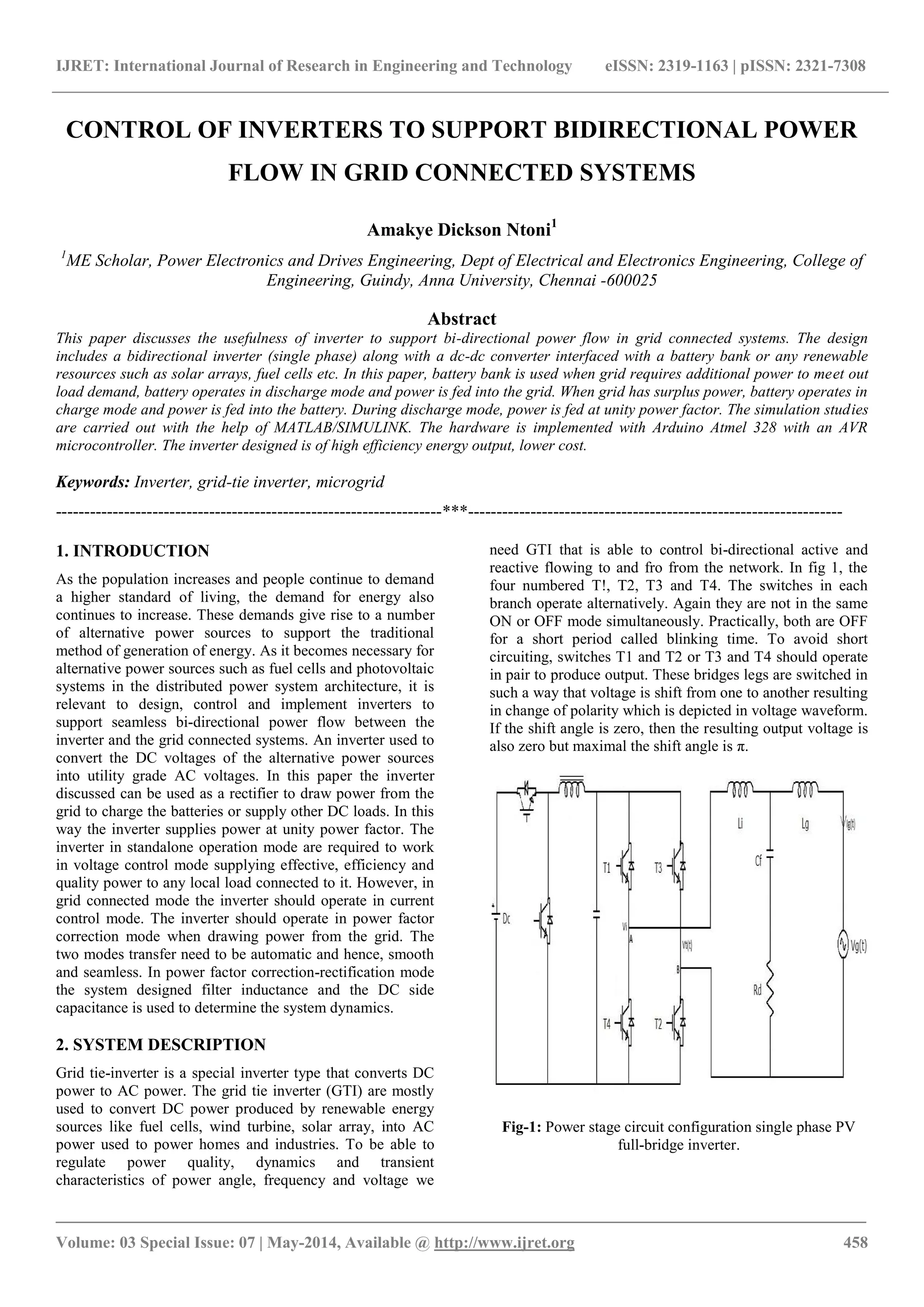
reactive flowing to and fro from the network. In fig 1, the
four numbered T!, T2, T3 and T4. The switches in each
branch operate alternatively. Again they are not in the same
ON or OFF mode simultaneously. Practically, both are OFF
for a short period called blinking time. To avoid short
circuiting, switches T1 and T2 or T3 and T4 should operate
in pair to produce output. These bridges legs are switched in
such a way that voltage is shift from one to another resulting
in change of polarity which is depicted in voltage waveform.
If the shift angle is zero, then the resulting output voltage is
also zero but maximal the shift angle is π.
Fig-1: Power stage circuit configuration single phase PV
full-bridge inverter.
IJRET: International Journal of Research in Engineering and Technology eISSN: 2319-1163 | pISSN: 2321-7308
_______________________________________________________________________________________
Volume: 03 Special Issue: 07 | May-2014, Available @ http://www.ijret.org 459
The reason of this full bridge single phase inverter is that it
provides voltage across the inductor which in turns, generate
current as express by the equation below:
Where VL and C represent the voltage the voltage across the
inductor and the integration constant respectively
For low voltage application CSI voltage is not suitable
hence additional buck converter is used. For minimizing CSI
switching losses, new reverse blocking IGBT techniques are
employed. [5], this reduces the power loss and increases
efficiency of system.
HF link inverter is used between DC-DC converters. The
inverter converts direct input voltage into an HFs square
wave which is rectified and subsequently filtered using LPF
low pass output is a high-level direct voltage that is
converted into a low frequency wave.
The Fourier series output voltage of square wave inverter is
given:
Where
Therefore;
For modified square wave, the Fourier series output voltage
is express as:
3. INVERTER SPECIFICATION
The inverter specification is presented in th Table 1. As the
design primarily focuses on the control and the grid
synchronization method of the inverter, the efficiency target
of the inverter is not specified because it is outside of the
scope.
Table- 1: Inverter Specifications
Assuming the grid voltage and the grid current are:
Vg(t)=Ṽgcos(ωgt) [5]
Ig(t)= Îgcos(ωgt − φ) [6]
Then the instantaneous output power can be easily obtained
as:
Pout (t) = Ṽg Îgcos(ωgt)cos(ωgt − φ) [7]
= ṼrmsÎgrms + ṼrmsÎgrmscos(2ωgt−φ)
This can be rewritten to be:
Pout (t) = Scosφ + Scos(2ωgt − φ) [8]
Where S denote apparent power which has a unit of VA
4. COMPUTER SIMULATION
The simulation tool used is MATLAB/SIMULINK. The
DC/DC converter converters the non constants dc voltage
coming from the renewable sources into a constant 24V DC
voltage and subsequently supply it to the inverter. The
inverter then converts this DC voltage to AC and feed to the
grid at unity power factor. Initially Single phase inverter is
designed with Resistive load is shown in fig-3.
The closed loop simulation is also realized
IJRET: International Journal of Research in Engineering and Technology eISSN: 2319-1163 | pISSN: 2321-7308
_______________________________________________________________________________________
Volume: 03 Special Issue: 07 | May-2014, Available @ http://www.ijret.org 460
Fig-2: Structure of Matlab/SimulinkSimulation
The current output il from the circuit is compared with the
reference signal for which current error icr is generated. The
switch control logic is produced when current error signal
icr is fed to the current control block. The output current is
controlled by the power circuit connected to it by the switch
control lines.
The different simulation values are defined by the following
equation:
Vg = Ag sin(2πfgt) [9]
VR= AR sin(2πfRt + ϕ) [10]
Fig-3: Single phase inverter modeling
Fig-4: Gate pulses for MOSFET
Fig-5: Inverter with Resistive load
Fig-6: Grid voltage and current waveform
5. HARDWARE DESCRIPTION
The overall hardware setup is shown in fig-8. DC-Dc
convreter is fed from a fluctuating Dc source to be converted
to fixed Dc value of 24V. this falls to be the input for the
inverter. The H-bridge inverter is made up of four IRF40 n-
MOSFET(n-channel enhancement). Th MOSFET witches
are rated for 60V-100V for voltage and 27A for current,
with fast switching time of 25nanoseconds for rising time
and 25nanoseconds for falling times. The switches have
high efficiency with less power disipation.
The IFR540 MOSFET switche are driven using IR2110
drivers. The PWM gate pulses to drive the MOSFET are
generated using Arduino ATmega 328 microprocesor which
turns at a clock peed of 16MHz. The transistors and Op-
Amps are used to convert two PWM signals comin from the
arduino microcontroller into four signals to drive the
MOSFET. Electrical isloation of power electronics voltage
circuits were done with the aid of optocoupler 6N25. The
inverter is connected to an inductor and capacitor. The cut
off frquency of the LC filter is given by:
For L=37mH and C=2.6μF, Fc=513Hz
IJRET: International Journal of Research in Engineering and Technology eISSN: 2319-1163 | pISSN: 2321-7308
_______________________________________________________________________________________
Volume: 03 Special Issue: 07 | May-2014, Available @ http://www.ijret.org 461
The resulting output impedance (Z) of the filter is given by
With the same values for L and C, Z= 4.26Ω
In order to improve the output waveform of the grid and to
maximize the power transfer to the grid, a damping resistor
is connected in parallel with the capacitor to match the input
impedance of the grid.
The inverter is used tracks both the phase and frequency of
the grid waveform. The tracked waveform is used to
generate output signals to drive the H-bridge‟s low and high
side switches.
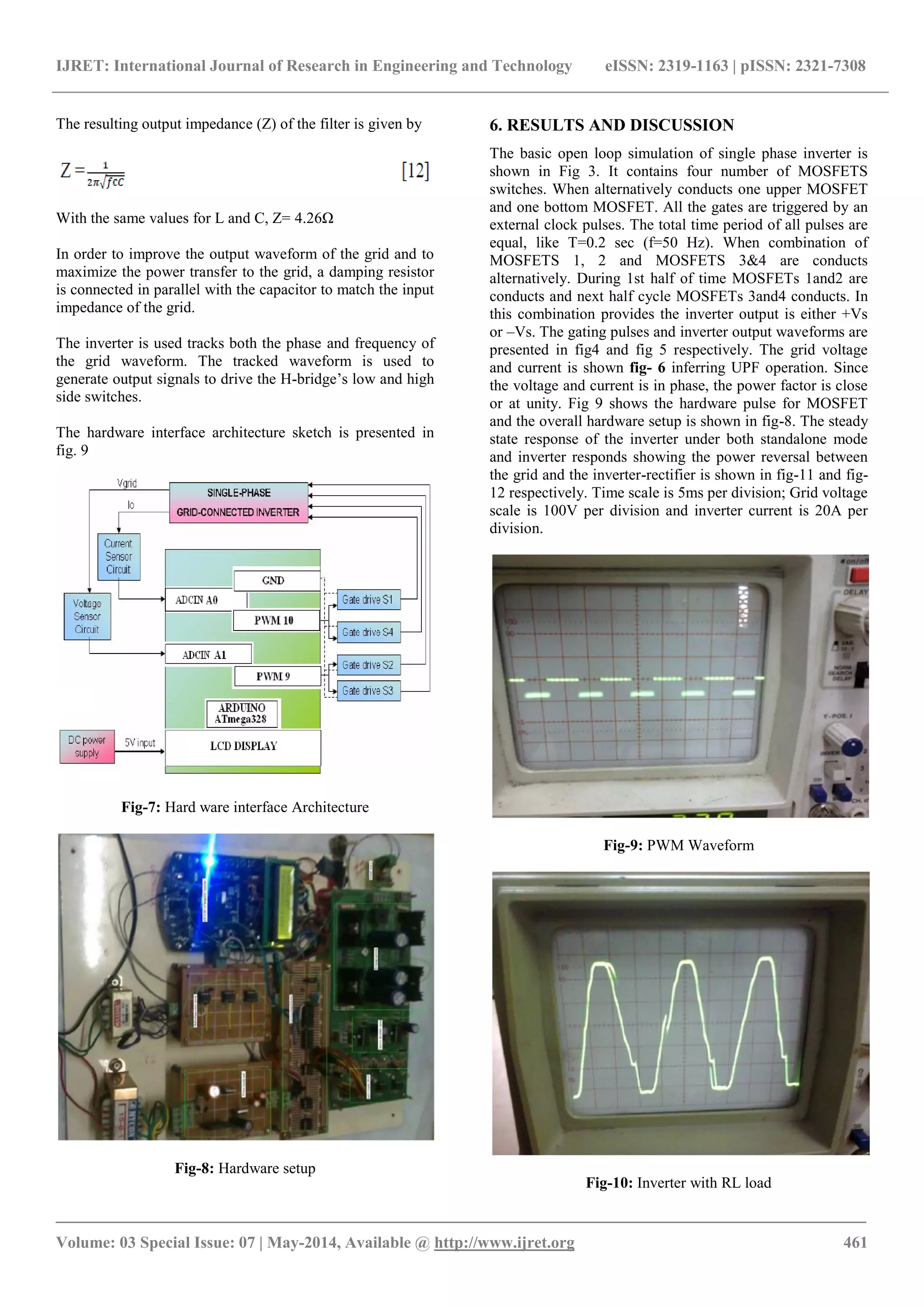
The hardware interface architecture sketch is presented in
fig. 9
Fig-7: Hard ware interface Architecture
Fig-8: Hardware setup
6. RESULTS AND DISCUSSION
The basic open loop simulation of single phase inverter is
shown in Fig 3. It contains four number of MOSFETS
switches. When alternatively conducts one upper MOSFET
and one bottom MOSFET. All the gates are triggered by an
external clock pulses. The total time period of all pulses are
equal, like T=0.2 sec (f=50 Hz). When combination of
MOSFETS 1, 2 and MOSFETS 3&4 are conducts
alternatively. During 1st half of time MOSFETs 1and2 are
conducts and next half cycle MOSFETs 3and4 conducts. In
this combination provides the inverter output is either +Vs
or –Vs. The gating pulses and inverter output waveforms are
presented in fig4 and fig 5 respectively. The grid voltage
and current is shown fig- 6 inferring UPF operation. Since
the voltage and current is in phase, the power factor is close
or at unity. Fig 9 shows the hardware pulse for MOSFET
and the overall hardware setup is shown in fig-8. The steady
state response of the inverter under both standalone mode
and inverter responds showing the power reversal between
the grid and the inverter-rectifier is shown in fig-11 and fig-
12 respectively. Time scale is 5ms per division; Grid voltage
scale is 100V per division and inverter current is 20A per
division.
Fig-9: PWM Waveform
Fig-10: Inverter with RL load
IJRET: International Journal of Research in Engineering and Technology eISSN: 2319-1163 | pISSN: 2321-7308
_______________________________________________________________________________________
Volume: 03 Special Issue: 07 | May-2014, Available @ http://www.ijret.org 462
Fig-11: Grid voltage and current output.
Fig-12: Inverter response showing power reversal between
grid and inverter-rectifier.
7. CONCLUSIONS
Design of inverters to support bidirectional power flow in
grid connected inverter systems has been presented. The
frequency, amplitude and phase the inverter output signal
are synchronizing with that the grid voltage signal. An
arduino Atmel microcontroller is used to control the single
phase inverter switches. It is deduced that the grid tied
inverter is able to produce an Ac waveform which is
synchronized with the grid.
The setup is capable of controlling both the inverter‟s real
and reactive power output. The LC filter of the inverter is
capable of removing most the noise, and provides better
filter structure required for smooth output waveforms
REFERENCES
[1]. D.M. Baker, V.G. Agelidis, C.V. Nayer, “A comparison
of tri-level and bi-level current controlled grid-connected
single-phase full-bridge inverters", ISlE '97. Proceedings of
the IEEE International Symposium on Industrial Electronics,
Volume: 2, 1997, page(s): 463 -468.
[2]. IOANNIDIS, G., XANTHOULIS, E., and MANIAS,
S.N.: „A novel uninterruptible power supply system with
sinusoidal input–output characteristics and simplified
control circuit‟. Proceedings of the IEEE International
Symposium on lndustdal electronics, 1995, Vol. 2, pp.
[3]. D.H. Moore, H.M. Abdar, A. Chakraverty, J.M.Murray,
K.A. Loparo, Grid of the Future Laboratory Demonstration
System, Submitted to Energy Tech 2012 Conference.603–
609
[4]. Klumpner, C. “A New Single-Stage Current Source
Inverter for Photovoltaic and Fuel Cell Applications using
Reverse Blocking IGBTs.” Power Electronics Specialists
Conference, 2007. PESC 1683 -1689, IEEE 2007
[5]. BOSE, B.K., SZCZESNY, P.M., and STEIGERWALD,
R.: „Micro- computer control of a residential photovoltaic
power conditioning sys- tem‟, IEEE Trans. Ind. Appl., IEEE
Trans. Ind. Appl., 21, [5], pp.1182–1191
[6]. HORTA, H.S., and CARDENNAS, G.V.M.: „DC-AC
converter with high frequency DC link for UPS
applications‟. Proceedings of the 3rd International
Conference on Power electronics, 1994, pp. 125–130
[7]. Carbone, R., “Grid-connected photovoltaic systems with
energy storage”. In Clean Electrical Power, 2009
International Conference, 760-767
[8]. A.Nachiappan, K.Sundararajan, V Malarselvam,
“Current controlled voltage source inverter using Hysteresis
controller and PI controller”, IEEE Int. Conf. on Power,
Signals, Controls and Computation (EPSCICON), pp.1- 6,
20129.
[9]. Philip P. Barker, James M. Bing, “Advances in Solar
Photovoltaic Technology: An Applications Perspective”,
Power Engineering Society General Meeting, IEEE, pp.
1955- 1960 Vol. 2 2005.
[10]. Feng Gao, Chao Liang, Poh Chiang Loh, Frede
Blaabjerg, “Buck–Boost Current-Source Inverters With
Diode-Inductor Network”, IEEE Transactions On Industry
Applications, Vol. 45, No. 2, March/April 2009.
[11]. F. Flinders, S. Senini and W. Oghanna, “Power
electronic Simulation laboratory using “Simulink”
Dynamics Systems Analysis Package, ZMACS, July1993,
pp643-650
[12]. M.H.Rashid, "Power Electronics Circuit Device and
Application", 3rd Ed. New Delhi, India, Pearson Education,
2011, pp. 352-430
BIOGRAPHIES
Amakye Dickson Ntoni received the B.E
degree in ECE from All Nations University
College, Koforidua, Ghana-West Africa. He
is currently pursuing ME Power Electronics
and Drives in Electrical Dept. at Anna
University (CEG) India. His interests are
wireless communications, power converters and inverters.
He also has interest in power systems analysis and control.

Control of inverters to support bidirectional power flow in grid connected systems

  • 1.
    IJRET: International Journalof Research in Engineering and Technology eISSN: 2319-1163 | pISSN: 2321-7308 _______________________________________________________________________________________ Volume: 03 Special Issue: 07 | May-2014, Available @ http://www.ijret.org 458 CONTROL OF INVERTERS TO SUPPORT BIDIRECTIONAL POWER FLOW IN GRID CONNECTED SYSTEMS Amakye Dickson Ntoni1 1 ME Scholar, Power Electronics and Drives Engineering, Dept of Electrical and Electronics Engineering, College of Engineering, Guindy, Anna University, Chennai -600025 Abstract This paper discusses the usefulness of inverter to support bi-directional power flow in grid connected systems. The design includes a bidirectional inverter (single phase) along with a dc-dc converter interfaced with a battery bank or any renewable resources such as solar arrays, fuel cells etc. In this paper, battery bank is used when grid requires additional power to meet out load demand, battery operates in discharge mode and power is fed into the grid. When grid has surplus power, battery operates in charge mode and power is fed into the battery. During discharge mode, power is fed at unity power factor. The simulation studies are carried out with the help of MATLAB/SIMULINK. The hardware is implemented with Arduino Atmel 328 with an AVR microcontroller. The inverter designed is of high efficiency energy output, lower cost. Keywords: Inverter, grid-tie inverter, microgrid --------------------------------------------------------------------***------------------------------------------------------------------ 1. INTRODUCTION As the population increases and people continue to demand a higher standard of living, the demand for energy also continues to increase. These demands give rise to a number of alternative power sources to support the traditional method of generation of energy. As it becomes necessary for alternative power sources such as fuel cells and photovoltaic systems in the distributed power system architecture, it is relevant to design, control and implement inverters to support seamless bi-directional power flow between the inverter and the grid connected systems. An inverter used to convert the DC voltages of the alternative power sources into utility grade AC voltages. In this paper the inverter discussed can be used as a rectifier to draw power from the grid to charge the batteries or supply other DC loads. In this way the inverter supplies power at unity power factor. The inverter in standalone operation mode are required to work in voltage control mode supplying effective, efficiency and quality power to any local load connected to it. However, in grid connected mode the inverter should operate in current control mode. The inverter should operate in power factor correction mode when drawing power from the grid. The two modes transfer need to be automatic and hence, smooth and seamless. In power factor correction-rectification mode the system designed filter inductance and the DC side capacitance is used to determine the system dynamics. 2. SYSTEM DESCRIPTION Grid tie-inverter is a special inverter type that converts DC power to AC power. The grid tie inverter (GTI) are mostly used to convert DC power produced by renewable energy sources like fuel cells, wind turbine, solar array, into AC power used to power homes and industries. To be able to regulate power quality, dynamics and transient characteristics of power angle, frequency and voltage we need GTI that is able to control bi-directional active and reactive flowing to and fro from the network. In fig 1, the four numbered T!, T2, T3 and T4. The switches in each branch operate alternatively. Again they are not in the same ON or OFF mode simultaneously. Practically, both are OFF for a short period called blinking time. To avoid short circuiting, switches T1 and T2 or T3 and T4 should operate in pair to produce output. These bridges legs are switched in such a way that voltage is shift from one to another resulting in change of polarity which is depicted in voltage waveform. If the shift angle is zero, then the resulting output voltage is also zero but maximal the shift angle is π. Fig-1: Power stage circuit configuration single phase PV full-bridge inverter.
  • 2.
    IJRET: International Journalof Research in Engineering and Technology eISSN: 2319-1163 | pISSN: 2321-7308 _______________________________________________________________________________________ Volume: 03 Special Issue: 07 | May-2014, Available @ http://www.ijret.org 459 The reason of this full bridge single phase inverter is that it provides voltage across the inductor which in turns, generate current as express by the equation below: Where VL and C represent the voltage the voltage across the inductor and the integration constant respectively For low voltage application CSI voltage is not suitable hence additional buck converter is used. For minimizing CSI switching losses, new reverse blocking IGBT techniques are employed. [5], this reduces the power loss and increases efficiency of system. HF link inverter is used between DC-DC converters. The inverter converts direct input voltage into an HFs square wave which is rectified and subsequently filtered using LPF low pass output is a high-level direct voltage that is converted into a low frequency wave. The Fourier series output voltage of square wave inverter is given: Where Therefore; For modified square wave, the Fourier series output voltage is express as: 3. INVERTER SPECIFICATION The inverter specification is presented in th Table 1. As the design primarily focuses on the control and the grid synchronization method of the inverter, the efficiency target of the inverter is not specified because it is outside of the scope. Table- 1: Inverter Specifications Assuming the grid voltage and the grid current are: Vg(t)=Ṽgcos(ωgt) [5] Ig(t)= Îgcos(ωgt − φ) [6] Then the instantaneous output power can be easily obtained as: Pout (t) = Ṽg Îgcos(ωgt)cos(ωgt − φ) [7] = ṼrmsÎgrms + ṼrmsÎgrmscos(2ωgt−φ) This can be rewritten to be: Pout (t) = Scosφ + Scos(2ωgt − φ) [8] Where S denote apparent power which has a unit of VA 4. COMPUTER SIMULATION The simulation tool used is MATLAB/SIMULINK. The DC/DC converter converters the non constants dc voltage coming from the renewable sources into a constant 24V DC voltage and subsequently supply it to the inverter. The inverter then converts this DC voltage to AC and feed to the grid at unity power factor. Initially Single phase inverter is designed with Resistive load is shown in fig-3. The closed loop simulation is also realized
  • 3.
    IJRET: International Journalof Research in Engineering and Technology eISSN: 2319-1163 | pISSN: 2321-7308 _______________________________________________________________________________________ Volume: 03 Special Issue: 07 | May-2014, Available @ http://www.ijret.org 460 Fig-2: Structure of Matlab/SimulinkSimulation The current output il from the circuit is compared with the reference signal for which current error icr is generated. The switch control logic is produced when current error signal icr is fed to the current control block. The output current is controlled by the power circuit connected to it by the switch control lines. The different simulation values are defined by the following equation: Vg = Ag sin(2πfgt) [9] VR= AR sin(2πfRt + ϕ) [10] Fig-3: Single phase inverter modeling Fig-4: Gate pulses for MOSFET Fig-5: Inverter with Resistive load Fig-6: Grid voltage and current waveform 5. HARDWARE DESCRIPTION The overall hardware setup is shown in fig-8. DC-Dc convreter is fed from a fluctuating Dc source to be converted to fixed Dc value of 24V. this falls to be the input for the inverter. The H-bridge inverter is made up of four IRF40 n- MOSFET(n-channel enhancement). Th MOSFET witches are rated for 60V-100V for voltage and 27A for current, with fast switching time of 25nanoseconds for rising time and 25nanoseconds for falling times. The switches have high efficiency with less power disipation. The IFR540 MOSFET switche are driven using IR2110 drivers. The PWM gate pulses to drive the MOSFET are generated using Arduino ATmega 328 microprocesor which turns at a clock peed of 16MHz. The transistors and Op- Amps are used to convert two PWM signals comin from the arduino microcontroller into four signals to drive the MOSFET. Electrical isloation of power electronics voltage circuits were done with the aid of optocoupler 6N25. The inverter is connected to an inductor and capacitor. The cut off frquency of the LC filter is given by: For L=37mH and C=2.6μF, Fc=513Hz
  • 4.
    IJRET: International Journalof Research in Engineering and Technology eISSN: 2319-1163 | pISSN: 2321-7308 _______________________________________________________________________________________ Volume: 03 Special Issue: 07 | May-2014, Available @ http://www.ijret.org 461 The resulting output impedance (Z) of the filter is given by With the same values for L and C, Z= 4.26Ω In order to improve the output waveform of the grid and to maximize the power transfer to the grid, a damping resistor is connected in parallel with the capacitor to match the input impedance of the grid. The inverter is used tracks both the phase and frequency of the grid waveform. The tracked waveform is used to generate output signals to drive the H-bridge‟s low and high side switches. The hardware interface architecture sketch is presented in fig. 9 Fig-7: Hard ware interface Architecture Fig-8: Hardware setup 6. RESULTS AND DISCUSSION The basic open loop simulation of single phase inverter is shown in Fig 3. It contains four number of MOSFETS switches. When alternatively conducts one upper MOSFET and one bottom MOSFET. All the gates are triggered by an external clock pulses. The total time period of all pulses are equal, like T=0.2 sec (f=50 Hz). When combination of MOSFETS 1, 2 and MOSFETS 3&4 are conducts alternatively. During 1st half of time MOSFETs 1and2 are conducts and next half cycle MOSFETs 3and4 conducts. In this combination provides the inverter output is either +Vs or –Vs. The gating pulses and inverter output waveforms are presented in fig4 and fig 5 respectively. The grid voltage and current is shown fig- 6 inferring UPF operation. Since the voltage and current is in phase, the power factor is close or at unity. Fig 9 shows the hardware pulse for MOSFET and the overall hardware setup is shown in fig-8. The steady state response of the inverter under both standalone mode and inverter responds showing the power reversal between the grid and the inverter-rectifier is shown in fig-11 and fig- 12 respectively. Time scale is 5ms per division; Grid voltage scale is 100V per division and inverter current is 20A per division. Fig-9: PWM Waveform Fig-10: Inverter with RL load
  • 5.
    IJRET: International Journalof Research in Engineering and Technology eISSN: 2319-1163 | pISSN: 2321-7308 _______________________________________________________________________________________ Volume: 03 Special Issue: 07 | May-2014, Available @ http://www.ijret.org 462 Fig-11: Grid voltage and current output. Fig-12: Inverter response showing power reversal between grid and inverter-rectifier. 7. CONCLUSIONS Design of inverters to support bidirectional power flow in grid connected inverter systems has been presented. The frequency, amplitude and phase the inverter output signal are synchronizing with that the grid voltage signal. An arduino Atmel microcontroller is used to control the single phase inverter switches. It is deduced that the grid tied inverter is able to produce an Ac waveform which is synchronized with the grid. The setup is capable of controlling both the inverter‟s real and reactive power output. The LC filter of the inverter is capable of removing most the noise, and provides better filter structure required for smooth output waveforms REFERENCES [1]. D.M. Baker, V.G. Agelidis, C.V. Nayer, “A comparison of tri-level and bi-level current controlled grid-connected single-phase full-bridge inverters", ISlE '97. Proceedings of the IEEE International Symposium on Industrial Electronics, Volume: 2, 1997, page(s): 463 -468. [2]. IOANNIDIS, G., XANTHOULIS, E., and MANIAS, S.N.: „A novel uninterruptible power supply system with sinusoidal input–output characteristics and simplified control circuit‟. Proceedings of the IEEE International Symposium on lndustdal electronics, 1995, Vol. 2, pp. [3]. D.H. Moore, H.M. Abdar, A. Chakraverty, J.M.Murray, K.A. Loparo, Grid of the Future Laboratory Demonstration System, Submitted to Energy Tech 2012 Conference.603– 609 [4]. Klumpner, C. “A New Single-Stage Current Source Inverter for Photovoltaic and Fuel Cell Applications using Reverse Blocking IGBTs.” Power Electronics Specialists Conference, 2007. PESC 1683 -1689, IEEE 2007 [5]. BOSE, B.K., SZCZESNY, P.M., and STEIGERWALD, R.: „Micro- computer control of a residential photovoltaic power conditioning sys- tem‟, IEEE Trans. Ind. Appl., IEEE Trans. Ind. Appl., 21, [5], pp.1182–1191 [6]. HORTA, H.S., and CARDENNAS, G.V.M.: „DC-AC converter with high frequency DC link for UPS applications‟. Proceedings of the 3rd International Conference on Power electronics, 1994, pp. 125–130 [7]. Carbone, R., “Grid-connected photovoltaic systems with energy storage”. In Clean Electrical Power, 2009 International Conference, 760-767 [8]. A.Nachiappan, K.Sundararajan, V Malarselvam, “Current controlled voltage source inverter using Hysteresis controller and PI controller”, IEEE Int. Conf. on Power, Signals, Controls and Computation (EPSCICON), pp.1- 6, 20129. [9]. Philip P. Barker, James M. Bing, “Advances in Solar Photovoltaic Technology: An Applications Perspective”, Power Engineering Society General Meeting, IEEE, pp. 1955- 1960 Vol. 2 2005. [10]. Feng Gao, Chao Liang, Poh Chiang Loh, Frede Blaabjerg, “Buck–Boost Current-Source Inverters With Diode-Inductor Network”, IEEE Transactions On Industry Applications, Vol. 45, No. 2, March/April 2009. [11]. F. Flinders, S. Senini and W. Oghanna, “Power electronic Simulation laboratory using “Simulink” Dynamics Systems Analysis Package, ZMACS, July1993, pp643-650 [12]. M.H.Rashid, "Power Electronics Circuit Device and Application", 3rd Ed. New Delhi, India, Pearson Education, 2011, pp. 352-430 BIOGRAPHIES Amakye Dickson Ntoni received the B.E degree in ECE from All Nations University College, Koforidua, Ghana-West Africa. He is currently pursuing ME Power Electronics and Drives in Electrical Dept. at Anna University (CEG) India. His interests are wireless communications, power converters and inverters. He also has interest in power systems analysis and control.