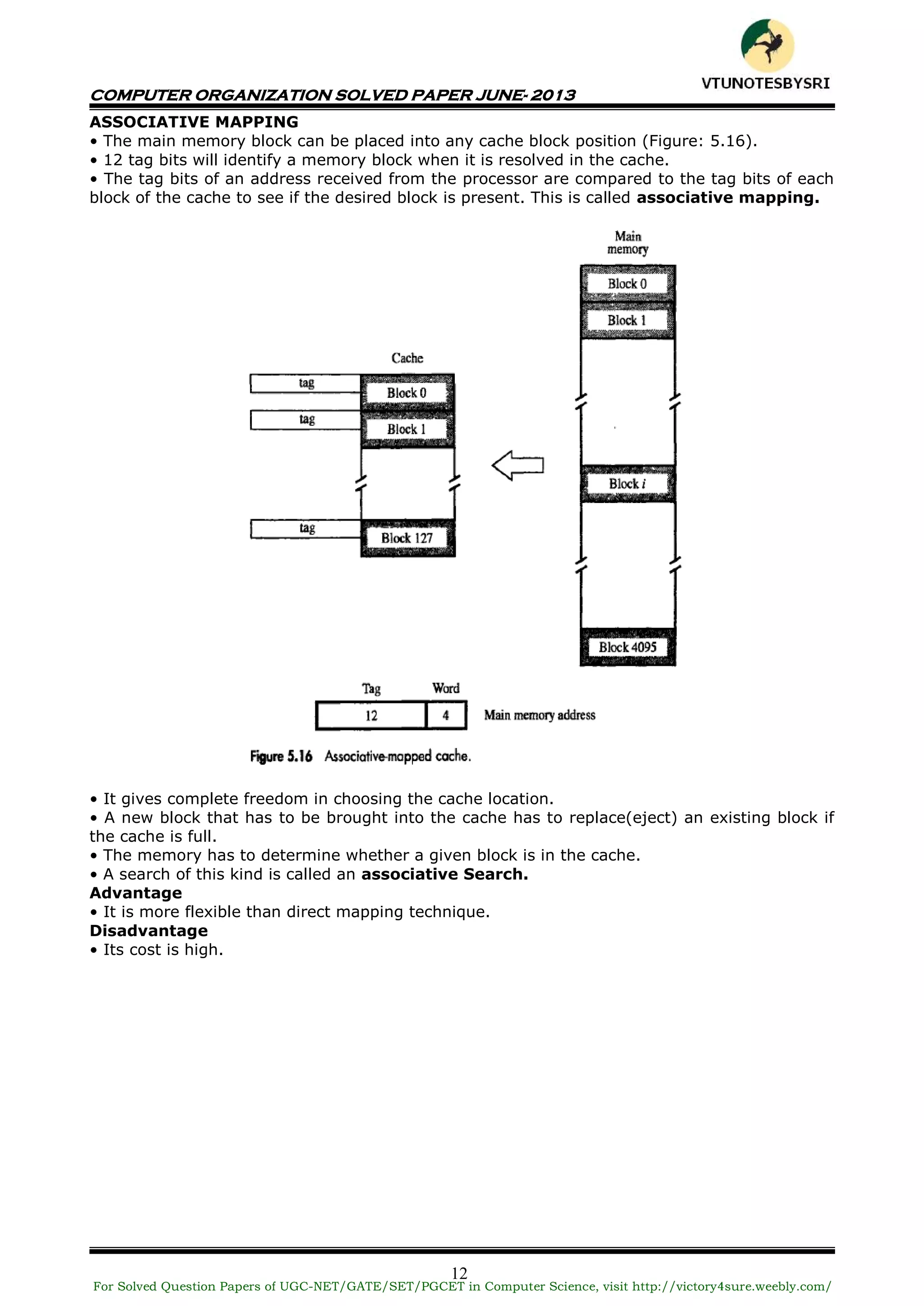
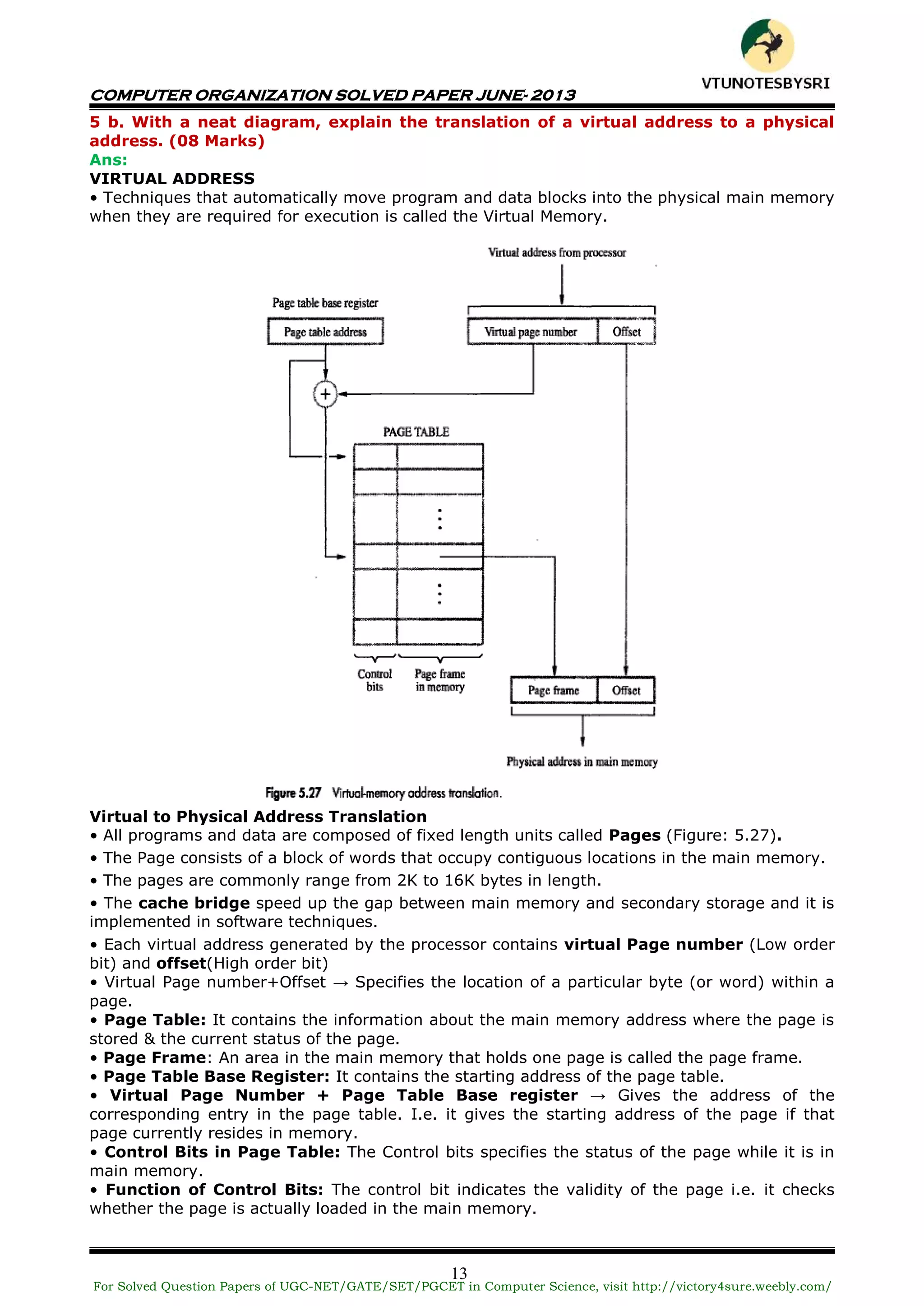
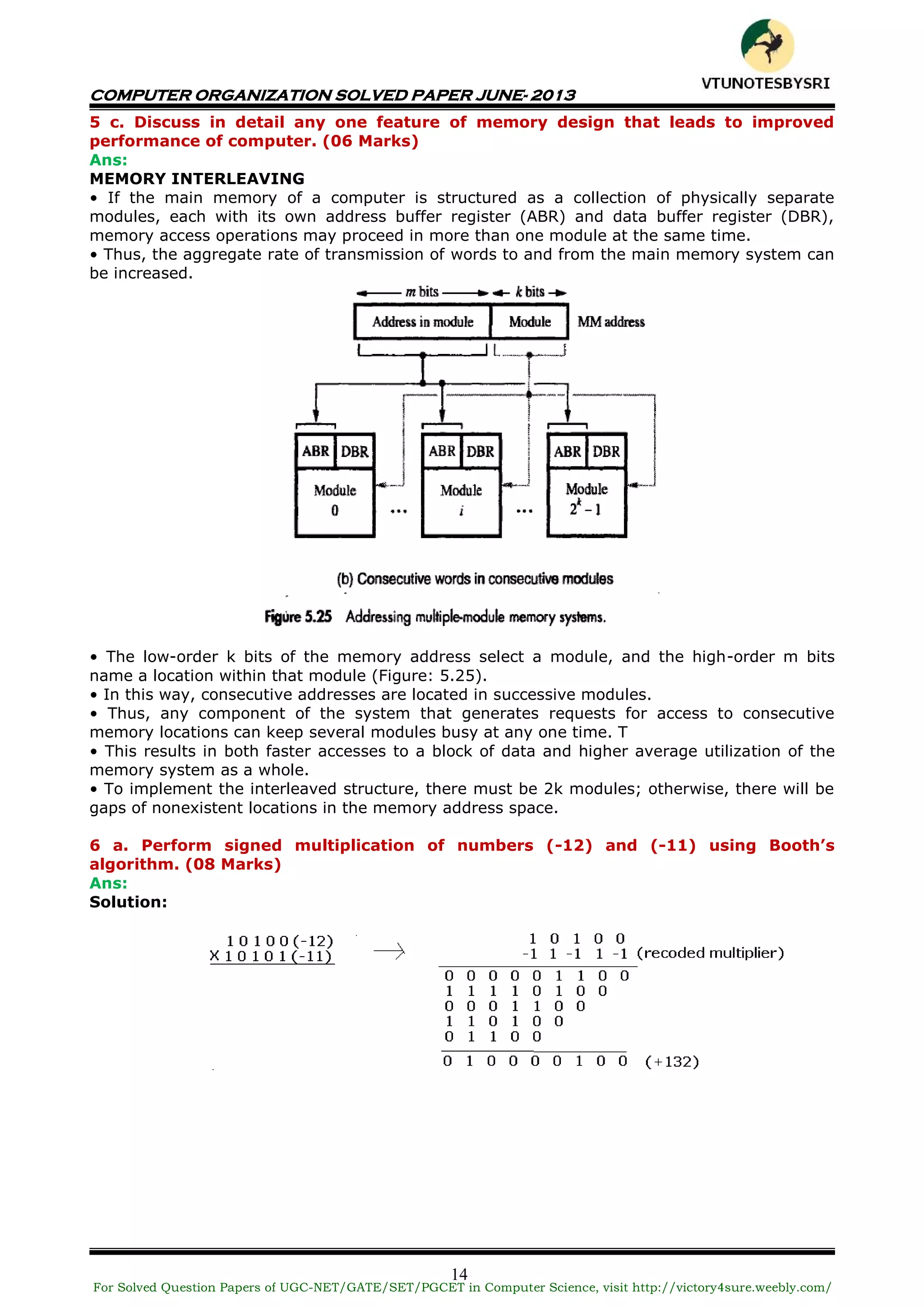
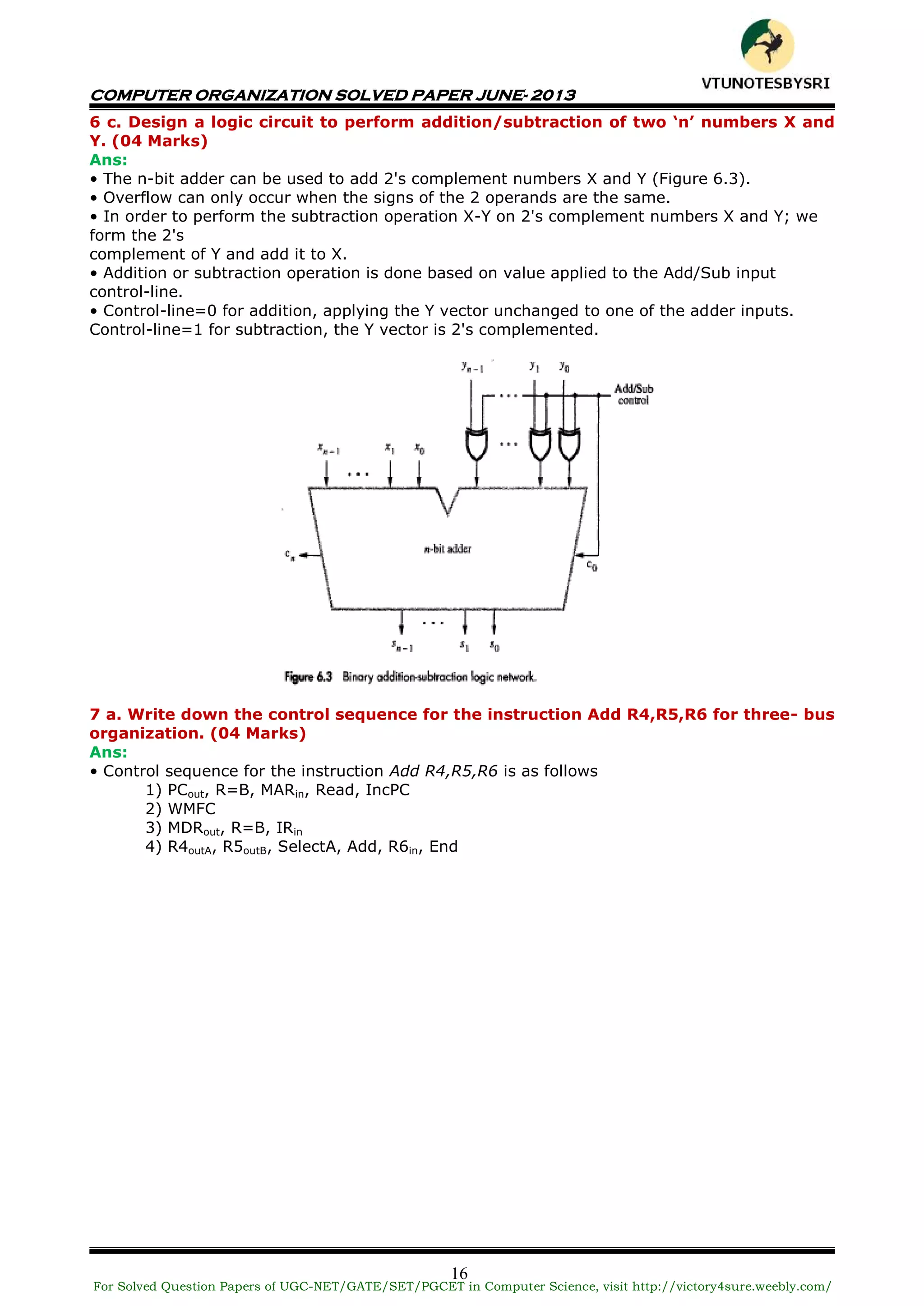
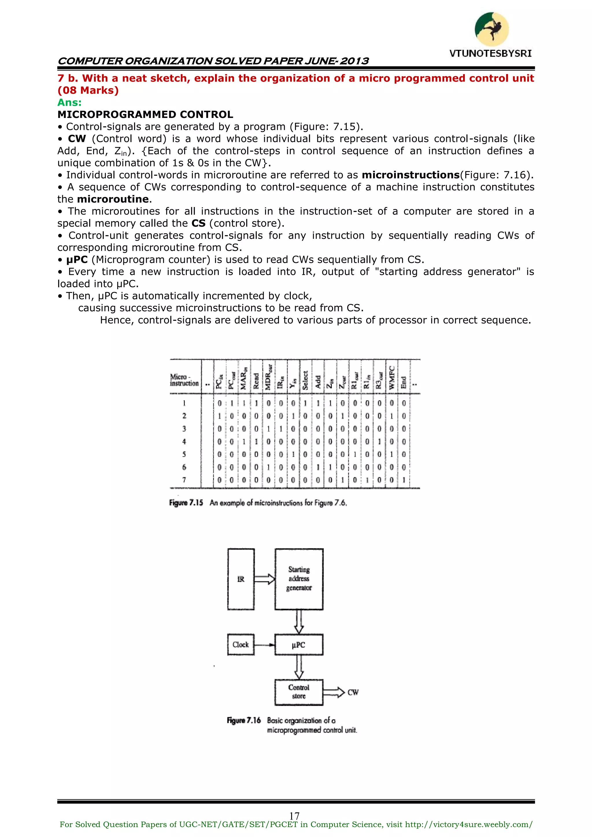
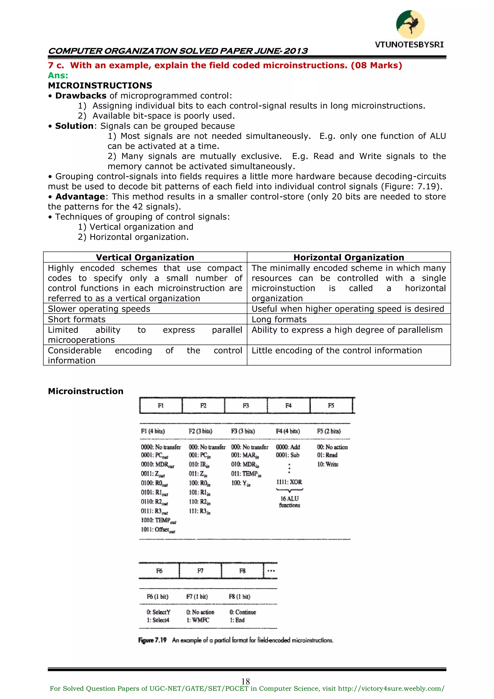
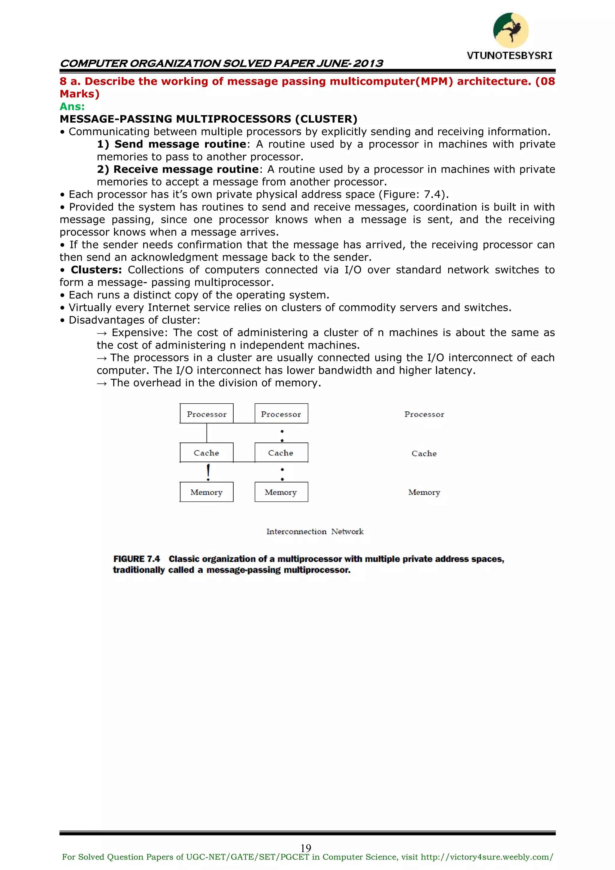
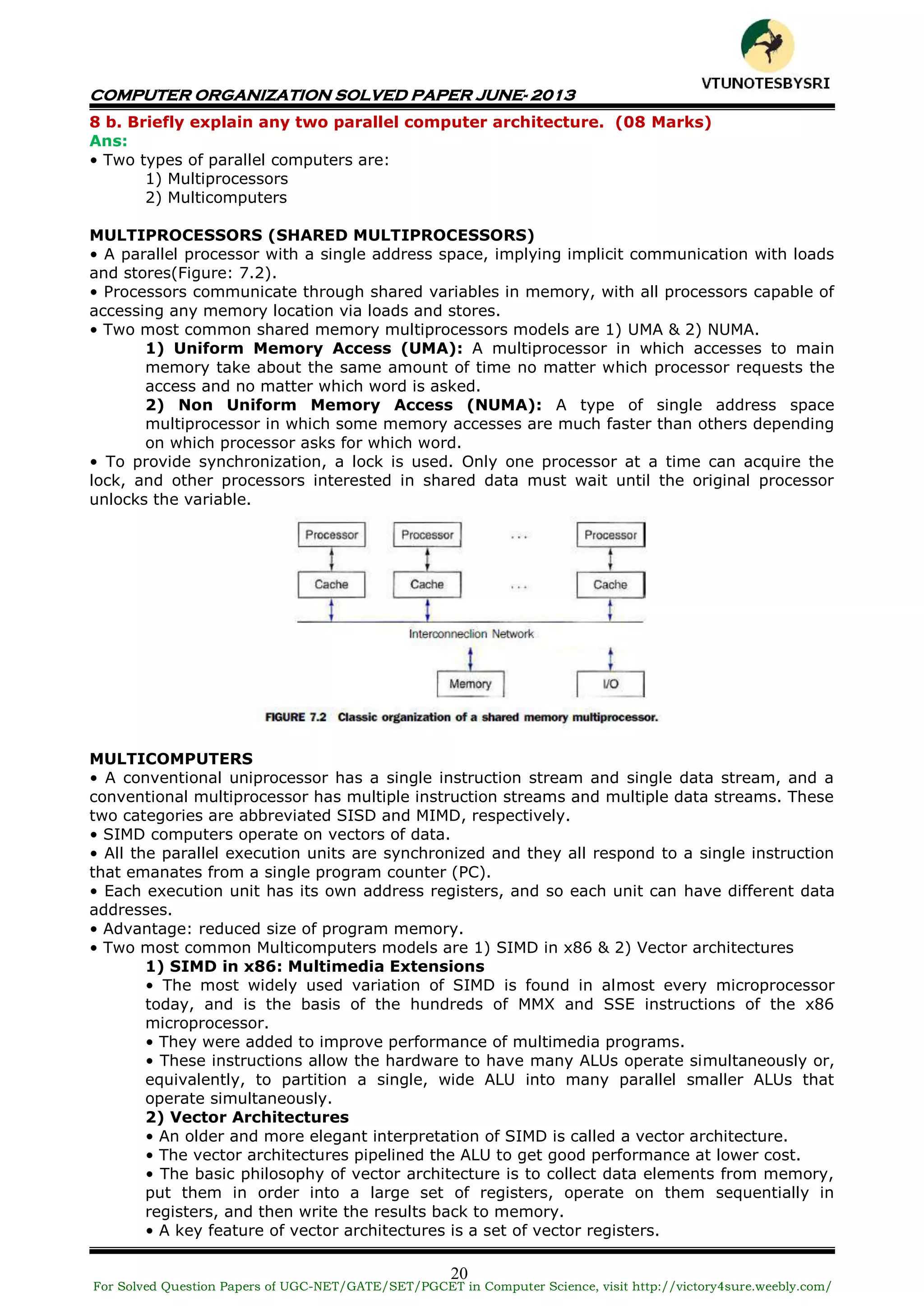
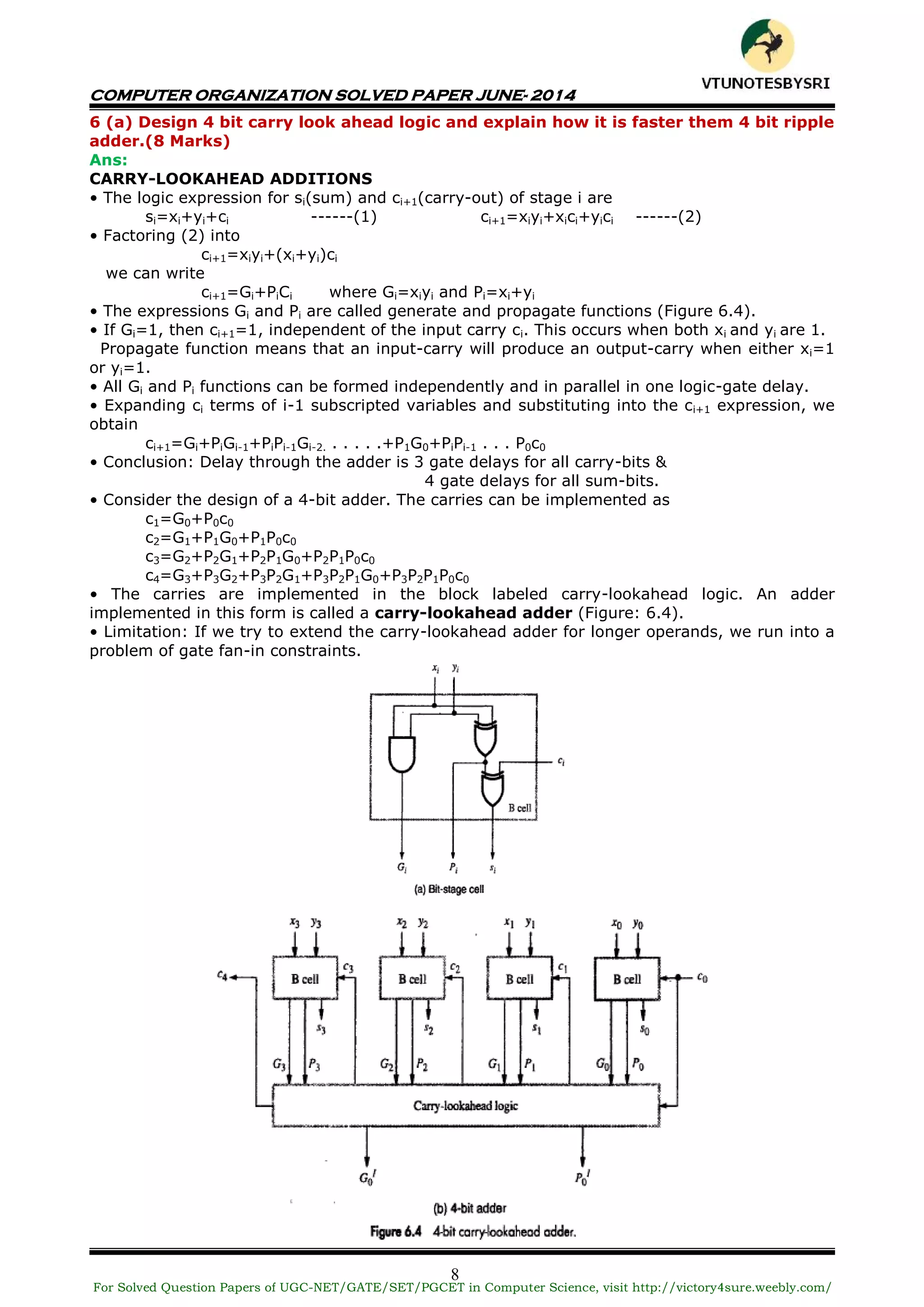
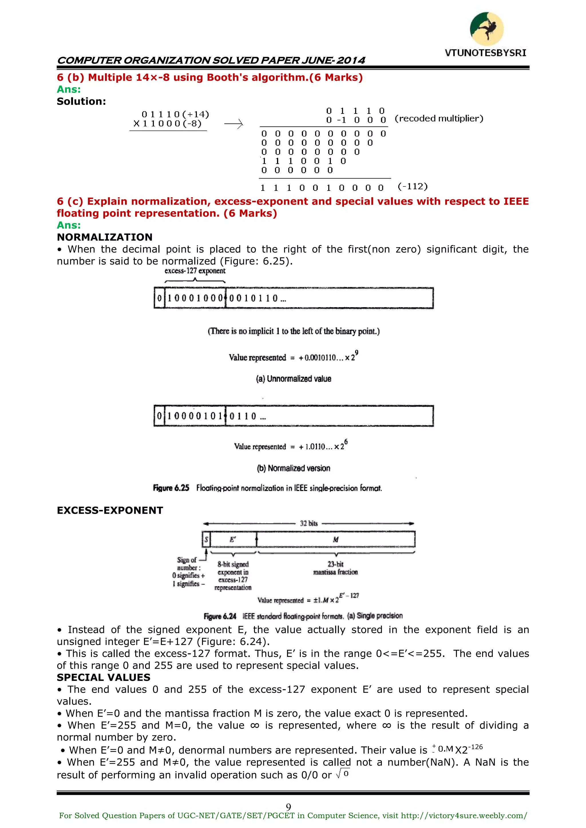
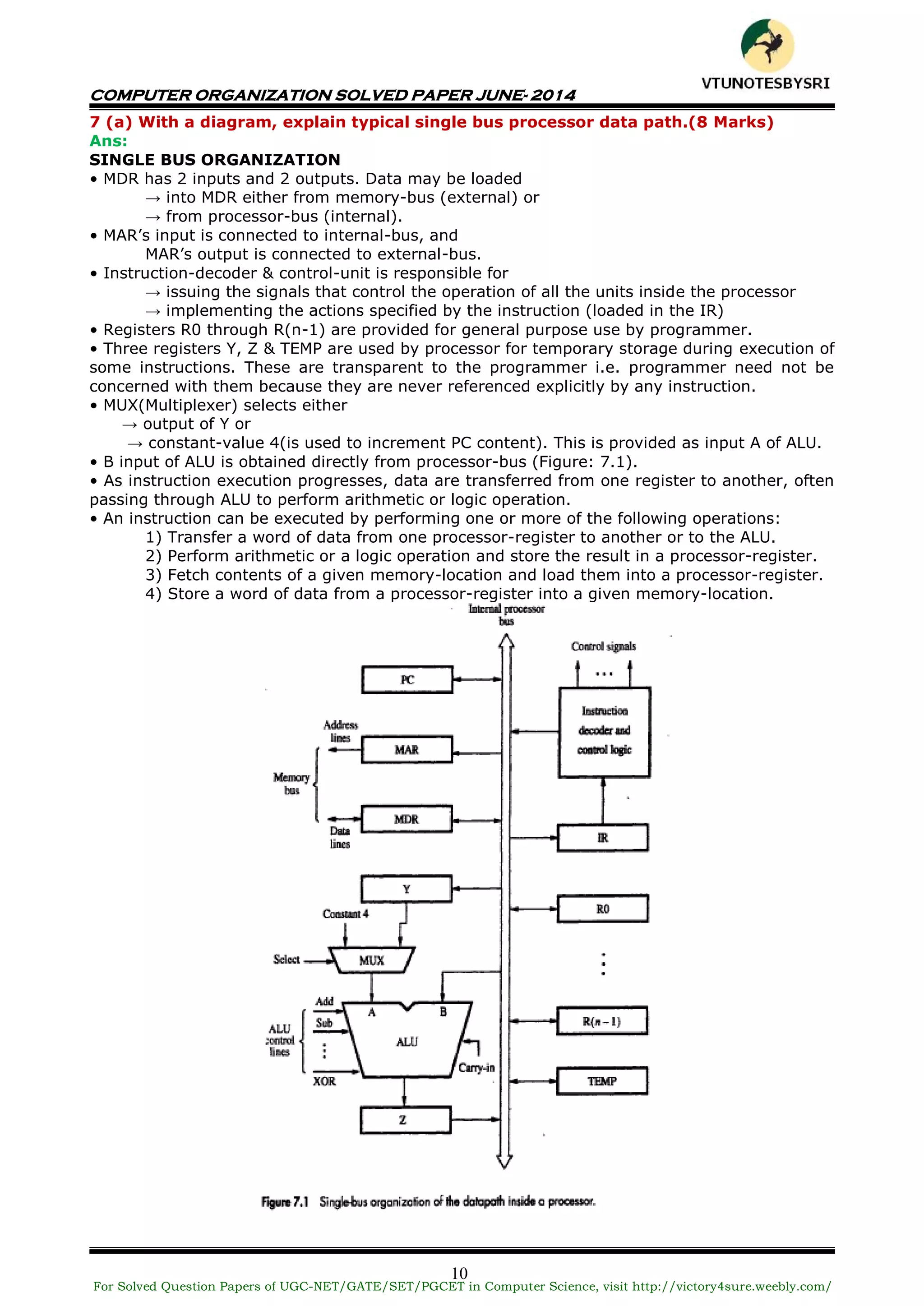
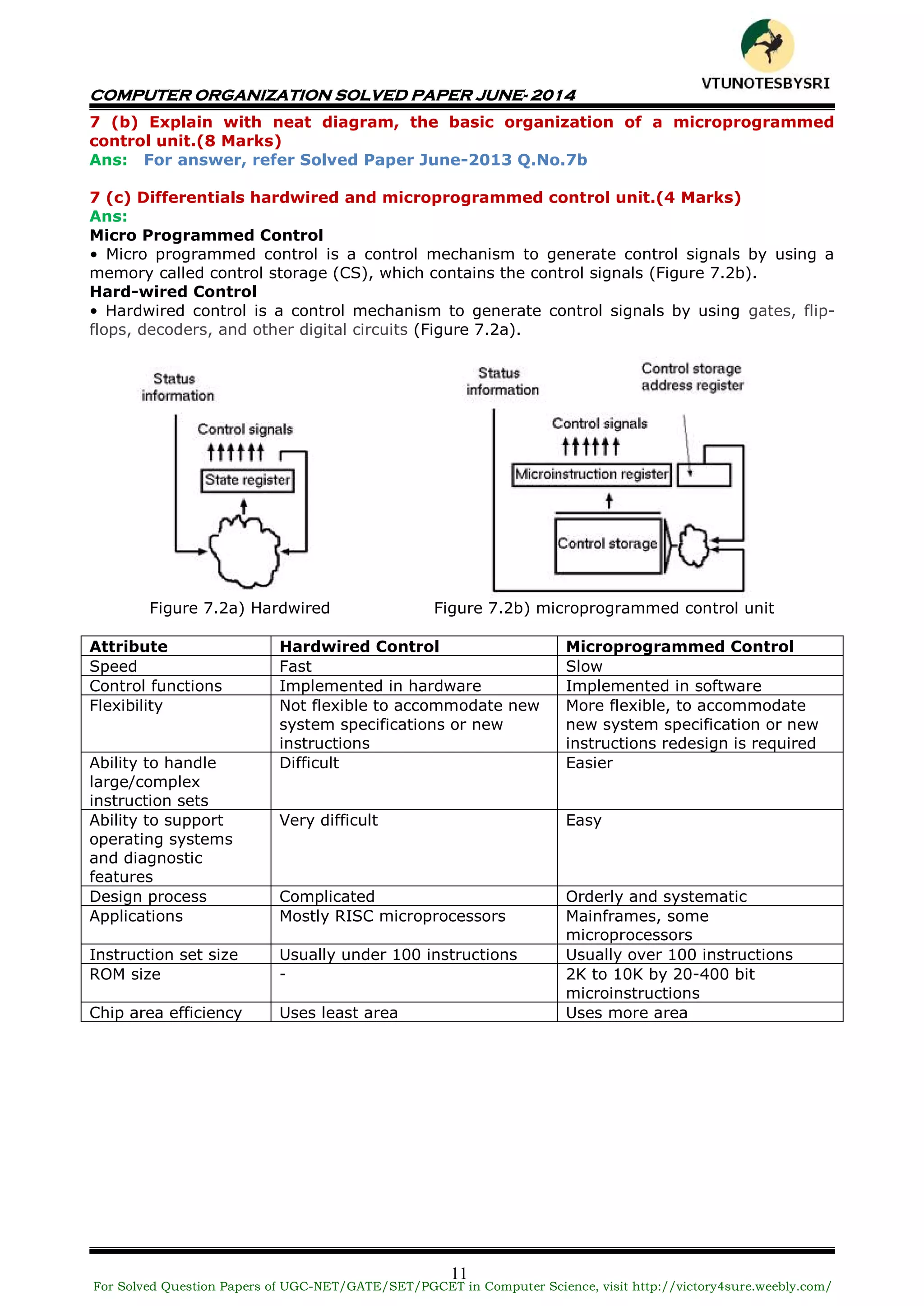
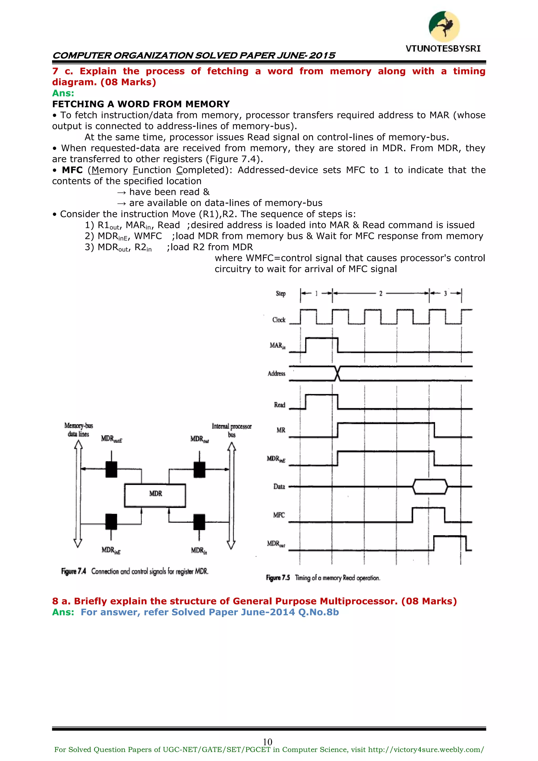
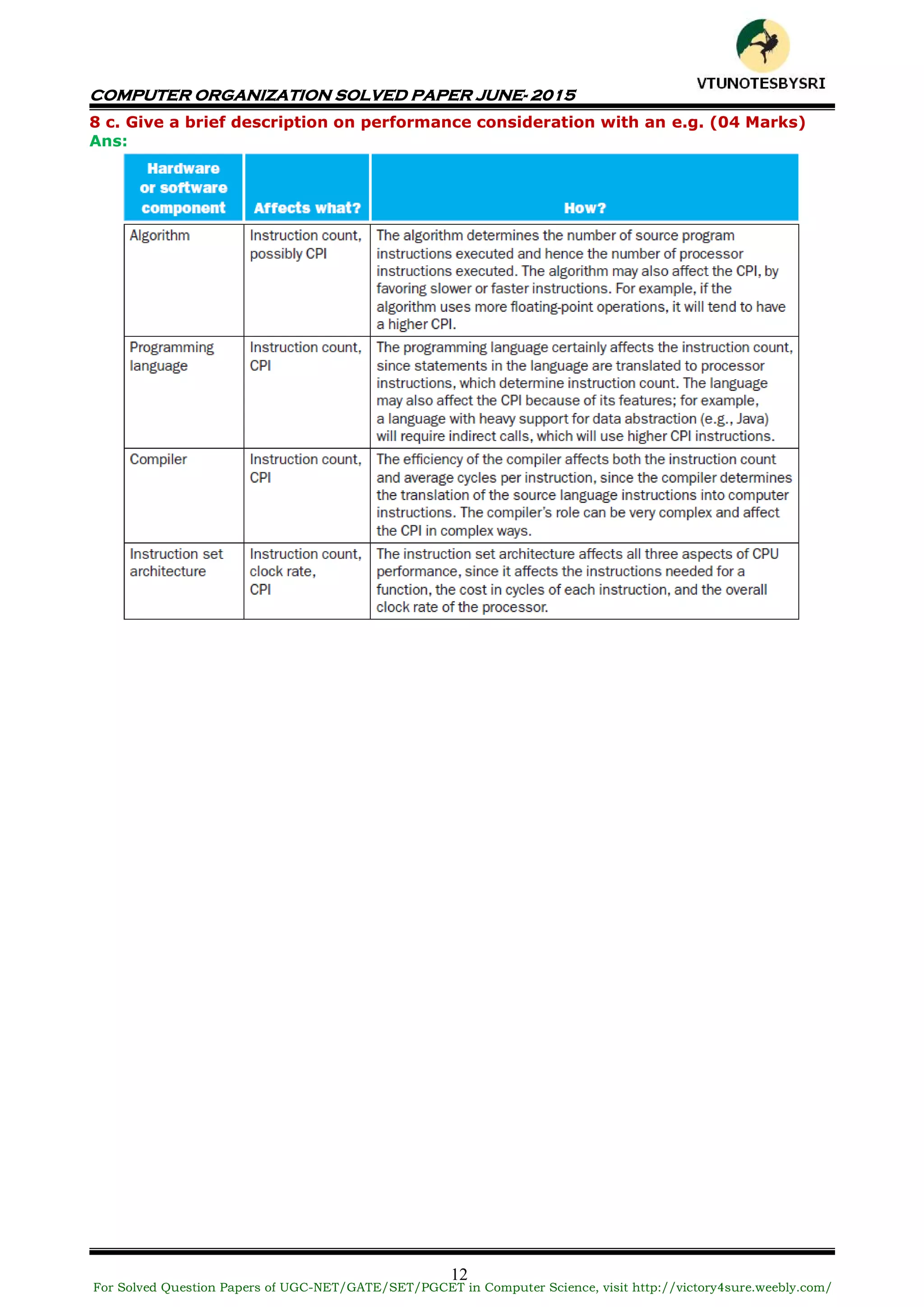
![COMPUTER ORGANIZATION SOLVED PAPER JUNE- 2013
3
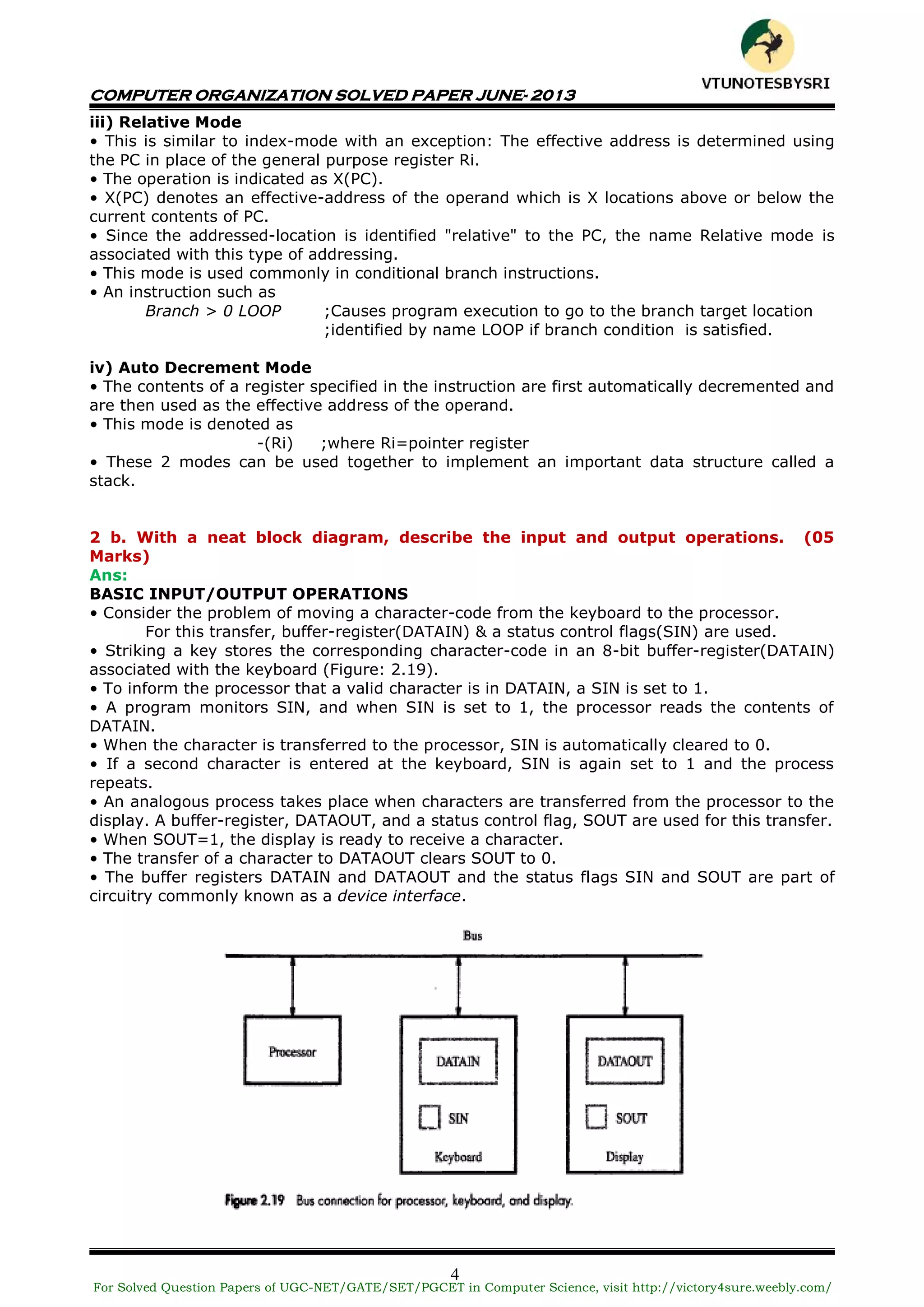
2 a. Define addressing mode. Explain the following addressing modes with an
example for each: (10 Marks)
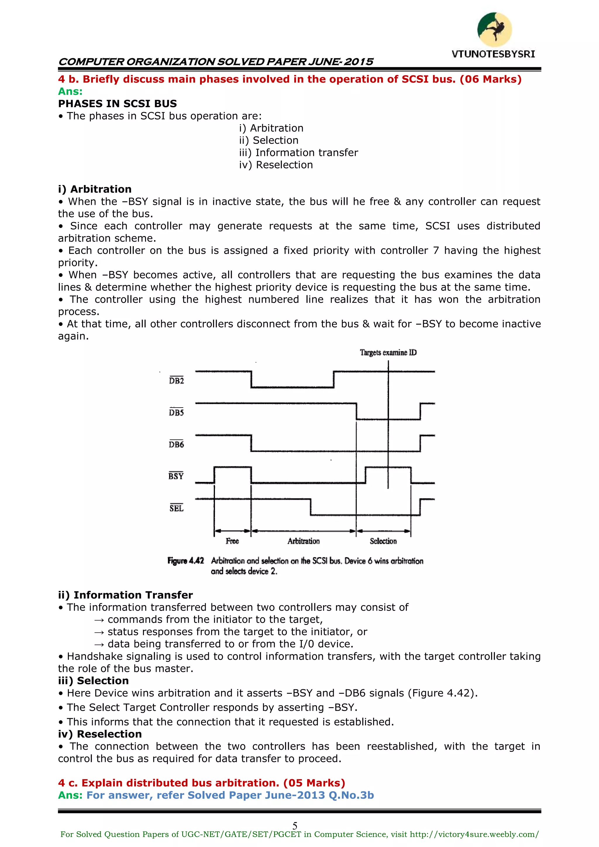
i) index addressing ii) indirect addressing mode
iii) relatve addressing mode iv) auto decrement addressing mode
Ans:
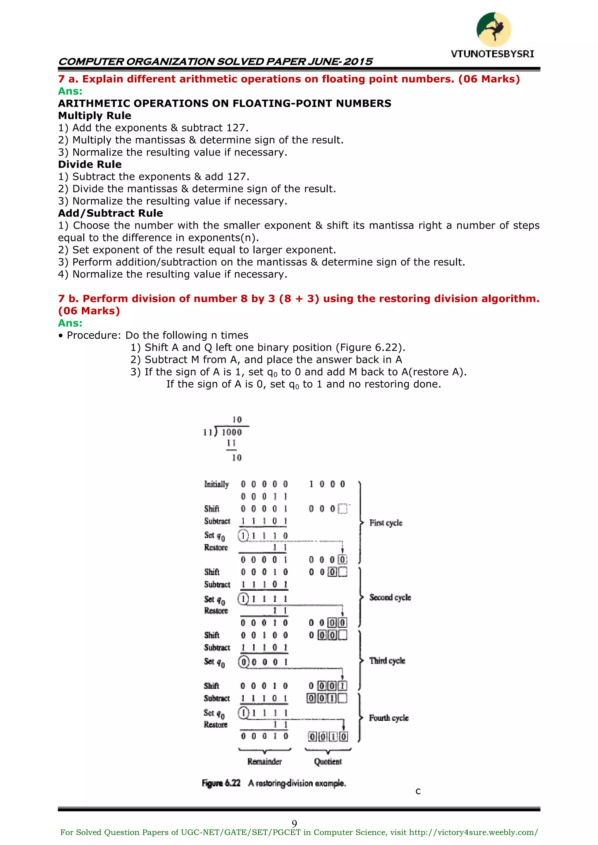
ADDRESSING MODES
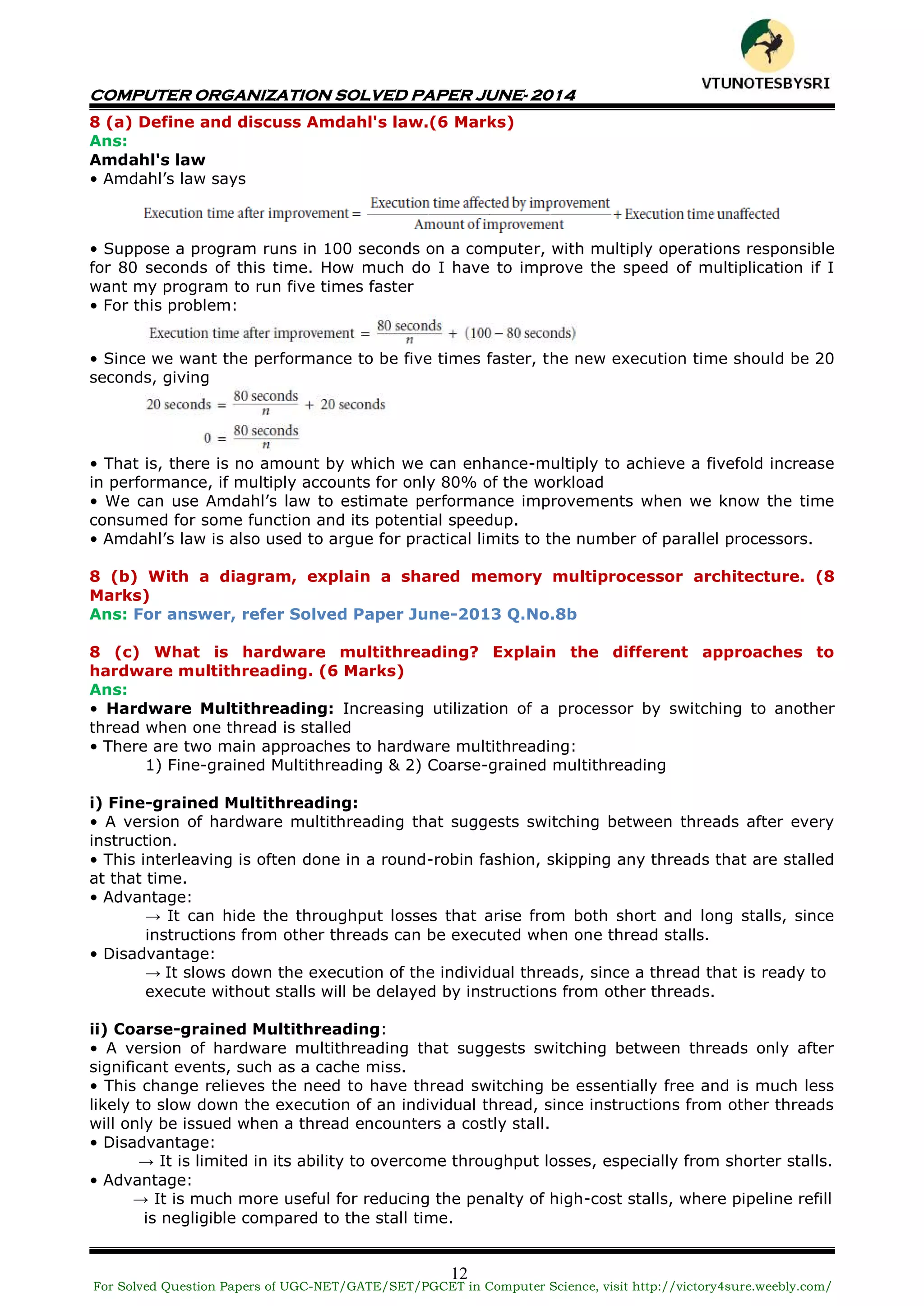
• The different ways in which the location of an operand is specified in an instruction are
referred to as addressing modes (Table 2.1).
i) Index Mode
• The operation is indicated as X(Ri)
where X=the constant value contained in the instruction
Ri=the name of the index register
• The effective-address of the operand is given by EA=X+[Ri]
• The contents of the index-register are not changed in the process of generating the
effective-address (Figure: 2.14).
• In an assembly language program, the constant X may be given either
→ as an explicit number or
→ as a symbolic-name representing a numerical value.
ii) Indirect Mode
• The EA of the operand is the contents of a register(or memory-location) whose address
appears in the instruction.
• The register (or memory-location) that contains the address of an operand is called a
pointer. {The indirection is denoted by ( ) sign around the register or memory-location}.
E.g: Add (R1),R0 ;The operand is in memory. Register R1 gives the effective-
;address(B) of the operand. The data is read from location B and
;added to contents of register R0
For Solved Question Papers of UGC-NET/GATE/SET/PGCET in Computer Science, visit http://victory4sure.weebly.com/
VTU
N
O
TESBYSR
I](https://image.slidesharecdn.com/vtu4thsemcsecomputerorganizationsolvedpapersofjune2013june2014june2015-160604191325/75/VTU-4TH-SEM-CSE-COMPUTER-ORGANIZATION-SOLVED-PAPERS-OF-JUNE-2013-JUNE-2014-JUNE-2015-5-2048.jpg)


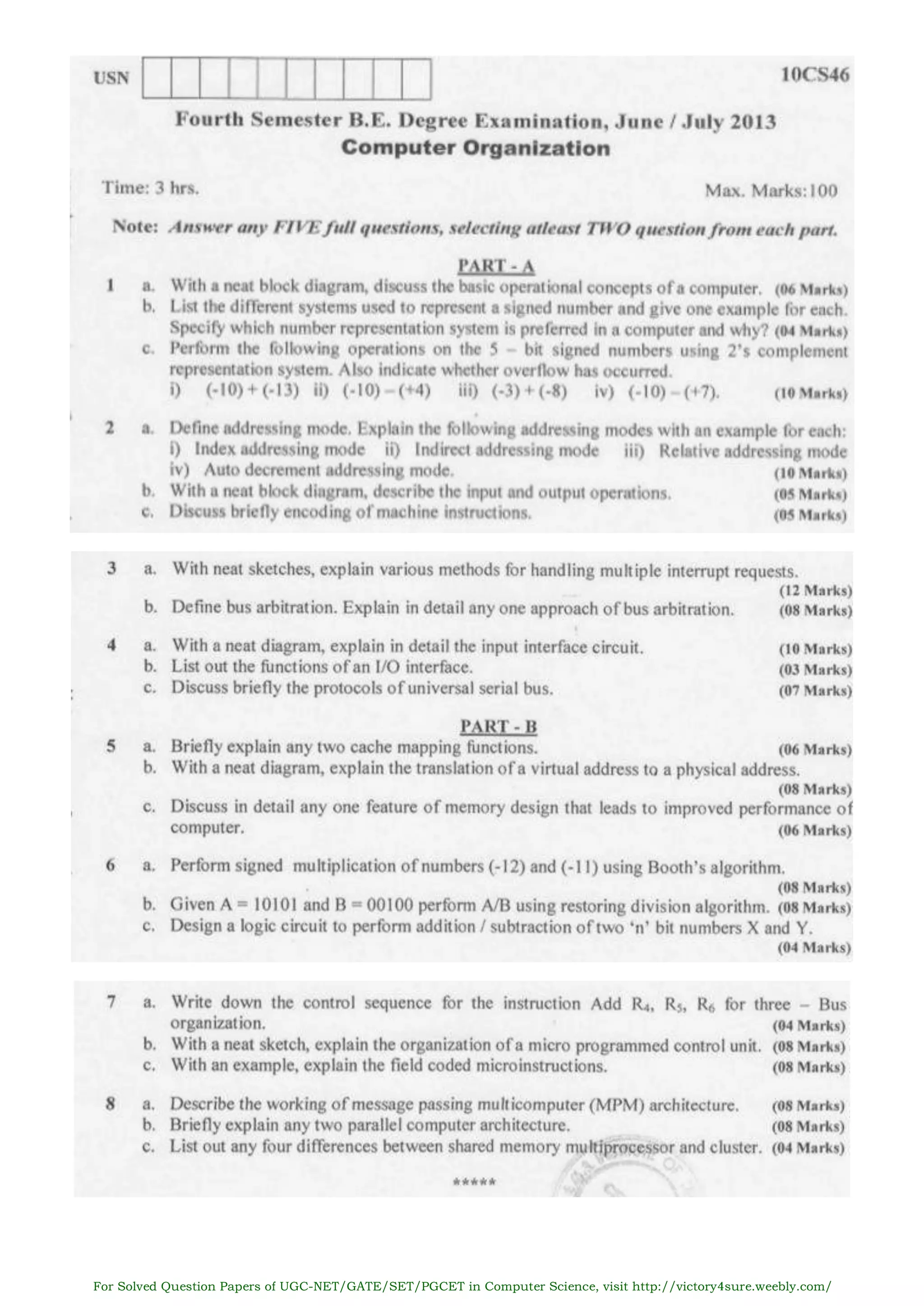
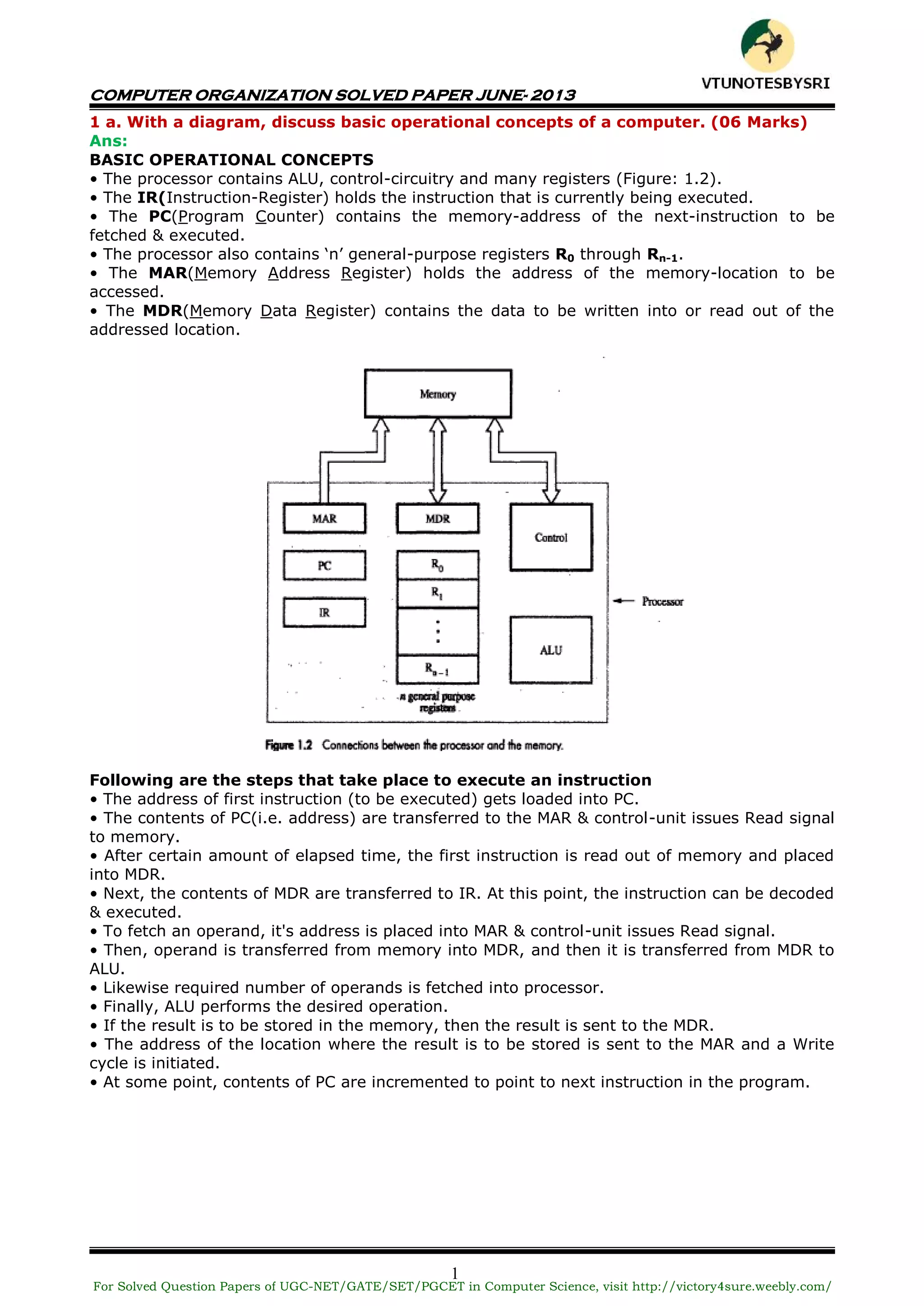
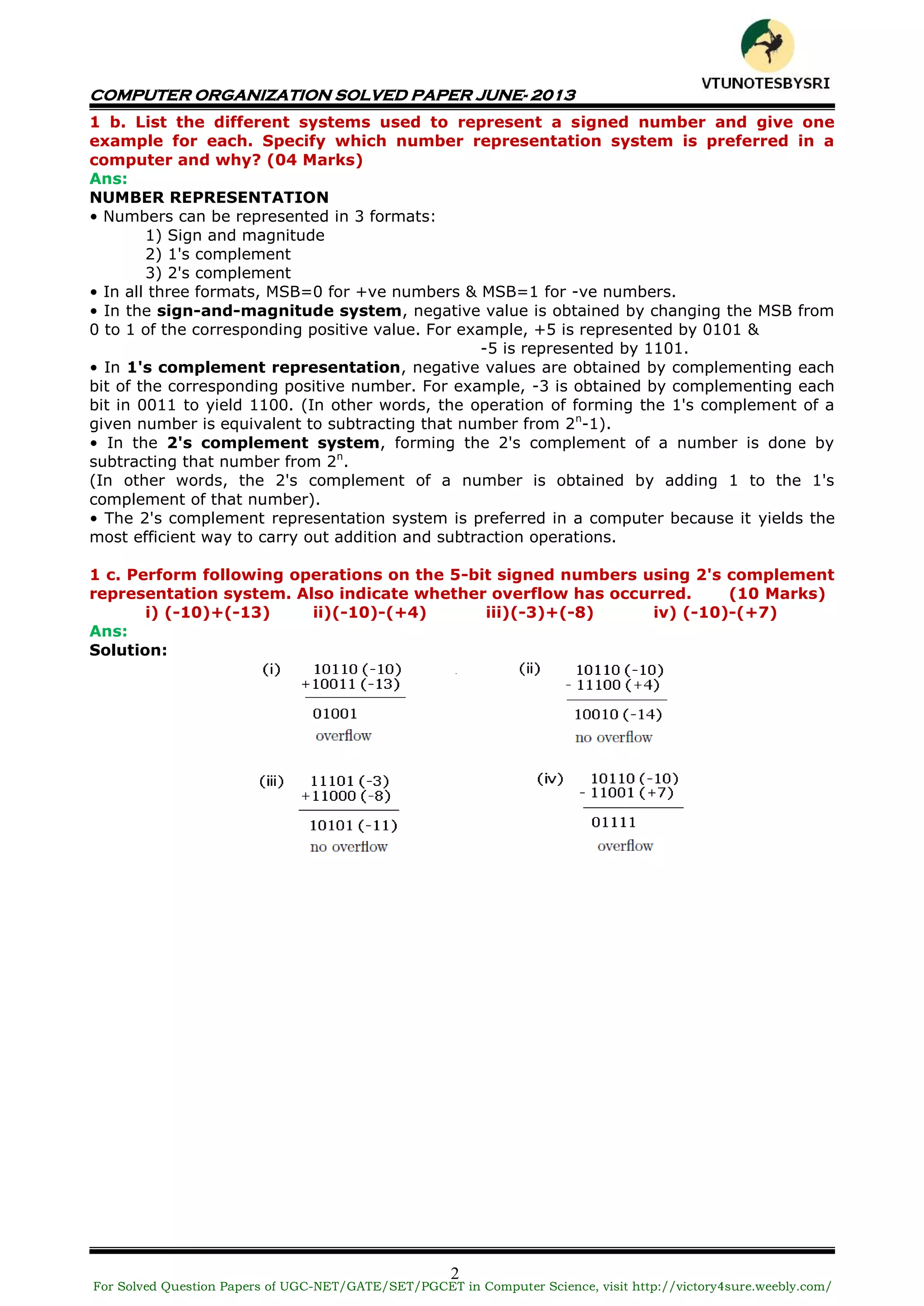
This document contains a solved question paper for Computer Organization from June 2013. It includes questions and detailed answers on topics such as basic computer operations, number representation systems, addressing modes, input/output operations, interrupts, bus arbitration, and the Universal Serial Bus protocol. The solved questions cover concepts, provide examples, and include diagrams to illustrate computer hardware and architecture.