The document discusses timing diagrams and machine cycles in the 8085 microprocessor. It provides details on the different machine cycles - opcode fetch, memory read, memory write, I/O read, and I/O write. It explains that the 8085 has a clock signal divided into T-states that represent portions of machine cycle operations. Examples are given of timing diagrams for instructions like MOV B,C, MVI B,43, and STA 526A to illustrate the sequence of events over multiple T-states.
Changes from one state to another are represented by a change in the level of the lifeline. For the period of time when the object is a given state, the timeline runs parallel to that state. A change in state appears as a vertical change from one level to another. The cause of the change, as is the case in a state or sequence diagram, is the receipt of a message, an event that causes a change, a condition within the system, or even just the passage of time.
The figure below shows an alternative notation of UML Timing diagram. It shows the state of the object between two horizontal lines that cross with each other each time the state changes.
A lifeline in a Timing diagram forms a rectangular space within the content area of a frame. Lifeline is a named element which represents an individual participant in the interaction. It is typically aligned horizontally to read from left to right.
A state or condition timeline represents the set of valid states and time. The states are stacked on the left margin of the lifeline from top to bottom.
We can use the length of a timeline to indicate how long the object remains in a particular state by reading it from left to right. To associate time measurements, you show tick marks online the bottom part of the frame.
The example below shows that the Login event is received three time units after the start of the sequence. To show relative times, you can mark a specific instance in time using a variable name. The figure marks the time the sendMail event is received as time
The word comes from the combination micro and processor.
Processor means a device that processes whatever. In this context processor means a device that processes numbers, specifically binary numbers, 0’s and 1’s.
To process means to manipulate. It is a general term that describes all manipulation. Again in this content, it means to perform certain operations on the numbers that depend on the microprocessor’s design.
all about architecture and memory interfacing. This is the most important lecture for microprocessor.
In computer science you must known about this lecture.
Synthetic Fiber Construction in lab .pptxPavel ( NSTU)
Synthetic fiber production is a fascinating and complex field that blends chemistry, engineering, and environmental science. By understanding these aspects, students can gain a comprehensive view of synthetic fiber production, its impact on society and the environment, and the potential for future innovations. Synthetic fibers play a crucial role in modern society, impacting various aspects of daily life, industry, and the environment. ynthetic fibers are integral to modern life, offering a range of benefits from cost-effectiveness and versatility to innovative applications and performance characteristics. While they pose environmental challenges, ongoing research and development aim to create more sustainable and eco-friendly alternatives. Understanding the importance of synthetic fibers helps in appreciating their role in the economy, industry, and daily life, while also emphasizing the need for sustainable practices and innovation.
Macroeconomics- Movie Location
This will be used as part of your Personal Professional Portfolio once graded.
Objective:
Prepare a presentation or a paper using research, basic comparative analysis, data organization and application of economic information. You will make an informed assessment of an economic climate outside of the United States to accomplish an entertainment industry objective.
Francesca Gottschalk - How can education support child empowerment.pptxEduSkills OECD
Francesca Gottschalk from the OECD’s Centre for Educational Research and Innovation presents at the Ask an Expert Webinar: How can education support child empowerment?
The French Revolution, which began in 1789, was a period of radical social and political upheaval in France. It marked the decline of absolute monarchies, the rise of secular and democratic republics, and the eventual rise of Napoleon Bonaparte. This revolutionary period is crucial in understanding the transition from feudalism to modernity in Europe.
For more information, visit-www.vavaclasses.com
How to Make a Field invisible in Odoo 17Celine George
It is possible to hide or invisible some fields in odoo. Commonly using “invisible” attribute in the field definition to invisible the fields. This slide will show how to make a field invisible in odoo 17.
Acetabularia Information For Class 9 .docxvaibhavrinwa19
Acetabularia acetabulum is a single-celled green alga that in its vegetative state is morphologically differentiated into a basal rhizoid and an axially elongated stalk, which bears whorls of branching hairs. The single diploid nucleus resides in the rhizoid.
Honest Reviews of Tim Han LMA Course Program.pptxtimhan337
Personal development courses are widely available today, with each one promising life-changing outcomes. Tim Han’s Life Mastery Achievers (LMA) Course has drawn a lot of interest. In addition to offering my frank assessment of Success Insider’s LMA Course, this piece examines the course’s effects via a variety of Tim Han LMA course reviews and Success Insider comments.
The Roman Empire A Historical Colossus.pdfkaushalkr1407
The Roman Empire, a vast and enduring power, stands as one of history's most remarkable civilizations, leaving an indelible imprint on the world. It emerged from the Roman Republic, transitioning into an imperial powerhouse under the leadership of Augustus Caesar in 27 BCE. This transformation marked the beginning of an era defined by unprecedented territorial expansion, architectural marvels, and profound cultural influence.
The empire's roots lie in the city of Rome, founded, according to legend, by Romulus in 753 BCE. Over centuries, Rome evolved from a small settlement to a formidable republic, characterized by a complex political system with elected officials and checks on power. However, internal strife, class conflicts, and military ambitions paved the way for the end of the Republic. Julius Caesar’s dictatorship and subsequent assassination in 44 BCE created a power vacuum, leading to a civil war. Octavian, later Augustus, emerged victorious, heralding the Roman Empire’s birth.
Under Augustus, the empire experienced the Pax Romana, a 200-year period of relative peace and stability. Augustus reformed the military, established efficient administrative systems, and initiated grand construction projects. The empire's borders expanded, encompassing territories from Britain to Egypt and from Spain to the Euphrates. Roman legions, renowned for their discipline and engineering prowess, secured and maintained these vast territories, building roads, fortifications, and cities that facilitated control and integration.
The Roman Empire’s society was hierarchical, with a rigid class system. At the top were the patricians, wealthy elites who held significant political power. Below them were the plebeians, free citizens with limited political influence, and the vast numbers of slaves who formed the backbone of the economy. The family unit was central, governed by the paterfamilias, the male head who held absolute authority.
Culturally, the Romans were eclectic, absorbing and adapting elements from the civilizations they encountered, particularly the Greeks. Roman art, literature, and philosophy reflected this synthesis, creating a rich cultural tapestry. Latin, the Roman language, became the lingua franca of the Western world, influencing numerous modern languages.
Roman architecture and engineering achievements were monumental. They perfected the arch, vault, and dome, constructing enduring structures like the Colosseum, Pantheon, and aqueducts. These engineering marvels not only showcased Roman ingenuity but also served practical purposes, from public entertainment to water supply.
Unit 8 - Information and Communication Technology (Paper I).pdfThiyagu K
This slides describes the basic concepts of ICT, basics of Email, Emerging Technology and Digital Initiatives in Education. This presentations aligns with the UGC Paper I syllabus.
Embracing GenAI - A Strategic ImperativePeter Windle
Artificial Intelligence (AI) technologies such as Generative AI, Image Generators and Large Language Models have had a dramatic impact on teaching, learning and assessment over the past 18 months. The most immediate threat AI posed was to Academic Integrity with Higher Education Institutes (HEIs) focusing their efforts on combating the use of GenAI in assessment. Guidelines were developed for staff and students, policies put in place too. Innovative educators have forged paths in the use of Generative AI for teaching, learning and assessments leading to pockets of transformation springing up across HEIs, often with little or no top-down guidance, support or direction.
This Gasta posits a strategic approach to integrating AI into HEIs to prepare staff, students and the curriculum for an evolving world and workplace. We will highlight the advantages of working with these technologies beyond the realm of teaching, learning and assessment by considering prompt engineering skills, industry impact, curriculum changes, and the need for staff upskilling. In contrast, not engaging strategically with Generative AI poses risks, including falling behind peers, missed opportunities and failing to ensure our graduates remain employable. The rapid evolution of AI technologies necessitates a proactive and strategic approach if we are to remain relevant.
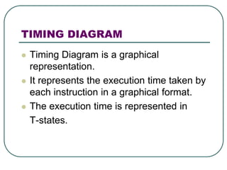
1. TIMING DIAGRAM
Timing Diagram is a graphical
representation.
It represents the execution time taken by
each instruction in a graphical format.
The execution time is represented in
T-states.
4. MACHINE CYCLE
The time required to access the memory
or input/output devices is called machine
cycle.
5. T-STATE
The machine cycle and instruction cycle
takes multiple clock periods.
A portion of an operation carried out in
one system clock period is called as T-
state.
6. MACHINE CYCLES OF 8085
The 8085 microprocessor has 5 basic machine
cycles.
They are
1. Opcode fetch cycle (4T)
2. Memory read cycle (3 T)
3. Memory write cycle (3 T)
4. I/O read cycle (3 T)
5. I/O write cycle (3 T)
7. MACHINE CYCLES OF 8085
The processor takes a definite time to
execute the machine cycles. The time
taken by the processor to execute a
machine cycle is expressed in T-states.
One T-state is equal to the time period of
the internal clock signal of the processor.
The T-state starts at the falling edge of a
clock.
8. OPCODE FETCH MACHINE
CYCLE OF 8085
Each instruction of the processor has one byte opcode.
The opcodes are stored in memory. So, the processor
executes the opcode fetch machine cycle to fetch the
opcode from memory.
Hence, every instruction starts with opcode fetch machine
cycle.
The time taken by the processor to execute the opcode
fetch cycle is 4T.
In this time, the first, 3 T-states are used for fetching the
opcode from memory and the remaining T-states are
used for internal operations by the processor.
10. MEMORY READ MACHINE
CYCLE OF 8085
The memory read machine cycle is executed
by the processor to read a data byte from
memory.
The processor takes 3T states to execute this
cycle
The instructions which have more than one
byte word size will use the machine cycle after
the opcode fetch machine cycle.
12. MEMORY WRITE MACHINE
CYCLE OF 8085
The memory write machine cycle is
executed by the processor to write a
data byte in a memory location.
The processor takes, 3T states to
execute this machine cycle
14. I/O READ CYCLE OF 8085
The I/O Read cycle is executed by the
processor to read a data byte from I/O
port or from the peripheral.
The processor takes 3T states to
execute this machine cycle.
The IN instruction uses this machine
cycle during the execution.
17. I/O WRITE CYCLE OF 8085
The I/O write machine cycle is executed
by the processor to write a data byte in
the I/O port or to a peripheral, which is
I/O, mapped in the system.
The processor takes, 3T states to
execute this machine cycle.
18. Timing diagram
Problem – Draw the timing diagram of
the given instruction in 8085
MOV B, C
Given instruction copy the contents of
the source register into the destination
register and the contents of the source
register are not altered.
19. Timing diagram
MOV B, C
Opcode: MOV
Operand: B and C
Here the destination register and C is the
source register whose contents need to be
transferred to the destination register.
Algorithm – The instruction MOV B, C is of 1
byte; therefore the complete instruction will
be stored in a single memory address
20. Timing diagram
2000: MOV B, C
Only opcode fetching is required for this
instruction and thus we need 4 T states
for the timing diagram. For the opcode
fetch the IO/M (low active) = 0, S1 = 1
and S0 = 1
22. Explanation of diagram
00 – lower bit of address where the opcode is stored, i.e., 00.
20 – higher bit of address where the opcode is stored, i.e., 20.
ALE – provides signal for multiplexed address and data bus. Only in t1
is it used as an address bus to fetch a lower bit of address otherwise it
will be used as the data bus.
RD (low active) – signal is 1 in t1 & t4 as no data is read by the
microprocessor. Signal is 0 in t2 & t3 because here the data is read by
a microprocessor.
WR (low active) – signal is 1 throughout, no data is written by a
microprocessor.
IO/M (low active) – signal is 1 throughout because the operation is
performing on memory.
S0 and S1 – both are 1 in case of opcode fetching.
23. Draw the timing diagram of the following
code,
MVI B, 43
24. Explanation of the command
It stores the immediate 8 bit data to a
register or memory location.
Example: MVI B, 43
Opcode: MVI
Operand: B is the destination register and 43
is the source data which needs to be
transferred to the register.
’43’ data will be stored in the B register.
25. Explanation of the command
Assume the memory address of the opcode and the data. For
example:
MVI B, 43
2000: Opcode
2001: 43
The opcode fetch will be same in all the instructions.
Only the read instruction of the opcode needs to be added in
the successive T states.
For the opcode fetch the IO/M (low active) = 0, S1 = 1 and S0 =
1. Also, 4 T states will be required to fetch the opcode from
memory.
For the opcode read the IO/M (low active) = 0, S1 = 1 and S0 =
0. Also, only 3 T states will be required to read data from
memory.
27. In Opcode fetch ( t1-t4 T states )
00 – lower bit of address where opcode is stored.
20 – higher bit of address where opcode is stored.
ALE – Provides signal for multiplexed address and data bus. Only in t1
it used as address bus to fetch lower bit of address otherwise it will be
used as data bus.
RD (low active) – Signal is 1 in t1 & t4, no data is read by
microprocessor. Signal is 0 in t2 & t3, data is read by microprocessor.
WR (low active) – Signal is 1 throughout, no data is written by
microprocessor.
IO/M (low active) – Signal is 0 in throughout, operation is performing
on memory.
S0 and S1 – Signal is 1 in t1 to t4 states, as to fetch the opcode from
the memory.
28. In Opcode read ( t5-t7 T states )
01 – lower bit of address where data is stored.
20 – higher bit of address where data is stored.
ALE – Provides signal for multiplexed address and data bus. Only in t5 it used
as address bus to fetch lower bit of address otherwise it will be used as data
bus.
RD (low active) – Signal is 1 in t5 as no data is read by microprocessor. Signal
is 0 in t6 & t7 as data is read by microprocessor.
WR (low active) – Signal is 1 throughout, no data is written by microprocessor.
IO/M (low active) – Signal is 0 in throughout, operation is performing on
memory.
S0 – Signal is 0 in throughout, operation is performing on memory to read data
43.
S1 – Signal is 1 throughout, operation is performing on memory to read data
43.
30. Timing Diagram for STA 526AH
STA means Store Accumulator -The content of the accumulator is
stored in the specified address (526A). this instruction SDA 4050H
requires 3-Bytes, 4-Machine Cycles (Opcode Fetch, Memory Read,
Memory Read, Memory Write) and 13 T-States for execution
The op-code of the STA instruction is said to be 32H. It is fetched from
the memory 41FFH (see fig). - OF machine cycle
Then the lower order memory address is read (6A). – Memory Read
Machine Cycle
Read the higher order memory address (52).- Memory Read Machine
Cycle
The combination of both the addresses is considered and the content
from accumulator is written in 526A. – Memory Write Machine Cycle
Assume the memory address for the instruction and let the content of
accumulator is C7H. So, C7H from accumulator is now stored in 526A
31. Explanation of the command
Address Memories Hex-code
41FFH STA 32H
4200H 6AH 6AH
4201H 52H 52H
526AH C7H C7H
33. OUT a8 instruction in 8085
Microprocessor
OUT is a mnemonic that stands for
OUTput Accumulator contents to an
output port whose8-bit address is
indicated in the instruction . It occupies 2
Bytes in the memory. First Byte specifies
the opcode, and the next Byte provides
the 8-bit port address.
34. Explanation of the command
Mnemonics, Operand Opcode(in HEX) Bytes
OUT Port-Address D3 2
35. Explanation of the command
OUT instruction is the only instruction using
which Accumulator contents can be sent out
to an output port. A possible chip select
circuit to connect an output port with an
address as F0H.
So this instruction OUT requires 2-Bytes, 3-
Machine Cycles (Opcode Fetch, Memory
Read, I/O write) and 10 T-States
36. Explanation of the command
Addr
ess
Hex
Code
s
Mnemo
nic
Comment
200
0
D3 OUT
F0H
Accumulator content will be sent to
port addressF0H
201 F0 F0H as port address