Downloaded 392 times
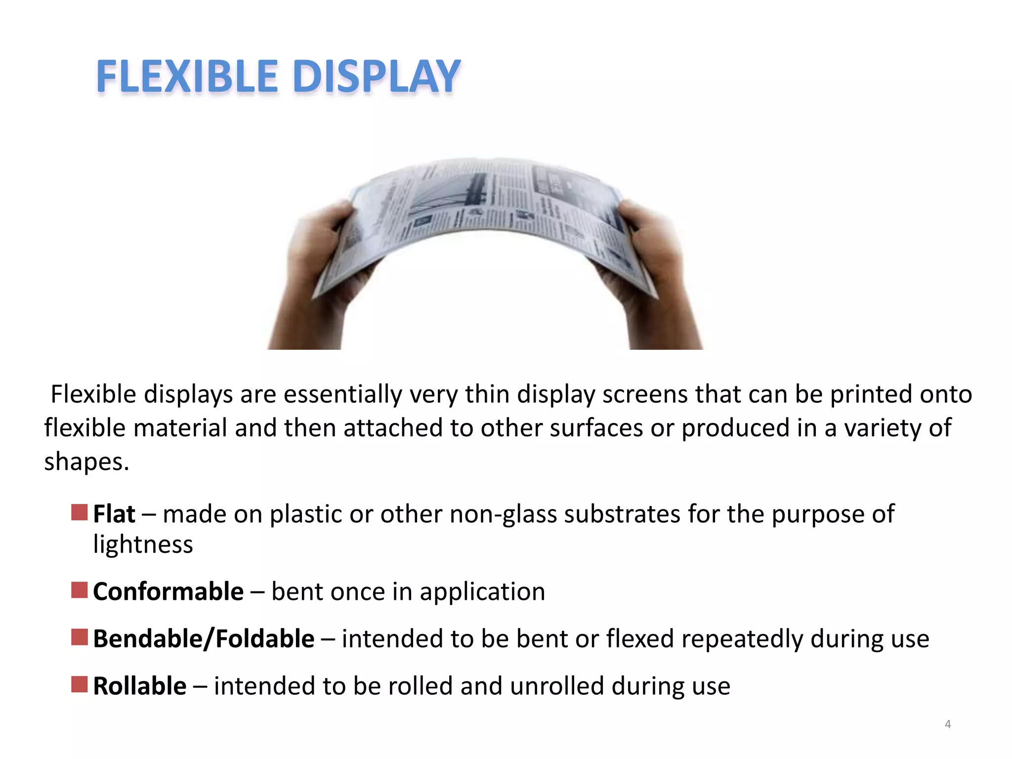

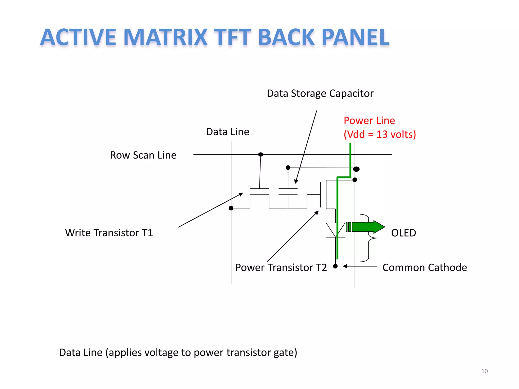
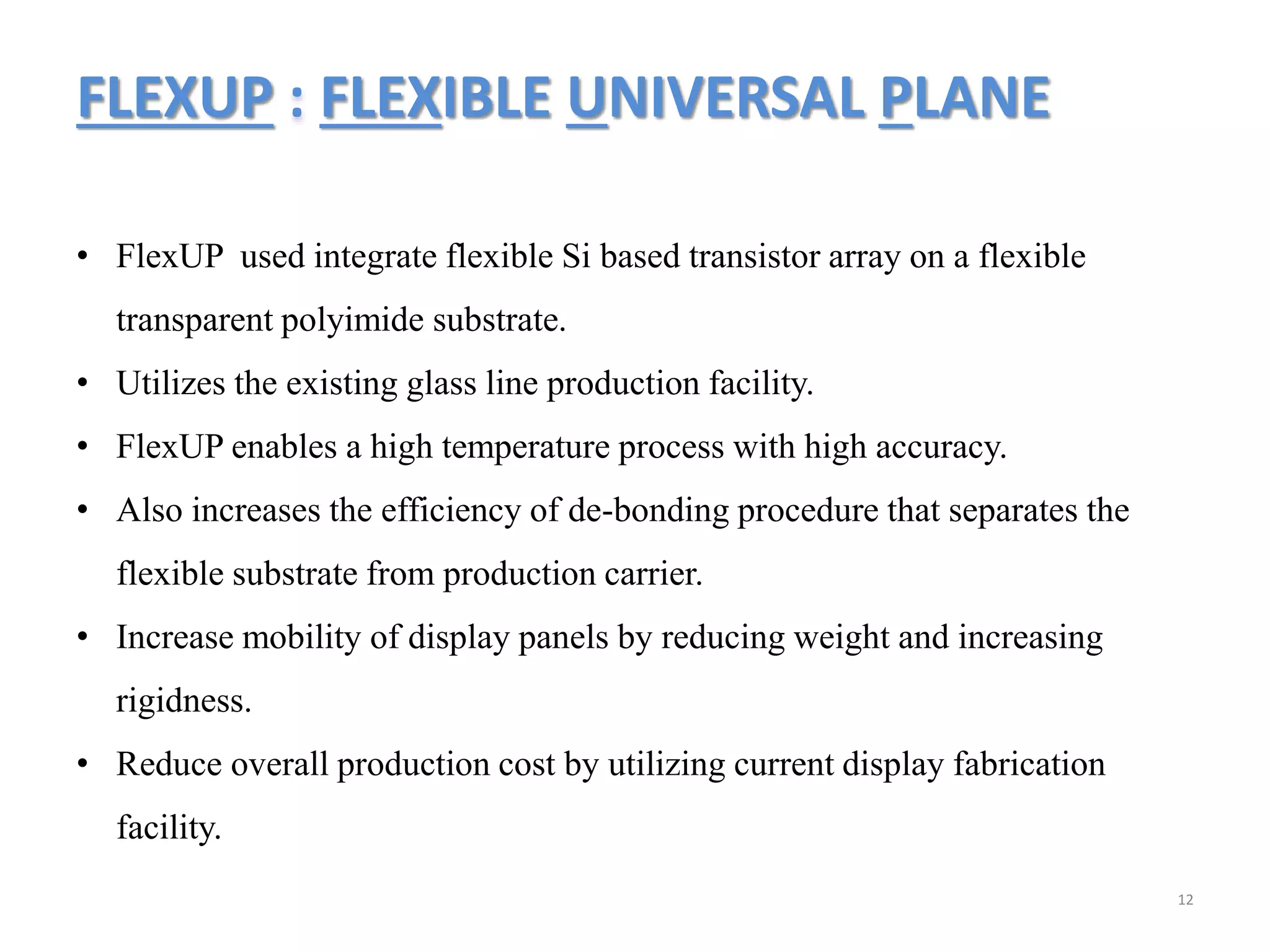
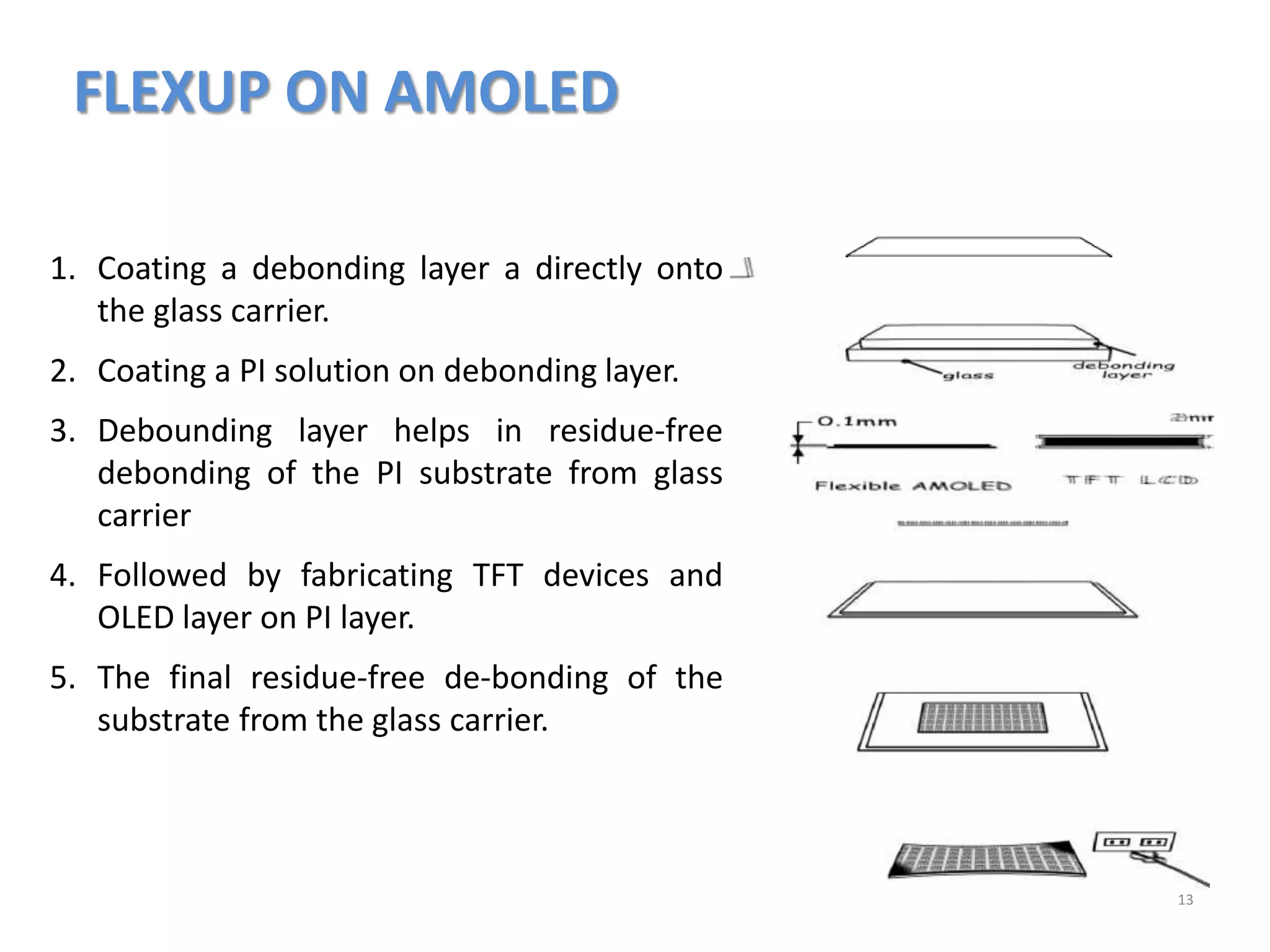
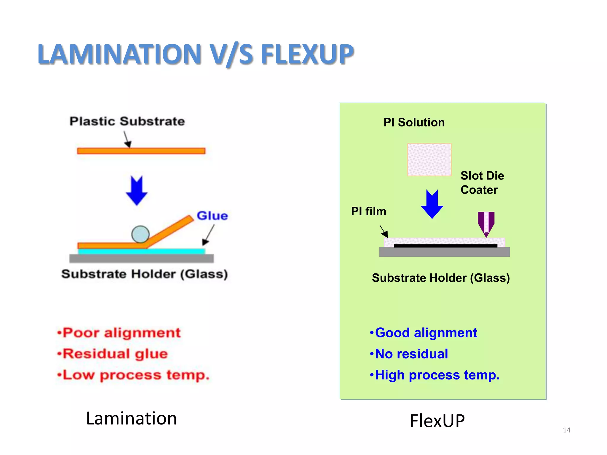
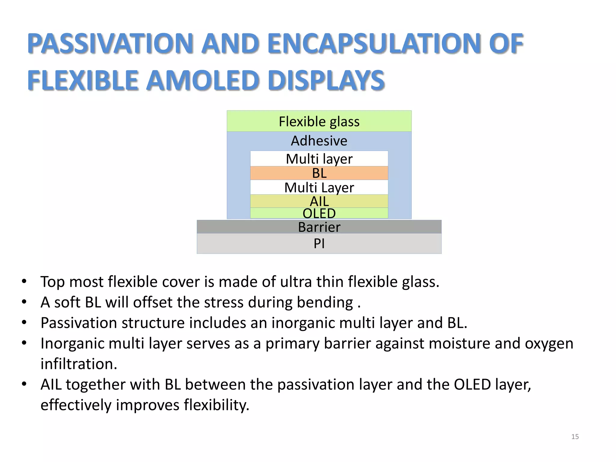
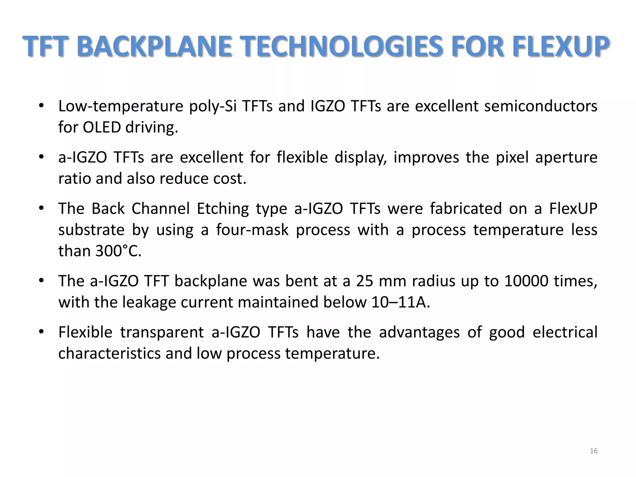
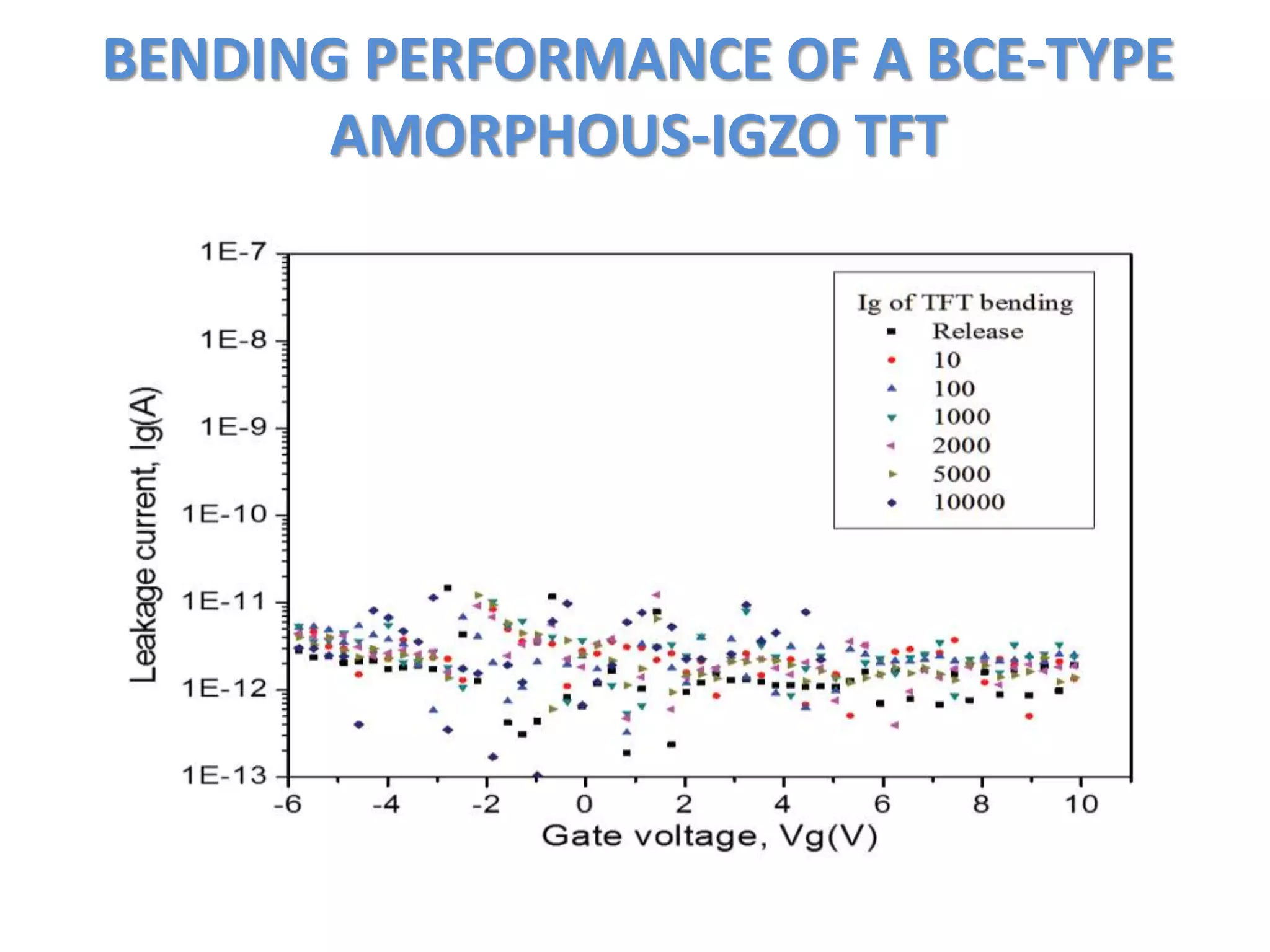
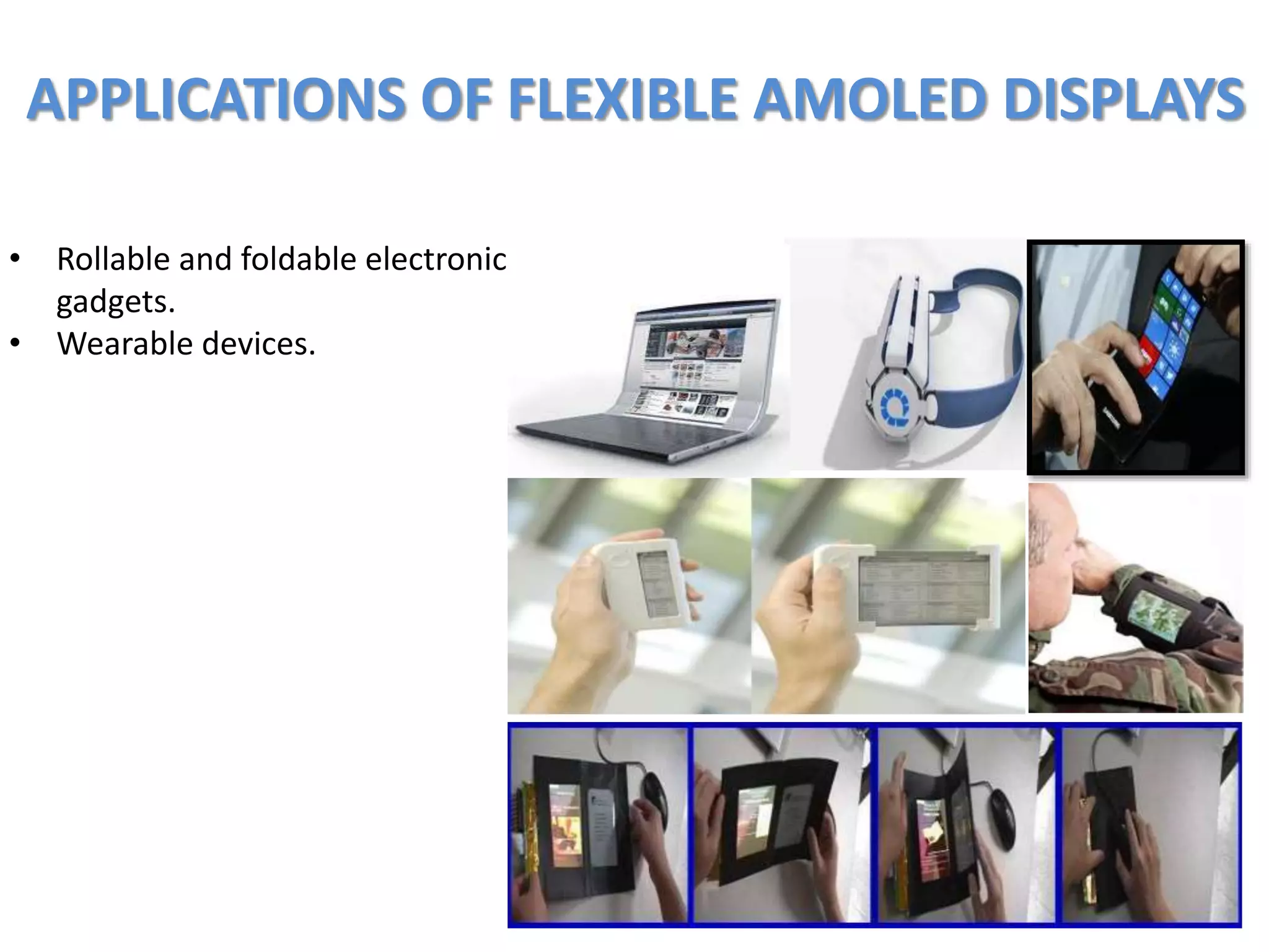
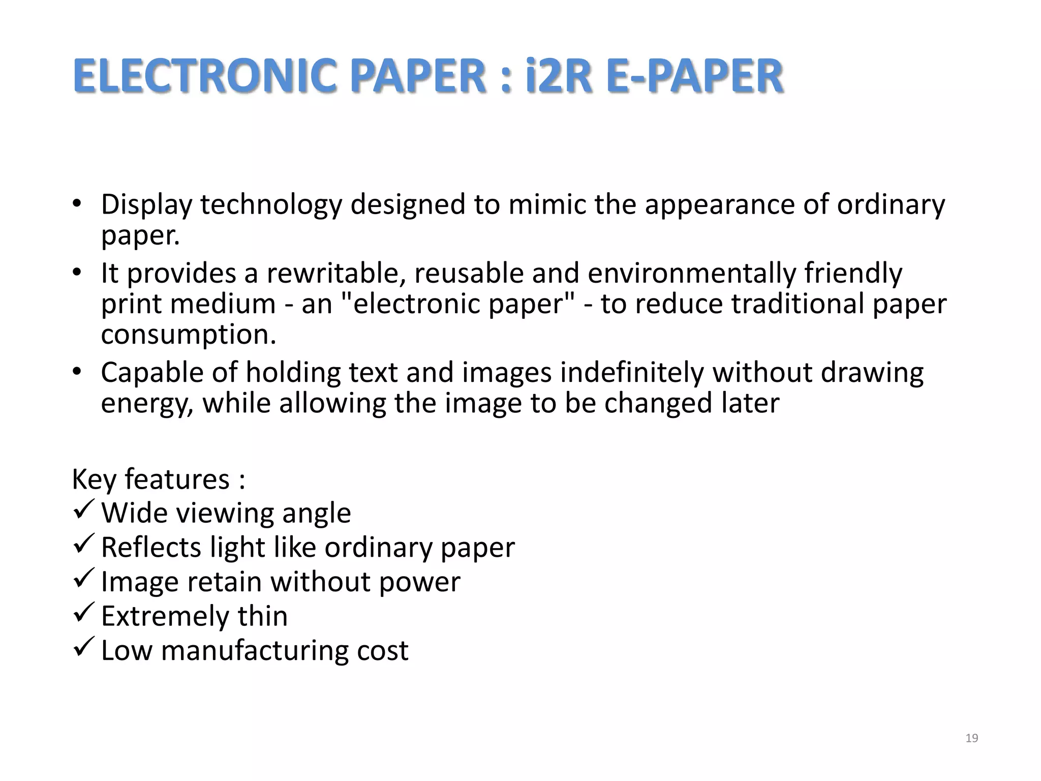

Flexible displays can be produced on plastic or other flexible materials and attached to surfaces in various shapes. AMOLED displays are well-suited for flexible displays as they do not require backlighting and can be produced using roll-to-roll manufacturing. The FlexUp technology allows for high temperature processing of flexible displays on glass carriers before debonding and transferring the circuitry onto flexible plastic substrates. Passivation layers and encapsulation techniques help protect flexible AMOLEDs from stress and moisture during bending. i2R e-paper uses liquid crystals and pigment layers that reflect light to display images without power by mimicking the appearance of ordinary paper.


![AMOLED [Active Matrix Organic LED] by NITIN GUPTA](https://cdn.slidesharecdn.com/ss_thumbnails/amoledfinal-180222150218-thumbnail.jpg?width=640&height=640&fit=bounds)


