Download to read offline


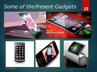
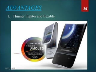
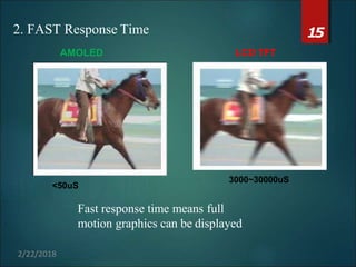
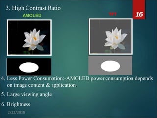


The document provides an overview of Active Matrix Organic Light Emitting Diode (AMOLED) technology, detailing its components, working principles, manufacturing processes, and comparisons to other display technologies. It discusses applications such as mobile phones, TVs, and tablets, along with advantages like flexibility and lower power consumption, and disadvantages like limited lifetime and complex manufacturing. Future prospects include advancements like curved and transparent AMOLED displays, indicating the potential for widespread replacement of current LED and LCD technologies.


![[ amoled display]](https://cdn.slidesharecdn.com/ss_thumbnails/rakeshamoleddisplay-160912144947-thumbnail.jpg?width=640&height=640&fit=bounds)


