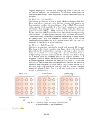
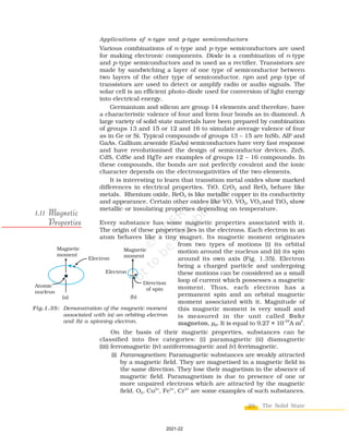
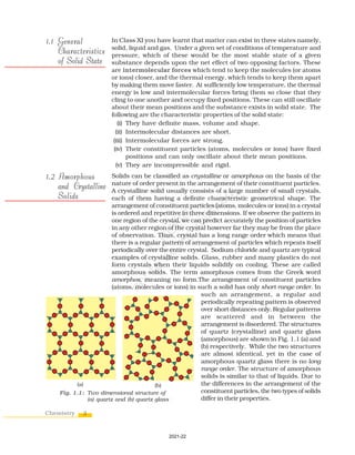
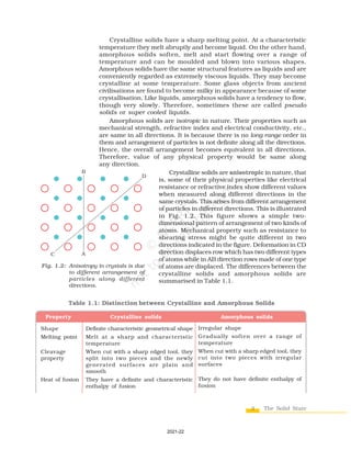
The document discusses different types of solids and their properties. Crystalline solids have long-range ordered structures that repeat periodically, while amorphous solids only have short-range order. Crystalline solids can be anisotropic with properties varying in different directions, whereas amorphous solids are isotropic with uniform properties in all directions. Common examples of crystalline solids are sodium chloride and quartz, while glass and rubber are typically amorphous. The vast majority of solid substances are either crystalline or polycrystalline rather than purely amorphous. Crystalline solids can be further classified based on the type of bonding forces between their constituent particles as molecular, ionic, metallic, or covalent


![18
Chemistry
those of the first layer as shown in Figs. 1.22 and 1.23. This pattern
of layers is often written as ABCABC ........... This structure is called
cubic close packed (ccp) or face-centred cubic (fcc) structure. Metals
such as copper and silver crystallise in this structure.
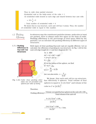
Both these types of close packing are highly efficient and 74%
space in the crystal is filled. In either of them, each sphere is in contact
with twelve spheres. Thus, the coordination number is 12 in either of
these two structures.
Earlier in the section, we have learnt that when particles are close-
packed resulting in either ccp or hcp structure, two types of voids are
generated. While the number of octahedral voids present in a lattice is
equal to the number of close packed particles, the number of tetrahedral
voids generated is twice this number. In ionic solids, the bigger ions
(usually anions) form the close packed structure and the smaller ions
(usually cations) occupy the voids. If the latter ion is small enough
then tetrahedral voids are occupied, if bigger, then octahedral voids. All
octahedral or tetrahedral voids are not occupied. In a given compound,
the fraction of octahedral or tetrahedral voids that are occupied, depends
upon the chemical formula of the compound, as can be seen from the
following examples.
We know that close packed structures have both tetrahedral and octahedral
voids. Let us take ccp (or fcc) structure and locate these voids in it.
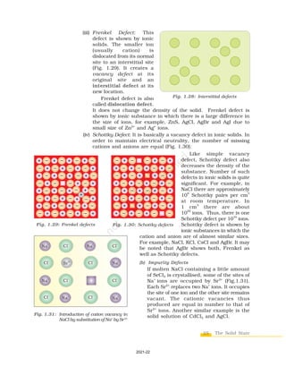
(a) Locating Tetrahedral Voids
Let us consider a unit cell of ccp or fcc lattice [Fig. 1(a)]. The unit cell is divided
into eight small cubes.
Example 1.1
Example 1.1
Example 1.1
Example 1.1
Example 1.1
1.6.1 Formula of a
Compound
and Number
of Voids
Filled
A compound is formed by two elements X and Y. Atoms of the element
Y (as anions) make ccp and those of the element X (as cations) occupy
all the octahedral voids. What is the formula of the compound?
The ccp lattice is formed by the element Y. The number of octahedral
voids generated would be equal to the number of atoms of Y present in
it. Since all the octahedral voids are occupied by the atoms of X, their
number would also be equal to that of the element Y. Thus, the atoms
of elements X and Y are present in equal numbers or 1:1 ratio. Therefore,
the formula of the compound is XY.
Atoms of element B form hcp lattice and those of the element A occupy
2/3rd of tetrahedral voids. What is the formula of the compound formed
by the elements A and B?
The number of tetrahedral voids formed is equal to twice the number of
atoms of element B and only 2/3rd of these are occupied by the atoms
of element A. Hence the ratio of the number of atoms of A and B is 2
× (2/3):1 or 4:3 and the formula of the compound is A4
B3
.
Example 1.2
Example 1.2
Example 1.2
Example 1.2
Example 1.2
Solution
Solution
Solution
Solution
Solution
Solution
Solution
Solution
Solution
Solution
Locating Tetrahedral and Octahedral Voids
Locating Tetrahedral and Octahedral Voids
Locating Tetrahedral and Octahedral Voids
Locating Tetrahedral and Octahedral Voids
Locating Tetrahedral and Octahedral Voids
2021-22](https://image.slidesharecdn.com/solidstate-240228132046-07209622/85/solid-state-ncert-class-11-text-book-pdf-18-320.jpg)
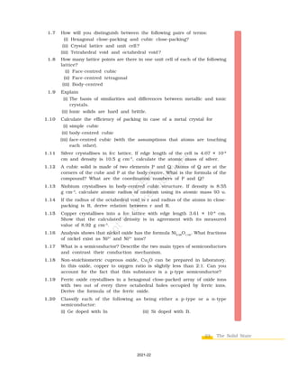
![19 The Solid State
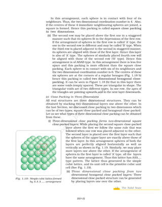
Each small cube has atoms at alternate corners [Fig. 1(a)]. In all, each small
cube has 4 atoms. When joined to each other, they make a regular tetrahedron.
Thus, there is one tetrahedral void in each small cube and eight tetrahedral
voids in total. Each of the eight small cubes have one void in one unit cell of ccp
structure. We know that ccp structure has 4 atoms per unit cell. Thus, the
number of tetrahedral voids is twice the number of atoms.
Fig. 1: (a) Eight tetrahedral voids per unit cell of ccp structure
(b) one tetrahedral void showing the geometry.
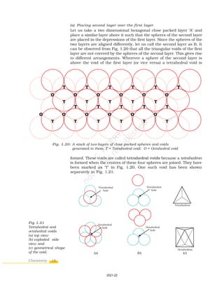
(b) Locating Octahedral Voids
Let us again consider a unit cell of ccp or fcc lattice [Fig. 2(a)]. The body centre
of the cube, C is not occupied but it is surrounded by six atoms on face centres.
If these face centres are joined, an octahedron is generated. Thus, this unit cell
has one octahedral void at the body centre of the cube.
Besides the body centre, there is one octahedral void at the centre of each
of the 12 edges [Fig. 2(b)]. It is surrounded by six atoms, four belonging to the
same unit cell (2 on the corners and 2 on face centre) and two belonging to two
adjacent unit cells. Since each edge of the cube is shared between four adjacent
unit cells, so is the octahedral void located on it. Only
1
4
th
of each void belongs
to a particular unit cell.
(a) (b)
Fig. 2: Location of octahedral voids per unit cell of ccp or fcc lattice (a) at the body centre
of the cube and (b) at the centre of each edge (only one such void is shown).
2021-22](https://image.slidesharecdn.com/solidstate-240228132046-07209622/85/solid-state-ncert-class-11-text-book-pdf-19-320.jpg)