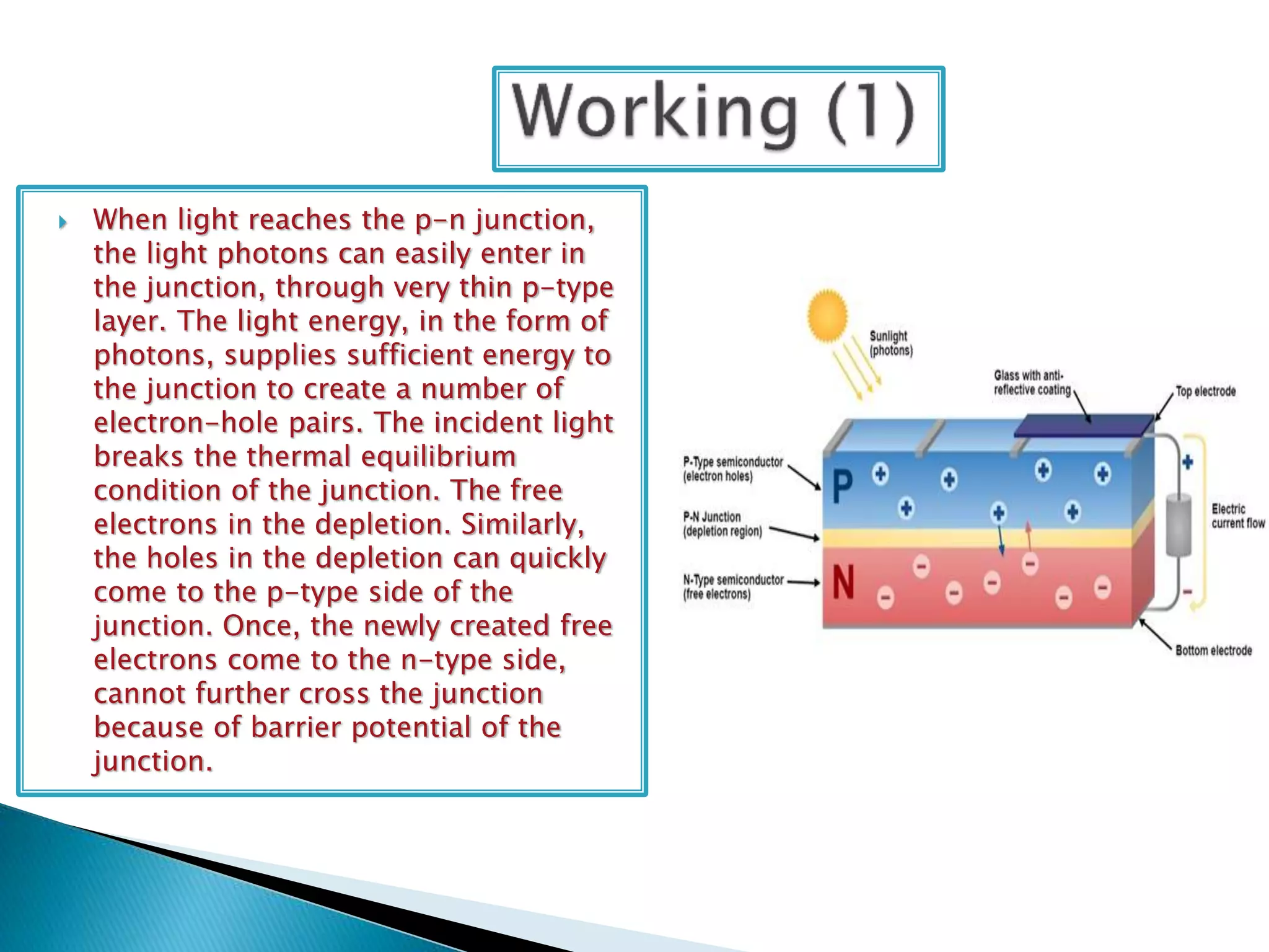
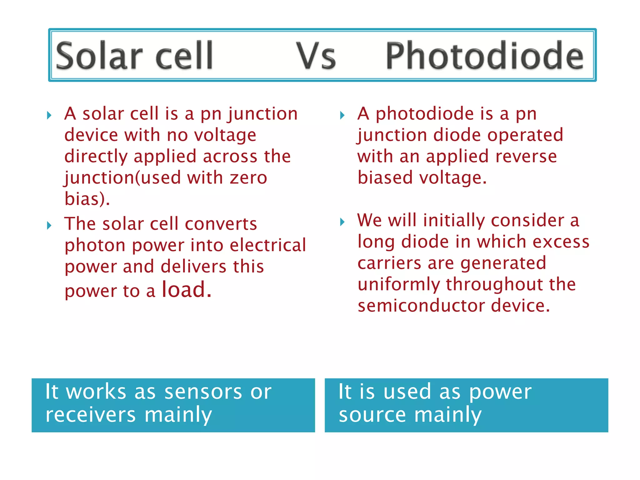
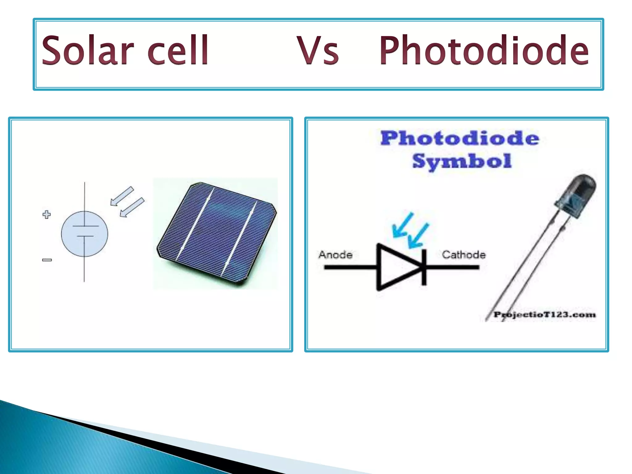
Submitted to Submitted by
A solar cell, or photovoltaic
cell, is an electrical device
that converts the energy of light
directly into electricity
by the photovoltaic effect
which is a physical
and chemical phenomenon.
 The solar cells are based on
the principle of photovoltaic
effect.
 The generation of voltage
across the p-n junction in a
semiconductor due to the
absorption of light radiaton is
called photovoltaic effect.
 When light reaches the p-n junction,
the light photons can easily enter in
the junction, through very thin p-type
layer. The light energy, in the form of
photons, supplies sufficient energy to
the junction to create a number of
electron-hole pairs. The incident light
breaks the thermal equilibrium
condition of the junction. The free
electrons in the depletion. Similarly,
the holes in the depletion can quickly
come to the p-type side of the
junction. Once, the newly created free
electrons come to the n-type side,
cannot further cross the junction
because of barrier potential of the
junction.
Similarly, the newly created holes once
come to the p-type side cannot further
cross the junction became of same barrier
potential of the junction. As the
concentration of electrons becomes higher
in one side, i.e. n-type side of the junction
and concentration of holes becomes more
in another side, i.e. the p-type side of the
junction, the p-n junction will behave like a
small battery cell. A voltage is set up which
is known as photo voltage. If we connect a
small load across the junction, there will be
a tiny current flowing through it, n region
can quickly come to the n-type side of the
junction.
Solar panel type Advantages Disadvantages
Monocrystalline
•High
efficiency/perform
ance
•Aesthetics
•Higher costs
Polycrystalline •Low cost
•Lower
efficiency/perform
ance
Thin-film
•Portable and
flexible
•Lightweight
•Aesthetics
•Lowest
efficiency/perform
ance
The materials which are
used for this purpose
must have band gap close
to 1.5ev. Commonly used
materials are-
 Silicon.
 GaAs.
 CdTe.
 CuInSe2
It works as sensors or
receivers mainly
It is used as power
source mainly
 A solar cell is a pn junction
device with no voltage
directly applied across the
junction(used with zero
bias).
 The solar cell converts
photon power into electrical
power and delivers this
power to a load.
 A photodiode is a pn
junction diode operated
with an applied reverse
biased voltage.
 We will initially consider a
long diode in which excess
carriers are generated
uniformly throughout the
semiconductor device.
Solar cell
Solar cell

Solar cell

  • 1.
  • 2.
    A solar cell,or photovoltaic cell, is an electrical device that converts the energy of light directly into electricity by the photovoltaic effect which is a physical and chemical phenomenon.
  • 3.
     The solarcells are based on the principle of photovoltaic effect.  The generation of voltage across the p-n junction in a semiconductor due to the absorption of light radiaton is called photovoltaic effect.
  • 4.
     When lightreaches the p-n junction, the light photons can easily enter in the junction, through very thin p-type layer. The light energy, in the form of photons, supplies sufficient energy to the junction to create a number of electron-hole pairs. The incident light breaks the thermal equilibrium condition of the junction. The free electrons in the depletion. Similarly, the holes in the depletion can quickly come to the p-type side of the junction. Once, the newly created free electrons come to the n-type side, cannot further cross the junction because of barrier potential of the junction.
  • 5.
    Similarly, the newlycreated holes once come to the p-type side cannot further cross the junction became of same barrier potential of the junction. As the concentration of electrons becomes higher in one side, i.e. n-type side of the junction and concentration of holes becomes more in another side, i.e. the p-type side of the junction, the p-n junction will behave like a small battery cell. A voltage is set up which is known as photo voltage. If we connect a small load across the junction, there will be a tiny current flowing through it, n region can quickly come to the n-type side of the junction.
  • 7.
    Solar panel typeAdvantages Disadvantages Monocrystalline •High efficiency/perform ance •Aesthetics •Higher costs Polycrystalline •Low cost •Lower efficiency/perform ance Thin-film •Portable and flexible •Lightweight •Aesthetics •Lowest efficiency/perform ance
  • 9.
    The materials whichare used for this purpose must have band gap close to 1.5ev. Commonly used materials are-  Silicon.  GaAs.  CdTe.  CuInSe2
  • 11.
    It works assensors or receivers mainly It is used as power source mainly  A solar cell is a pn junction device with no voltage directly applied across the junction(used with zero bias).  The solar cell converts photon power into electrical power and delivers this power to a load.  A photodiode is a pn junction diode operated with an applied reverse biased voltage.  We will initially consider a long diode in which excess carriers are generated uniformly throughout the semiconductor device.